

Motorola MC74ACT352D, MC74ACT352N, MC74AC352N, MC74AC352D Datasheet
5-1
FACT DATA
The MC74AC352/74ACT352 is a very high-speed dual 4-input multiplexer with
common Select inputs and individual Enable inputs for each section. It can select
two bits of data from four sources. The two buffered outputs present data in the
inverted (complementary) form. The MC74AC352/74ACT352 is the functional
equivalent of the MC74AC153/74ACT153 except with inverted outputs.
• Inverted Version of the MC74AC153/74ACT153
• Separate Enables for Each Multiplexer
• Outputs Source/Sink 24 mA
• ′ACT352 Has TTL Compatible Inputs
1516 14 13 12 11 10
21 3 4 5 6 7
V
CC
9
8
E
bS0I3bI2bI1bI0bZb
E
aS1I3aI2aI1aI0aZa
GND
PIN NAMES
I0a–I
3a
Side A Data Inputs
I0b–I
3b
Side B Data Inputs
S0, S1Common Select Inputs
E
a
Side A Enable Input
E
b
Side B Enable Input
Z
a, Zb
Multiplexer Outputs
TRUTH TABLE
Select Inputs Inputs (a or b) Output
S
0
S
1
E I0 I1I2I
3
Z
X X H X X X X H
L L L L X X X H
L L L H X X X L
H L L X L X X H
H L L X H X X L
L H L X X L X H
L H L X X H X L
H H L X X X L H
H H L X X X H L
H = HIGH Voltage Level
L = LOW Voltage Level
X = Immaterial
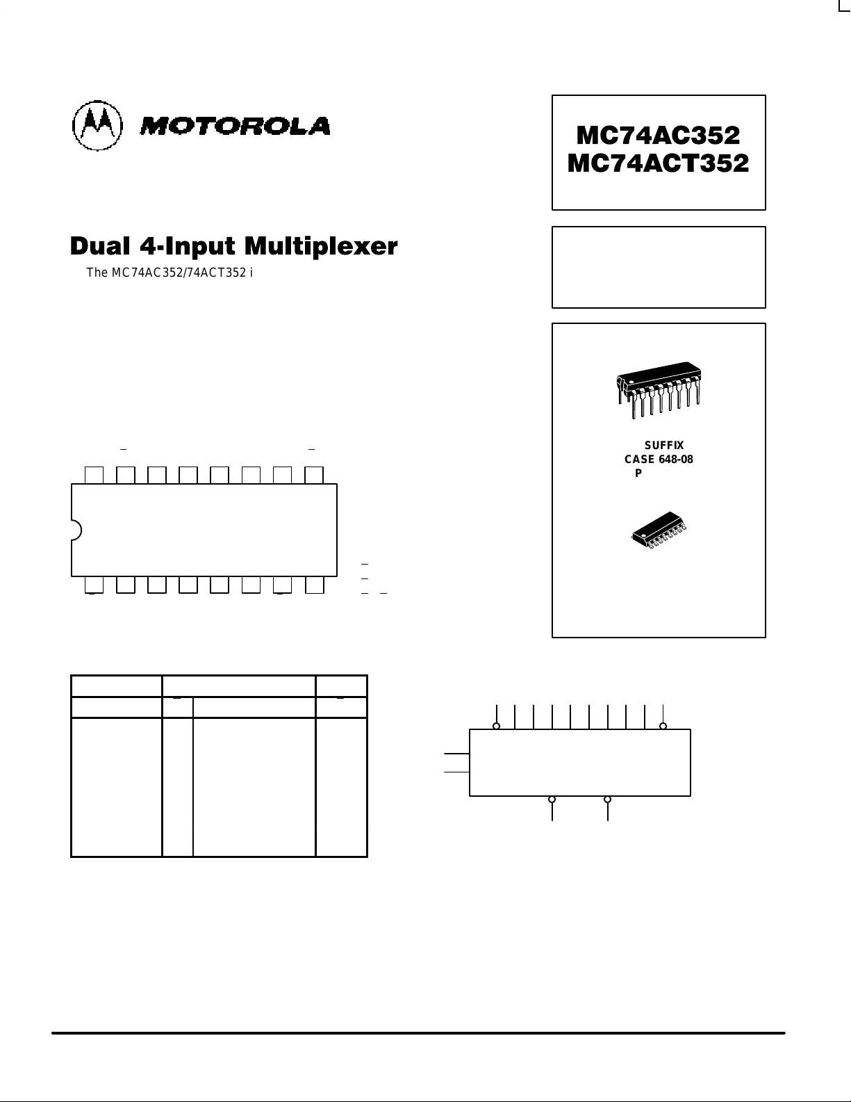
DUAL 4-INPUT
MULTIPLEXER
N SUFFIX
CASE 648-08
PLASTIC
D SUFFIX
CASE 751B-05
PLASTIC
LOGIC SYMBOL
S
0
S
1
EaI0aI1aI2aI
3a
Z
a
Z
b
I0bI1bI2bI3bE
b
MC74AC352 MC74ACT352
5-2
FACT DATA
FUNCTIONAL DESCRIPTION
The MC74AC352/74ACT352 is a dual 4-input multiplexer.
It selects two bits of data from up to four sources under the
control of the common Select inputs (S0, S1). The two 4-input
multiplexer circuits have individual active LOW Enables (E
a
,
E
b
) which can be used to strobe the outputs independently.
When the Enables (E
a
, Eb) are HIGH, the corresponding
outputs (Z
a
, Zb) are forced HIGH.
The logic equations for the outputs are shown below:
Z
a
= E
a
•(I0a•S1•S
0+I1a•S1
•S
0
+
I
2a
•S1•S
0+I3a
•S1•S
0
)
Z
b
= E
b
•(I0b•S1•S
0+I1b•S1
•S
0
+
I
2b
•S1•S
0+I3b
•S1•S
0
)
The MC74AC352/74ACT352 can be used to move data
from a group of registers to a common output bus. The
particular register from which the date came would be
determined by the state of the Select inputs. A less obvious
application is as a function generator. The MC74AC352/
74ACT352 can generate two functions of three variables. This
is useful for implementing highly irregular random logic.
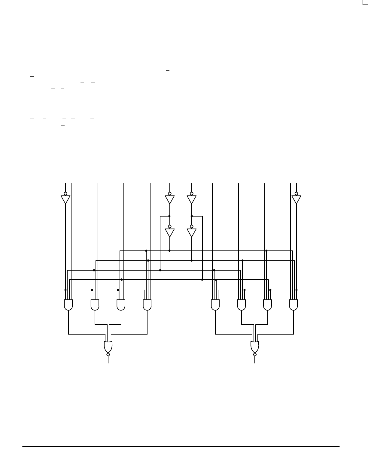
E
aI0a
I
3a
S
0
S
0
I
0b
I
1b
I
2b
I3bE
b
Z
a
Z
b
LOGIC DIAGRAM
Please note that this diagram is provided only for the understanding of logic
operations and should not be used to estimate propagation delays.
I
1a
I
2a
MC74AC352 MC74ACT352
5-3
FACT DATA
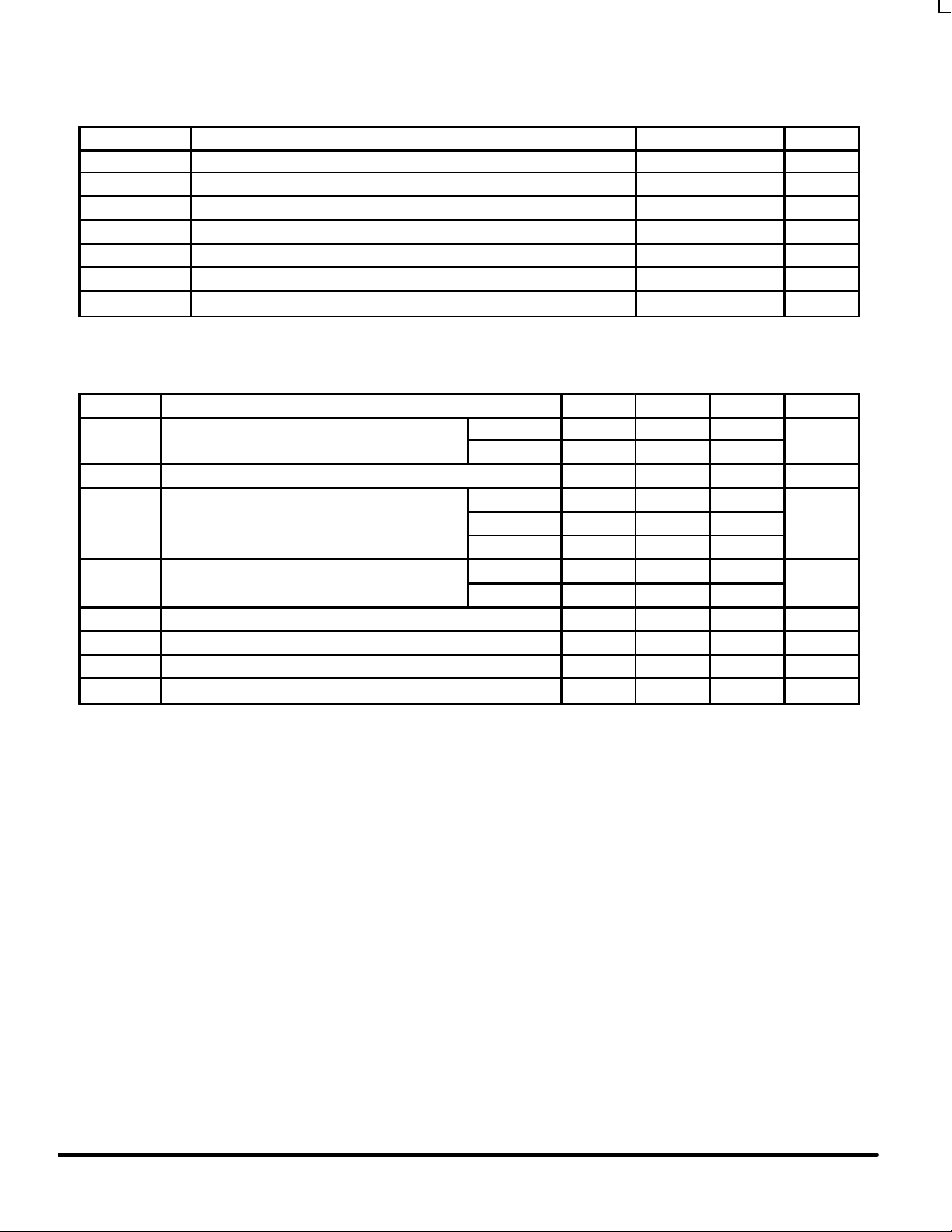
MAXIMUM RATINGS*
Symbol Parameter Value Unit
V
CC
DC Supply Voltage (Referenced to GND) –0.5 to +7.0 V
V
in
DC Input Voltage (Referenced to GND) –0.5 to VCC +0.5 V
V
out
DC Output Voltage (Referenced to GND) –0.5 to VCC +0.5 V
I
in
DC Input Current, per Pin ±20 mA
I
out
DC Output Sink/Source Current, per Pin ±50 mA
I
CC
DC VCC or GND Current per Output Pin ±50 mA
T
stg
Storage Temperature –65 to +150 °C
* Maximum Ratings are those values beyond which damage to the device may occur. Functional operation should be restricted to the Recommended
Operating Conditions.
RECOMMENDED OPERATING CONDITIONS
Symbol Parameter Min Typ Max Unit
′AC 2.0 5.0 6.0
VCCSupply Voltage
′ACT 4.5 5.0 5.5
V
Vin, V
out
DC Input Voltage, Output Voltage (Ref. to GND) 0 V
CC
V
VCC @ 3.0 V 150
Input Rise and Fall Time (Note 1)
′AC Devices except Schmitt Inputs
VCC @ 4.5 V 40 ns/V
r
, t
f
′AC Devices except Schmitt Inputs
VCC @ 5.5 V 25
VCC @ 4.5 V 10
tr, t
f
Input Rise and Fall Time (Note 2)
′ACT Devices except Schmitt Inputs
VCC @ 5.5 V 8.0
ns/V
T
J
Junction Temperature (PDIP) 140 °C
T
A
Operating Ambient Temperature Range –40 25 85 °C
I
OH
Output Current — High –24 mA
I
OL
Output Current — Low 24 mA
1. Vin from 30% to 70% VCC; see individual Data Sheets for devices that differ from the typical input rise and fall times.
2. Vin from 0.8 V to 2.0 V; see individual Data Sheets for devices that differ from the typical input rise and fall times.
tr, t
f
Input Rise and Fall Time (Note 2)
 Loading...