

Motorola MC74ACT350D, MC74AC350N, MC74AC350D, MC74ACT350N Datasheet
5-1
FACT DATA
The MC74AC350/74ACT350 is a specialized multiplexer that accepts a 4-bit
word and shifts it 0, 1, 2 or 3 places, as determined by two Select (S0, S1) inputs.
For expansion to longer words, three linking inputs are provided for lower-order
bits; thus two packages can shift an 8-bit word, four packages a 16-bit word, etc.
Shifting by more than three places is accomplished by paralleling the 3-state outputs
of different packages and using the Output Enable (OE
) inputs as a third Select
level. With appropriate interconnections, the ′AC/ACT350 can perform zero-backfill,
sign-extend or end-around (barrel) shift functions.
• Linking Inputs for Word Expansion
• 3-State Outputs for Extending Shift Range
1516 14 13 12 11 10
21 3 4 5 6 7
V
CC
9
8
O0O1OE O2O3S0S
1
I
–3I–2I–1I0I1I2I3
GND
TRUTH TABLE
Inputs Outputs
OE S
1
S
0
O
0
O
1
O
2
O
3
H X X Z Z Z Z
L L L I
0
I
1
I
2
I
3
L L H I
–1
I
0
I
1
I
2
L H L I
–2
I
–1
I
0
I
1
L H H I
–3
I
–2
I
–1
I
0
H = HIGH Voltage Level
L = LOW Voltage Level
X = Immaterial
4-BIT SHIFTER
WITH 3-STATE
OUTPUTS
N SUFFIX
CASE 648-08
PLASTIC
D SUFFIX
CASE 751B-05
PLASTIC
LOGIC SYMBOL
OE
S
1
S
0
O0O1O2O
3
I–3I–2I–1I0I1I2I
3
13
9
10
15 14 12 11
1 2 3 4 5 6 7
MC74AC350 MC74ACT350
5-2
FACT DATA
FUNCTIONAL DESCRIPTION
The MC74AC350/74ACT350 is operationally equivalent to
a 4-input multiplexer with the inputs connected so that the
select code causes successive one-bit shifts of the data word.
This internal connection makes it possible to perform shifts of
0, 1, 2 or 3 places on words of any length.
A 7-bit data word is introduced at the In inputs and is shifted
according to the code applied to the select inputs S0, S1.
Outputs O0–O3 are 3-state, controlled by an active-LOW
output enable (OE
). When OE is LOW, data outputs will follow
selected data inputs; when HIGH, the data outputs will be
forced to the high-impedance state. This feature allows
shifters to be cascaded on the same output lines or to a
common bus. The shift function can be logical, with zeros
pulled in at either or both ends of the shifting field; arithmetic,
where the sign bit is repeated during a shift down; or end
around, where the data word forms a continuous loop.
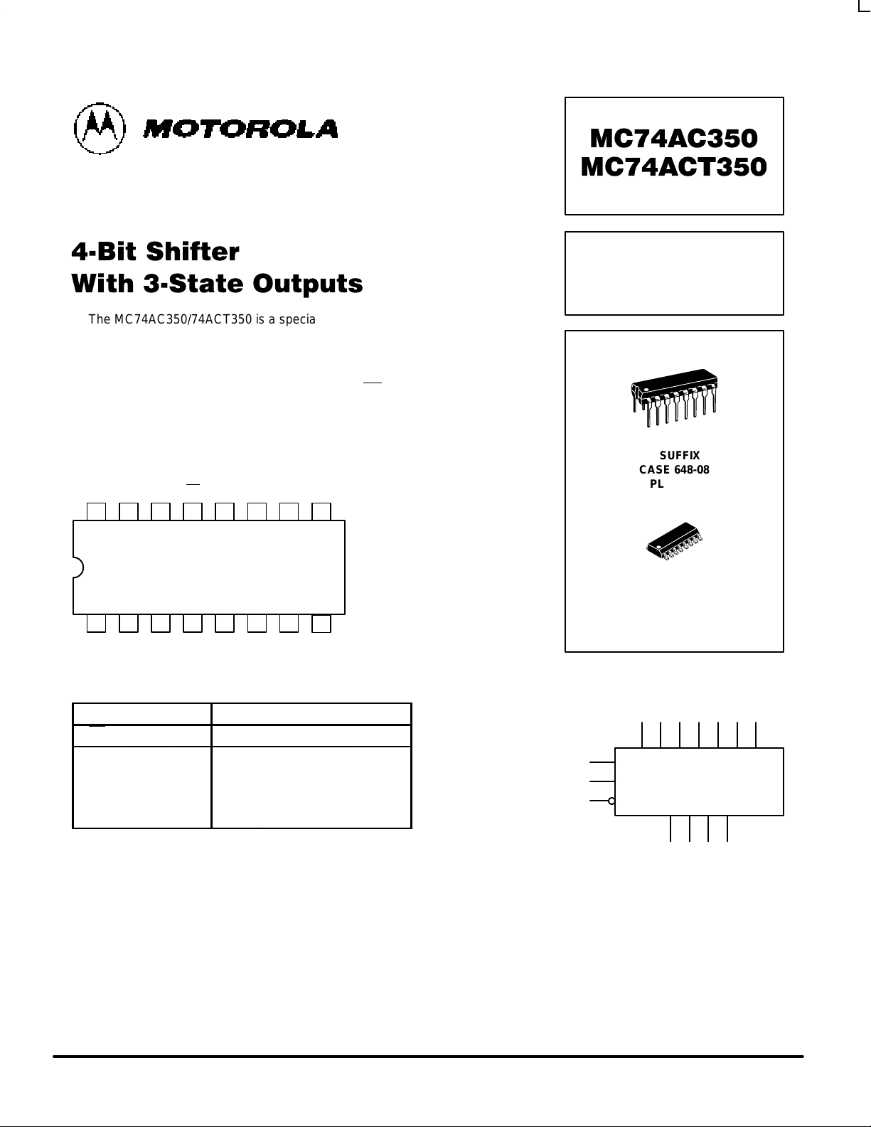
LOGIC EQUATIONS
O0=S
0 S1 I0+S0 S1 I–1+S0 S1 I–2+S0 S1 I–3
O1=S
0 S1 I1+S0 S1 I0+S0 S1 I–1+S0 S1 II–2
O2=S
0 S1 I2+S0 S1 I1+S0 S1 I0+S0 S1 I–1
O3=S
0 S1 I3+S0 S1 I2+S0 S1 I1+S0 S1 I0
LOGIC DIAGRAM
I
–3
I
–2
I
–1
I0I1I2I
3
S
1
S0OE
O
0
O
1
O
2
O
3
MC74AC350 MC74ACT350
5-3
FACT DATA
APPLICATIONS
16-Bit Shift-Up 0 to 3 Places, Zero Backfill
GND
S
0
S
1
OE
S
0
S
1
OE
Y0Y1Y2Y
3
I–3I–1I0I1I2I
3
I
–2
S
0
S
1
OE
Y0Y1Y2Y
3
I–3I–1I0I1I2I
3
I
–2
S
0
S
1
OE
Y0Y1Y2Y
3
I–3I–1I0I1I2I
3
I
–2
S
0
S
1
OE
Y0Y1Y2Y
0
I–3I–1I0I1I2I
3
I
–2
0 1 2 3 4 5 6 7 8 9 10 11 12 13 14 15
0 1 2 3 4 5 6 7 8 9 10 11 12 13 14 15
S1S
0
L L NO SHIFT
L H SHIFT 1 PLACE
H L SHIFT 2 PLACES
H H SHIFT 3 PLACES
S
0
S
1
S
2
S
0
S
1
OE
Y0Y1Y2Y
3
I–3I–1I0I1I2I
3
I
–2
S
0
S
1
OE
Y0Y1Y2Y
3
I–3I–1I0I1I2I
3
I
–2
S
0
S
1
OE
Y0Y1Y2Y
3
I–3I–1I0I1I2I
3
I
–2
S
0
S
1
OE
Y0Y1Y2Y
3
I–3I–1I0I1I2I
3
I
–2
0 1 2 3 4 5 6 7
0 1 2 3 4 5 6 7
S
2
8-Bit End Around Shift 0 to 7 Places
S2S1S
0
S2S1S
0
L L L NO SHIFT H L H SHIFT END AROUND 5
L L H SHIFT END AROUND 1 H H L SHIFT END AROUND 6
L H L SHIFT END AROUND 2 H H H SHIFT END AROUND 7
L H H SHIFT END AROUND 3
H L L SHIFT END AROUND 4
 Loading...