

MOTOROLA MC74ACT299DW, MC74ACT299DWR2, MC74ACT299N, MC74AC299N, MC74AC299DWR2 Datasheet
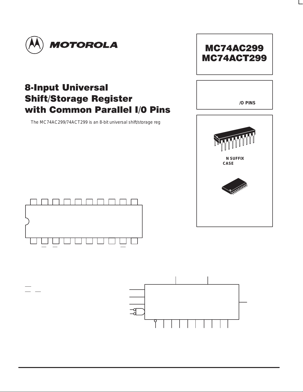
MC74AC299
MC74ACT299
8ĆInput Universal
Shift/Storage Register
with Common Parallel I/0 Pins
The MC74AC299/74ACT299 is an 8-bit universal shift/storage register
with 3-state outputs. Four modes of operation are possible: hold (store), shift left,
shift right and load data. The parallel load inputs and flip-flop outputs are multiplexed
to reduce the total number of package pins. Additional outputs are provided for
flip-flops Q0, Q7 to allow easy serial cascading. A separate active LOW Master
Reset is used to reset the register.
• Common Parallel I/O for Reduced Pin Count
• Additional Serial Inputs and Outputs for Expansion
• Four Operating Modes: Shift Left, Shift Right, Load and Store
• 3-State Outputs for Bus-Oriented Applications
• Outputs Source/Sink 24 mA
•′ACT299 Has TTL Compatible Inputs
S1DS7Q7I/O7I/O5I/O3I/O1CP DS
V
CC
1920 18 17 16 15 14
13
0
12
11
8-INPUT UNIVERSAL
SHIFT/STORAGE REGISTER
WITH COMMON
PARALLEL I/O PINS
N SUFFIX
CASE 738-03
PLASTIC
DW SUFFIX
CASE 751D-04
PLASTIC
21 34567
S0OE
1OE2
PIN NAMES
CP Clock Pulse Input
DS
0
DS
7
S0, S
MR Asynchronous Master Reset
OE
OE23-State Output Enable Inputs
1,
I/O0–I/O7Parallel Data Inputs or
Q0, Q
Serial Data Input for Right Shift
Serial Data Input for Left Shift
Mode Select Inputs
1
3-State Parallel Outputs
Serial Outputs
7
I/O6I/O4I/O2I/O0Q0MR GND
9
8
10
LOGIC SYMBOL
S
0
S
1
CP
OE
MR Q0I/O
DS
0
I/O
I/O
DS
7
Q
7
I/O
I/O
I/O
4
3
I/O
6
5
7
0
I/O
2
1
FACT DAT A
5-1
MC74AC299 MC74ACT299
LOGIC DIAGRAM
DS
7
Q
7
DQ
C
D
CP
DQ
C
D
CP
DQ
C
D
CP
DQ
C
D
CP
DQ
C
D
I/O
7
I/O
6
I/O
5
I/O
4
I/O
3
CP
DQ
C
D
CP
DQ
C
D
CP
DQ
C
D
S
0
S
1
DS
0
CP
Q0MR
OE
1
Please note that this diagram is provided only for the understanding of logic
operations and should not be used to estimate propagation delays.
I/O
2
I/O
1
I/O
0
OE
2
FACT DAT A
5-2
FUNCTIONAL DESCRIPTION
Response
VCCSupply Voltage
V
AC Devices exce t Schmitt In uts
t
t
()
ns/V
MC74AC299 MC74ACT299
The MC74AC299/74ACT299 contains eight edge-triggered
D-type flip-flops and the interstage logic necessary to perform
synchronous shift left, shift right, parallel load and hold
operations. The type of operation is determined by S0 and S1,
as shown in the Truth T able. All flip-flop outputs are brought out
through 3-state buffers to separate I/O pins that also serve as
data inputs in the parallel load mode. Q0 and Q7 are also
brought out on other pins for expansion in serial shifting of
longer words.
A LOW signal on MR
overrides the Select and CP inputs
and resets the flip-flops. All other state changes are initiated
by the rising edge of the clock. Inputs can change when the
clock is in either state provided only that the recommended
setup and hold times, relative to the rising edge of CP, are
TRUTH TABLE
Inputs
MR S1S0CP
L X X X Asynchronous Reset; Q0–Q7 = LOW
H H H Parallel Load; I/On Q
H L H Shift Rights; DS0 Q0, Q0 Q1, etc.
H H L Shift Left; DS7 Q7, Q7 Q6, etc.
H L L X Hold
H = HIGH Voltage Level
L = LOW Voltage Level
X = Immaterial
= LOW-to-HIGH Transition
n
observed.
A HIGH signal on either OE
or OE2 disables the 3-state
1
buffers and puts the I/O pins in the high impedance state. In
this condition the shift, hold, load and reset operations can still
occur. The 3-state buffers are also disabled by HIGH signals
on both S0 and S1 in preparation for a parallel load operation.
MAXIMUM RATINGS*
Symbol Parameter Value Unit
V
CC
V
in
V
out
I
in
I
out
I
CC
T
stg
* Maximum Ratings are those values beyond which damage to the device may occur. Functional operation should be restricted to the Recommended
Operating Conditions.
DC Supply Voltage (Referenced to GND) –0.5 to +7.0 V
DC Input Voltage (Referenced to GND) –0.5 to VCC +0.5 V
DC Output Voltage (Referenced to GND) –0.5 to VCC +0.5 V
DC Input Current, per Pin ±20 mA
DC Output Sink/Source Current, per Pin ±50 mA
DC VCC or GND Current per Output Pin ±50 mA
Storage Temperature –65 to +150 °C
RECOMMENDED OPERATING CONDITIONS
Symbol Parameter Min Typ Max Unit
Vin, V
out
tr, t
f
,
r
f
T
J
T
A
I
OH
I
OL
1. Vin from 30% to 70% VCC; see individual Data Sheets for devices that differ from the typical input rise and fall times.
2. Vin from 0.8 V to 2.0 V; see individual Data Sheets for devices that differ from the typical input rise and fall times.
DC Input Voltage, Output Voltage (Ref. to GND) 0 V
Input Rise and Fall Time (Note 1)
′AC Devices except Schmitt Inputs
Input Rise and Fall Time (Note 2)
′ACT Devices except Schmitt Inputs
Junction Temperature (PDIP) 140 °C
Operating Ambient Temperature Range –40 25 85 °C
Output Current — High –24 mA
Output Current — Low 24 mA
pp
VCC @ 3.0 V 150
VCC @ 4.5 V 40 ns/V
VCC @ 5.5 V 25
VCC @ 4.5 V 10
VCC @ 5.5 V 8.0
FACT DAT A
5-3
′AC 2.0 5.0 6.0
′ACT 4.5 5.0 5.5
CC
V
 Loading...