

5-1
FACT DATA
The MC74AC259/74ACT259 is a high-speed 8-bit addressable latch designed for
general purpose storage applications in digital systems. It is a multifunctional device
capable of storing single line data in eight addressable latches, and also a 1-of-8
decoder and demultiplexer with active HIGH outputs. The device also incorporates
an active LOW Common Clear for resetting all latches, as well as an active LOW
Enable. It is functionally identical to the ALS259 8-bit addressable latch.
• Serial-to-Parallel Conversion
• Eight Bits of Storage with Output of Each Bit Available
• Random (Addressable) Data Entry
• Active High Demultiplexing or Decoding Capability
• Easily Expandable
• Common Clear
FUNCTIONAL DESCRIPTION
The MC74AC259/74ACT259 has four modes of operation as shown in the Mode
Selection Table. In the addressable latch mode, data on the Data line (D) is written
into the addressed latch. The addressed latch will follow the data input with all nonaddressed latches remaining in their previous states in the memory mode. All latches
remain in their previous state and are unaffected by the Data or Address inputs.
In the one-of-eight decoding or demultiplexing mode, the addressed output will
follow the state of the D input with all other outputs in the LOW state. In the clear
mode all outputs are LOW and unaffected by the address and data inputs. When
operating the MC74AC/ACT259 as an addressable latch, changing more than one
bit of the address could impose a transient wrong address. Therefore, this should
only be done while in the memory mode. The Mode Select Function Table
summarizes the operations of the MC74AC/ACT259.
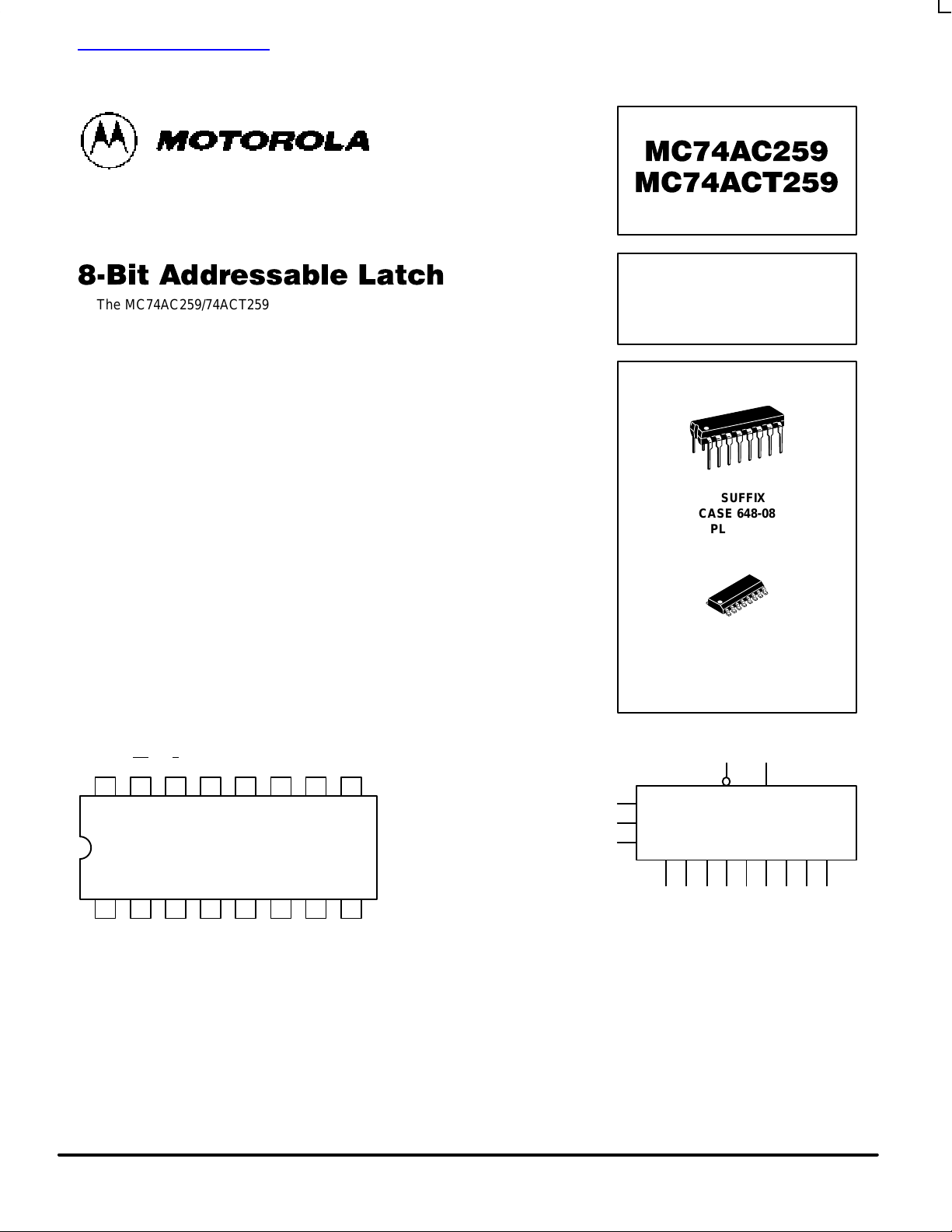
8-BIT
ADDRESSABLE
LATCH
N SUFFIX
CASE 648-08
PLASTIC
D SUFFIX
CASE 751B-05
PLASTIC
LOGIC SYMBOL
A
0
A
1
A
2
E D
MR Q0Q1Q2Q3Q4Q5Q6Q
7
1516 14 13 12 11 10
21 3 4 5 6 7
V
CC
9
8
MR E D Q7Q6Q5Q
4
A0A1A2Q0Q1Q2Q3GND
查询MC74AC259供应商
MC74AC259 MC74ACT259
5-2
FACT DATA
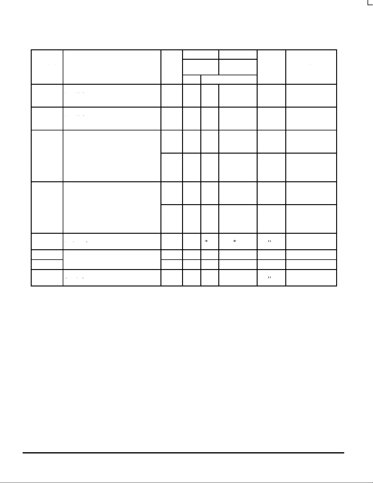
MODE SELECT TABLE
E MR Mode
L H Addressable Latch
H H Memory
L L Active HIGH 8-Channel Demultiplexer
H L Clear
H = HIGH Voltage Level
L = LOW Voltage Level
MODE SELECT-FUNCTION TABLE
Operating
Inputs Outputs
Operating
Mode
MR E D A0A1A2Q
0
Q
1
Q
2
Q
3
Q
4
Q
5
Q
6
Q
7
Master Reset L H X X X X L L L L L L L L
L L d L L L Q = d L L L L L L L
L L d H L L L Q = d L L L L L L
Demultiplex
L L d L H L L L Q = d L L L L L
(Active HIGH
• • • • • • • • • • • • • •
Decoder when
D = H)
• • • • • • • • • • • • • •
D = H)
• • • • • • • • • • • • • •
L L d H H H L L L L L L L Q = d
HHXXXXq0q1q2q3q4q5q6q
7
H L d L L L Q = d q
1
q
2
q
3
q
4
q
5
q
6
q
7
H L d H L L q0Q = d q
2
q
3
q
4
q
5
q
6
q
7
H L d L H L q
0
q1Q = d q
3
q
4
q
5
q
6
q
7
Addressable
• • • • • • • • • • • • • •
Latch
• • • • • • • • • • • • • •
• • • • • • • • • • • • • •
H L d H H H q
0
q
1
q
2
q
3
q
4
q
5
q6Q = d
H = HIGH Voltage Level
L = LOW Voltage Level
X = Immaterial
d = HIGH or LOW Data one setup time prior to the LOW-to-HIGH Enable transition
q = Lower case letters indicate the state of the referenced output established during the last cycle in which it was addressed
or cleared.
Store
(Do Nothing)
MC74AC259 MC74ACT259
5-3
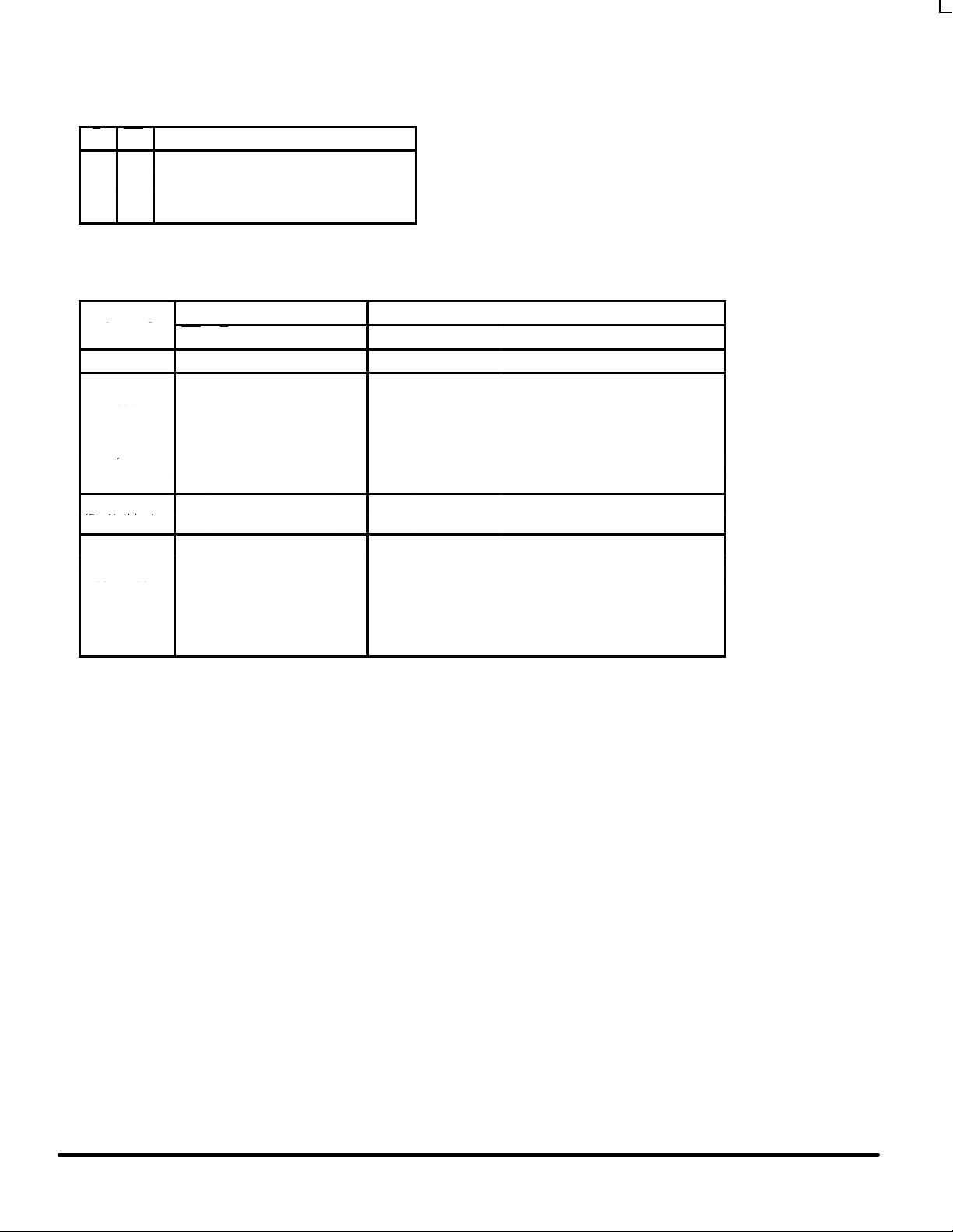
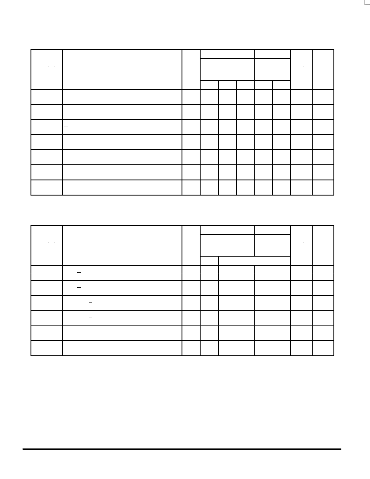
FACT DATA
MR
A
2
A
1
A
0
D
E
Q
7
Q
6
Q
5
Q
4
Q
3
Q
2
Q
1
Q
0
Please note that this diagram is provided only for the understanding of logic
operations and should not be used to estimate propagation delays.
MC74AC259 MC74ACT259
5-4
FACT DATA
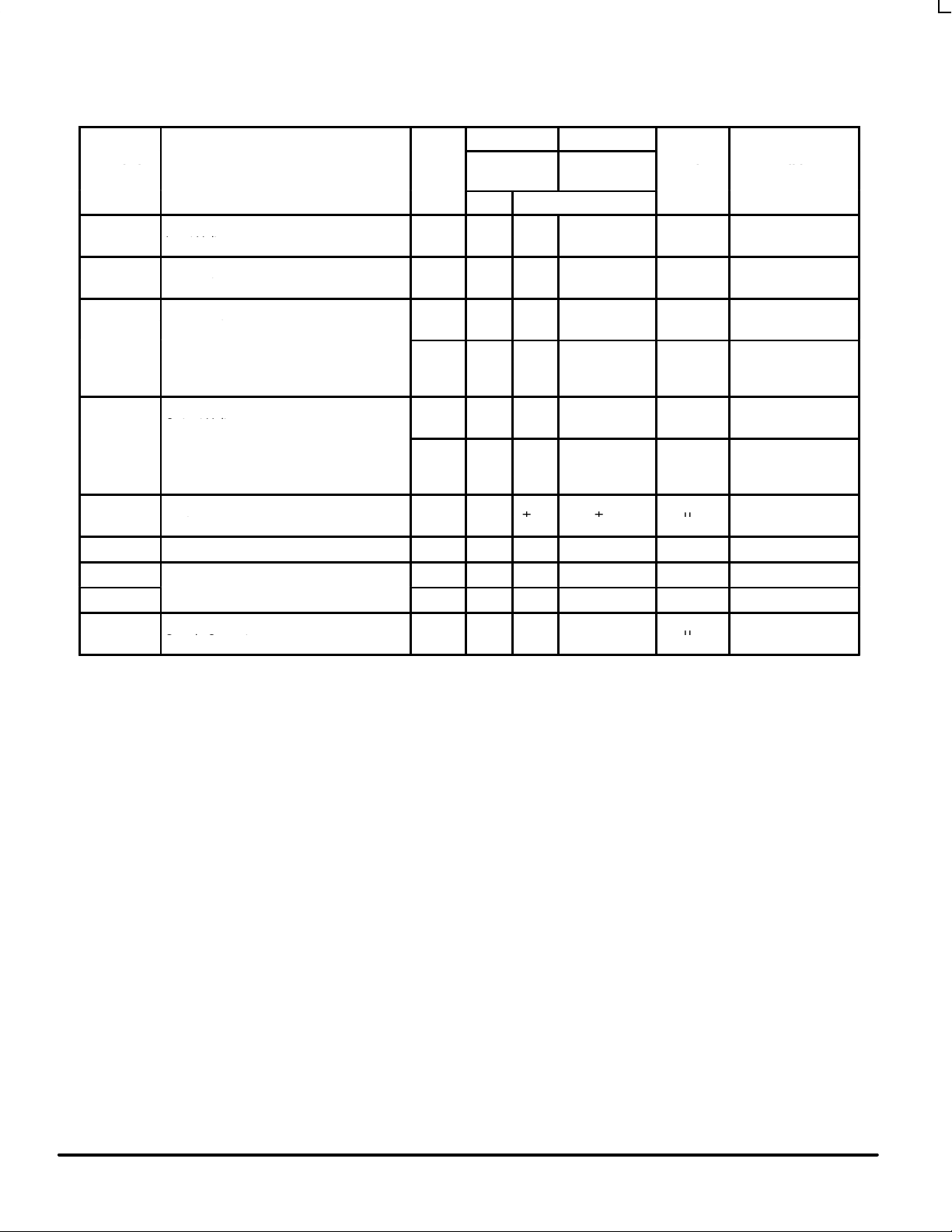
MAXIMUM RATINGS*
Symbol Parameter Value Unit
V
CC
DC Supply Voltage (Referenced to GND) –0.5 to +7.0 V
V
in
DC Input Voltage (Referenced to GND) –0.5 to VCC +0.5 V
V
out
DC Output Voltage (Referenced to GND) –0.5 to VCC +0.5 V
I
in
DC Input Current, per Pin ±20 mA
I
out
DC Output Sink/Source Current, per Pin ±50 mA
I
CC
DC VCC or GND Current per Output Pin ±50 mA
T
stg
Storage Temperature –65 to +150 °C
* Maximum Ratings are those values beyond which damage to the device may occur. Functional operation should be restricted to the Recommended
Operating Conditions.
RECOMMENDED OPERATING CONDITIONS
Symbol Parameter Min Typ Max Unit
′AC 2.0 5.0 6.0
VCCSupply Voltage
′ACT 4.5 5.0 5.5
V
Vin, V
out
DC Input Voltage, Output Voltage (Ref. to GND) 0 V
CC
V
VCC @ 3.0 V 150
Input Rise and Fall Time (Note 1)
′AC Devices except Schmitt Inputs
VCC @ 4.5 V 40 ns/V
r
, t
f
′AC Devices except Schmitt Inputs
VCC @ 5.5 V 25
VCC @ 4.5 V 10
tr, t
f
Input Rise and Fall Time (Note 2)
′ACT Devices except Schmitt Inputs
VCC @ 5.5 V 8.0
ns/V
T
J
Junction Temperature (PDIP) 140 °C
T
A
Operating Ambient Temperature Range –40 25 85 °C
I
OH
Output Current — High –24 mA
I
OL
Output Current — Low 24 mA
1. Vin from 30% to 70% VCC; see individual Data Sheets for devices that differ from the typical input rise and fall times.
2. Vin from 0.8 V to 2.0 V; see individual Data Sheets for devices that differ from the typical input rise and fall times.
tr, t
f
Input Rise and Fall Time (Note 2)
MC74AC259 MC74ACT259
5-5
FACT DATA
DC CHARACTERISTICS
74AC 74AC
Symbol
Parameter
V
CC
(V)
TA = +25°C
TA =
–40°C to +85°C
Unit
Conditions
Typ Guaranteed Limits
V
IH
3.0 1.5 2.1 2.1 V
OUT
= 0.1 V
4.5 2.25 3.15 3.15 V or VCC – 0.1 V
5.5 2.75 3.85 3.85
V
IL
3.0 1.5 0.9 0.9 V
OUT
= 0.1 V
4.5 2.25 1.35 1.35 V or VCC – 0.1 V
5.5 2.75 1.65 1.65
V
OH
3.0 2.99 2.9 2.9 I
OUT
= –50 µA
4.5 4.49 4.4 4.4 V
5.5 5.49 5.4 5.4
*VIN = VIL or V
IH
3.0 2.56 2.46
–12 mA
4.5 3.86 3.76
V
I
OH
–24 mA
5.5 4.86 4.76 –24 mA
V
OL
3.0 0.002 0.1 0.1 I
OUT
= 50 µA
4.5 0.001 0.1 0.1 V
5.5 0.001 0.1 0.1
*VIN = VIL or V
IH
3.0 0.36 0.44
12 mA
4.5 0.36 0.44
V
I
OL
24 mA
5.5 0.36 0.44 24 mA
I
IN
5.5
±0.1
±1.0
µA
VI = VCC, GND
I
OLD
5.5 75 mA V
OLD
= 1.65 V Max
I
OHD
Output Current
5.5 –75 mA V
OHD
= 3.85 V Min
I
CC
5.5
8.080µA
VIN = VCC or GND
* All outputs loaded; thresholds on input associated with output under test.
†Maximum test duration 2.0 ms, one output loaded at a time.
Note: IIN and ICC @ 3.0 V are guaranteed to be less than or equal to the respective limit @ 5.5 V VCC.
Minimum High Level
Input Voltage
Maximum Low Level
Input Voltage
Minimum High Level
Output Voltage
Maximum Low Level
Output Voltage
Maximum Input
Leakage Current
†Minimum Dynamic
Maximum Quiescent
Supply Current
MC74AC259 MC74ACT259
5-6
FACT DATA
AC CHARACTERISTICS (For Figures and Waveforms — See Section 3)
74AC 74AC
Symbol
Parameter
VCC*
(V)
TA = +25°C
CL = 50 pF
TA = –40°C
to +85°C
CL = 50 pF
Unit
Fig.
No.
Min Typ Max Min Max
Propagation Delay
3.3 2.0 9.0 14.5 1.5 17.0
t
PLH
Dn to Q
n
5.0 2.0 6.5 10.0 1.5 11.5
ns
3-5
Propagation Delay
3.3 2.0 9.0 13.5 1.5 16.0
t
PHL
Dn to Q
n
5.0 2.0 6.0 9.5 1.5 11.0
ns
3-5
Propagation Delay
3.3 2.0 10.5 15.0 1.5 17.5
t
PLH
E to Q
n
5.0 2.0 7.0 10.5 1.5 12.5
ns
3-6
Propagation Delay
3.3 2.0 8.0 12.5 1.5 15.0
t
PHL
E to Q
n
5.0 2.0 7.5 9.0 1.5 11.0
ns
3-6
Propagation Delay
3.3 2.0 12.0 19.0 1.5 22.5
t
PLH
Address to Q
n
5.0 2.0 8.0 13.0 1.5 15.5
ns
3-6
Propagation Delay
3.3 2.0 10.0 16.0 1.5 19.0
t
PHL
Address to Q
n
5.0 2.0 7.0 11.0 1.5 13.0
ns
3-6
Propagation Delay
3.3 2.0 8.0 12.0 1.5 13.5
t
PHL
MR to Q 5.0 2.0 6.0 9.0 1.5 10.0
ns
3-7
* Voltage Range 3.3 V is 3.3 V ±0.3 V.
Voltage Range 5.0 V is 5.0 V ±0.5 V.
AC OPERATING REQUIREMENTS
74AC 74AC
Symbol
Parameter
VCC*
(V)
TA = +25°C
CL = 50 pF
TA = –40°C
to +85°C
CL = 50 pF
Unit
Fig.
No.
Typ Guaranteed Minimum
Setup Time, HIGH or LOW 3.3 3.5 4.5
t
s
Dn to E 5.0 2.5 3.5
ns
3-9
Hold Time, HIGH or LOW 3.3 2.5 2.5
t
h
Dn to E 5.0 2.0 2.0
ns
3-9
Setup Time 3.3 7.0 9.0
t
s
Address to E 5.0 4.0 6.0
ns
3-6
Hold Time 3.3 2.0 2.0
t
h
Address to E 5.0 2.0 2.0
ns
3-6
Minimum Pulse 3.3 6.0 6.5
t
w
Width MR 5.0 5.5 6.0
ns
3-6
Minimum Pulse 3.3 6.5 7.0
t
w
Width E 5.0 5.5 6.0
ns
3-6
* Voltage Range 3.3 V is 3.3 V ±0.3 V.
Voltage Range 5.0 V is 5.0 V ±0.5 V.
MC74AC259 MC74ACT259
5-7
FACT DATA
DC CHARACTERISTICS
74ACT 74ACT
Symbol
Parameter
V
CC
(V)
TA = +25°C
TA =
–40°C to +85°C
Unit
Conditions
Typ Guaranteed Limits
V
IH
4.5 1.5 2.0 2.0
V
OUT
= 0.1 V
5.5 1.5 2.0 2.0
V
or VCC – 0.1 V
V
IL
4.5 1.5 0.8 0.8
V
OUT
= 0.1 V
5.5 1.5 0.8 0.8
V
or VCC – 0.1 V
V
OH
4.5 4.49 4.4 4.4
I
OUT
= –50 µA
5.5 5.49 5.4 5.4
V
*VIN = VIL or V
IH
4.5 3.86 3.76 V
–24 mA
5.5 4.86 4.76
I
OH
–24 mA
V
OL
4.5 0.001 0.1 0.1
I
OUT
= 50 µA
5.5 0.001 0.1 0.1
V
*VIN = VIL or V
IH
4.5 0.36 0.44 V
24 mA
5.5 0.36 0.44
I
OL
24 mA
I
IN
5.5
±0.1
±1.0
µA
VI = VCC, GND
∆I
CCT
Additional Max. ICC/Input 5.5 0.6 1.5 mA VI = VCC – 2.1 V
I
OLD
5.5 75 mA V
OLD
= 1.65 V Max
I
OHD
Output Current
5.5 –75 mA V
OHD
= 3.85 V Min
I
CC
5.5
8.080µA
VIN = VCC or GND
* All outputs loaded; thresholds on input associated with output under test.
†Maximum test duration 2.0 ms, one output loaded at a time.
Minimum High Level
Input Voltage
Maximum Low Level
Input Voltage
Minimum High Level
Output Voltage
Maximum Low Level
Output Voltage
Maximum Input
Leakage Current
†Minimum Dynamic
Maximum Quiescent
Supply Current
MC74AC259 MC74ACT259
5-8
FACT DATA
AC CHARACTERISTICS (For Figures and Waveforms — See Section 3)
74ACT 74ACT
Symbol
Parameter
VCC*
(V)
TA = +25°C
CL = 50 pF
TA = –40°C
to +85°C
CL = 50 pF
Unit
Fig.
No.
Min Typ Max Min Max
t
PLH
5.0
2.0
6.5
11.0
1.5
12.5ns3-5
t
PHL
5.0
2.0
7.0
10.5
1.5
12.0ns3-5
t
PLH
to Q
n
5.0
2.0
10.5
14.0
1.5
16.5ns3-6
t
PHL
or Q
n
5.0
2.0
9.0
12.0
1.5
14.0ns3-6
t
PLH
5.0
2.0
8.0
11.5
1.5
13.5ns3-6
t
PHL
5.0
2.0
6.0
10.0
1.5
12.0ns3-6
t
PHL
to Q
5.0
2.0
10.0
1.5
11.0ns3-7
* Voltage Range 5.0 V is 5.0 V ±0.5 V.
AC OPERATING REQUIREMENTS
74ACT 74ACT
Symbol
Parameter
VCC*
(V)
TA = +25°C
CL = 50 pF
TA = –40°C
to +85°C
CL = 50 pF
Unit
Fig.
No.
Typ Guaranteed Minimum
t
s
5.0
3.0
4.0
ns
3-9
t
h
5.0
2.5
2.5
ns
3-9
t
s
5.0
4.5
6.5
ns
3-6
t
h
5.0
2.5
2.5
ns
3-6
Minimum Pulse
t
w
Width MR
5.0
7.0
7.5
ns
3-6
Minimum Pulse
t
w
Width E
5.0
7.0
7.5
ns
3-6
* Voltage Range 5.0 V is 5.0 V ±0.5 V.
CAPACITANCE
Symbol Parameter
Value
Typ
Unit Test Conditions
C
IN
Input Capacitance 4.5 pF VCC = 5.0 V
C
PD
Power Dissipation Capacitance 50.0 pF VCC = 5.0 V
Propagation Delay
Dn to Q
n
Propagation Delay
Dn or Q
n
Propagation Delay
E
Propagation Delay
E
Propagation Delay
Address to Q
Propagation Delay
Address to Q
Propagation Delay
MR
n
n
Setup Time, HIGH or LOW
Dn to E
Hold Time, HIGH or LOW
Dn to E
Setup Time
Address to E
Hold Time
Address to E

MC74AC259 MC74ACT259
5-9
FACT DATA
OUTLINE DIMENSIONS
N SUFFIX
PLASTIC DIP PACKAGE
CASE 648–08
ISSUE R
D SUFFIX
PLASTIC SOIC PACKAGE
CASE 751B–05
ISSUE J
NOTES:
1. DIMENSIONING AND TOLERANCING PER
ANSI Y14.5M, 1982.
2. CONTROLLING DIMENSION: MILLIMETER.
3. DIMENSIONS A AND B DO NOT INCLUDE
MOLD PROTRUSION.
4. MAXIMUM MOLD PROTRUSION 0.15 (0.006)
PER SIDE.
5. DIMENSION D DOES NOT INCLUDE DAMBAR
PROTRUSION. ALLOWABLE DAMBAR
PROTRUSION SHALL BE 0.127 (0.005) TOTAL
IN EXCESS OF THE D DIMENSION AT
MAXIMUM MATERIAL CONDITION.
1 8
16 9
SEATING
PLANE
F
J
M
R
X 45
_
G
8 PLP
–B–
–A–
M
0.25 (0.010) B
S
–T–
D
K
C
16 PL
S
B
M
0.25 (0.010) A
S
T
DIM MIN MAX MIN MAX
INCHESMILLIMETERS
A 9.80 10.00 0.386 0.393
B 3.80 4.00 0.150 0.157
C 1.35 1.75 0.054 0.068
D 0.35 0.49 0.014 0.019
F 0.40 1.25 0.016 0.049
G 1.27 BSC 0.050 BSC
J 0.19 0.25 0.008 0.009
K 0.10 0.25 0.004 0.009
M 0 7 0 7
P 5.80 6.20 0.229 0.244
R 0.25 0.50 0.010 0.019
_ _ _ _
NOTES:
1. DIMENSIONING AND TOLERANCING PER ANSI
Y14.5M, 1982.
2. CONTROLLING DIMENSION: INCH.
3. DIMENSION L TO CENTER OF LEADS WHEN
FORMED PARALLEL.
4. DIMENSION B DOES NOT INCLUDE MOLD FLASH.
5. ROUNDED CORNERS OPTIONAL.
–A–
B
F
C
S
H
G
D
J
L
M
16 PL
SEATING
1 8
916
K
PLANE
–T–
M
A
M
0.25 (0.010) T
DIM MIN MAX MIN MAX
MILLIMETERSINCHES
A 0.740 0.770 18.80 19.55
B 0.250 0.270 6.35 6.85
C 0.145 0.175 3.69 4.44
D 0.015 0.021 0.39 0.53
F 0.040 0.70 1.02 1.77
G 0.100 BSC 2.54 BSC
H 0.050 BSC 1.27 BSC
J 0.008 0.015 0.21 0.38
K 0.110 0.130 2.80 3.30
L 0.295 0.305 7.50 7.74
M 0 10 0 10
S 0.020 0.040 0.51 1.01
____
How to reach us:
USA/EUROPE: Motorola Literature Distribution; JAPAN: Nippon Motorola Ltd.; Tatsumi–SPD–JLDC, Toshikatsu Otsuki,
P.O. Box 20912; Phoenix, Arizona 85036. 1–800–441–2447 6F Seibu–Butsuryu–Center, 3–14–2 Tatsumi Koto–Ku, Tokyo 135, Japan. 03–3521–8315
MFAX: RMFAX0@email.sps.mot.com –TOUCHTONE (602) 244–6609 HONG KONG: Motorola Semiconductors H.K. Ltd.; 8B Tai Ping Industrial Park,
INTERNET: http://Design–NET.com 51 Ting Kok Road, Tai Po, N.T., Hong Kong. 852–26629298
Motorola reserves the right to make changes without further notice to any products herein. Motorola makes no warranty , representation or guarantee regarding
the suitability of its products for any particular purpose, nor does Motorola assume any liability arising out of the application or use of any product or circuit, and
specifically disclaims any and all liability , including without limitation consequential or incidental damages. “Typical” parameters can and do vary in different
applications. All operating parameters, including “T ypicals” must be validated for each customer application by customer’s technical experts. Motorola does
not convey any license under its patent rights nor the rights of others. Motorola products are not designed, intended, or authorized for use as components in
systems intended for surgical implant into the body, or other applications intended to support or sustain life, or for any other application in which the failure of
the Motorola product could create a situation where personal injury or death may occur. Should Buyer purchase or use Motorola products for any such
unintended or unauthorized application, Buyer shall indemnify and hold Motorola and its officers, employees, subsidiaries, affiliates, and distributors harmless
against all claims, costs, damages, and expenses, and reasonable attorney fees arising out of, directly or indirectly, any claim of personal injury or death
associated with such unintended or unauthorized use, even if such claim alleges that Motorola was negligent regarding the design or manufacture of the part.
Motorola and are registered trademarks of Motorola, Inc. Motorola, Inc. is an Equal Opportunity/Affirmative Action Employer.
MC74AC259/D
*MC74AC259/D*
◊
 Loading...