

Motorola MC74ACT258D, MC74ACT258N, MC74AC258D, MC74AC258N Datasheet
5-1
FACT DATA
The MC74AC258/74ACT258 is a quad 2-input multiplexer with 3-state outputs.
Four bits of data from two sources can be selected using a common data select
input. The four outputs present the selected data in the complement (inverted)
form. The outputs may be switched to a high impedance state with a HIGH on the
common Output Enable (OE
) input, allowing the outputs to interface directly with
bus-oriented systems.
• Multiplexer Expansion by Tying Outputs Together
• Inverting 3-State Outputs
• Outputs Source/Sink 24 mA
• ′ACT258 Has TTL Compatible Inputs
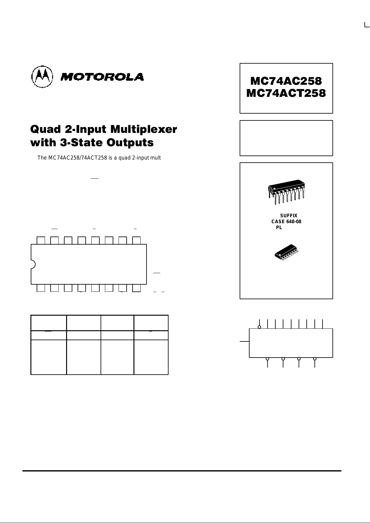
1516 14 13 12 11 10
21 3 4 5 6 7
V
CC
9
8
OE I0cI
1c
Z
cI0dI1dZd
S I
0aI1a
Z
aI0bI1bZb
GND
PIN NAMES
S Common Data Select Input
OE
3-State Output Enable Input
I0a–I0d Data Inputs from Source 0
I1a–I1d Data Inputs from Source 1
Za–Zd 3-State Multiplexer Outputs
TRUTH TABLE
Output
Enable
Select
Input
Data
Inputs
Outputs
OE S I
0
I
1
Z
H X X X Z
L H X L H
L H X H L
L L L X H
L L H X L
H = HIGH Voltage Level
L = LOW Voltage Level
X = Immaterial
Z = High Impedance
QUAD 2-INPUT
MULTIPLEXER WITH
3-STATE OUTPUTS
N SUFFIX
CASE 648-08
PLASTIC
D SUFFIX
CASE 751B-05
PLASTIC
LOGIC SYMBOL
S
OE I0aI1aI0bI
1b
Z
b
I0cI1cI0dI
1d
Z
a
Z
c
Z
d
MC74AC258 MC74ACT258
5-2
FACT DATA
FUNCTIONAL DESCRIPTION
The MC74AC258/74ACT258 is a quad 2-input multiplexer
with 3-state outputs. It selects four bits of data from two
sources under control of a common Select input (S). When the
Select input is LOW, the I0x inputs are selected and when
Select is HIGH, the I1x inputs are selected. The data on the
selected inputs appears at the outputs in inverted form. The
MC74AC258/74ACT258 is the logic implementation of a
4-pole, 2-position switch where the position of the switch is
determined by the logic levels supplied to the Select input. The
logic equations for the outputs are shown below:
Z
a
= OE
•(I1a•S+I0a•S)
Z
b
= OE
•(I1b•S+I0b•S)
Z
c
= OE
•(I1c•S+I0c•S)
Zd = OE
•(I1d•S+I0d•S)
When the Output Enable input (OE) is HIGH, the outputs
are forced to a high impedance state. If the outputs of the
3-state devices are tied together, all but one device must be in
the high impedance state to avoid high currents that would
exceed the maximum ratings. Designers should ensure the
Output Enable signals to 3-state devices whose outputs are
tied together are designed so there is no overlap.
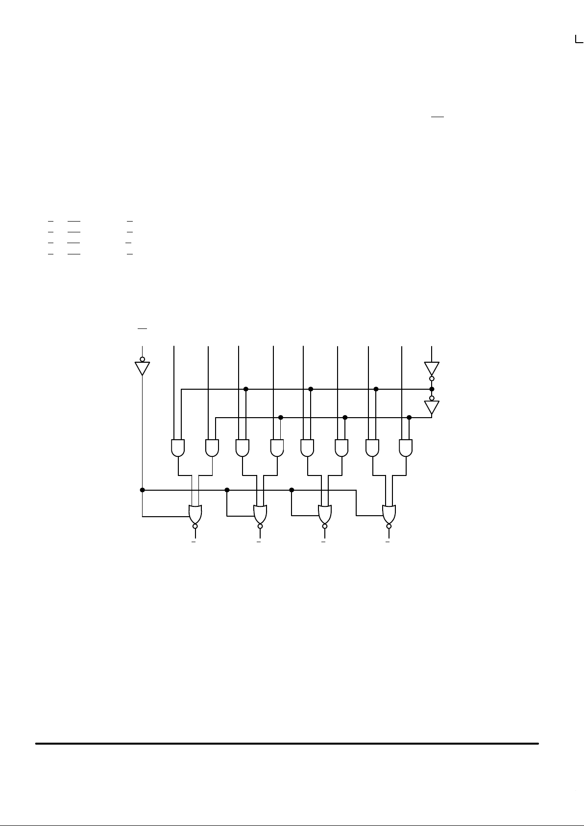
Please note that this diagram is provided only for the understanding of logic
operations and should not be used to estimate propagation delays.
OE I
0a
I
1a
I
0b
I
1b
I
0c
I
1c
I
0d
I
1d
S
Z
a
Z
b
Z
c
Z
d
LOGIC DIAGRAM

MC74AC258 MC74ACT258
5-3
FACT DATA
MAXIMUM RATINGS*
Symbol Parameter Value Unit
V
CC
DC Supply Voltage (Referenced to GND) –0.5 to +7.0 V
V
in
DC Input Voltage (Referenced to GND) –0.5 to VCC +0.5 V
V
out
DC Output Voltage (Referenced to GND) –0.5 to VCC +0.5 V
I
in
DC Input Current, per Pin ±20 mA
I
out
DC Output Sink/Source Current, per Pin ±50 mA
I
CC
DC VCC or GND Current per Output Pin ±50 mA
T
stg
Storage Temperature –65 to +150 °C
* Maximum Ratings are those values beyond which damage to the device may occur. Functional operation should be restricted to the Recommended
Operating Conditions.
RECOMMENDED OPERATING CONDITIONS
Symbol Parameter Min Typ Max Unit
′AC 2.0 5.0 6.0
VCCSupply Voltage
′ACT 4.5 5.0 5.5
V
Vin, V
out
DC Input Voltage, Output Voltage (Ref. to GND) 0 V
CC
V
VCC @ 3.0 V 150
tr, t
f
Input Rise and Fall Time (Note 1)
′AC Devices except Schmitt Inputs
VCC @ 4.5 V 40 ns/V
r
, t
f
′AC Devices except Schmitt Inputs
VCC @ 5.5 V 25
Input Rise and Fall Time (Note 2)
VCC @ 4.5 V 10
tr, t
f
Input Rise and Fall Time (Note 2)
′ACT Devices except Schmitt Inputs
VCC @ 5.5 V 8.0
ns/V
T
J
Junction Temperature (PDIP) 140 °C
T
A
Operating Ambient Temperature Range –40 25 85 °C
I
OH
Output Current — High –24 mA
I
OL
Output Current — Low 24 mA
1. Vin from 30% to 70% VCC; see individual Data Sheets for devices that differ from the typical input rise and fall times.
2. Vin from 0.8 V to 2.0 V; see individual Data Sheets for devices that differ from the typical input rise and fall times.
 Loading...