

5-1
FACT DATA
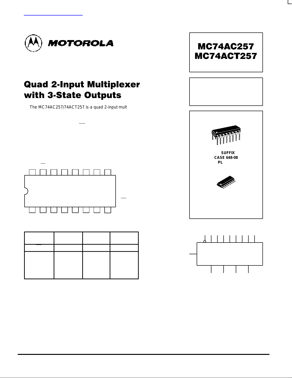
The MC74AC257/74ACT257 is a quad 2-input multiplexer with 3-state outputs.
Four bits of data from two sources can be selected using a Common Data Select
input. The four outputs present the selected data in true (noninverted) form. The
outputs may be switched to a high impedance state by placing a logic HIGH on
the common Output Enable (OE
) input, allowing the outputs to interface directly
with bus-oriented systems.
• Multiplexer Expansion by Tying Outputs Together
• Noninverting 3-State Outputs
• Outputs Source/Sink 24 mA
• ′ACT257 Has TTL Compatible Inputs
1516 14 13 12 11 10
21 3 4 5 6 7
V
CC
9
8
OE I
0cI1cZcI0dI1dZd
S I
0aI1aZaI0bI1bZb
GND
PIN NAMES
S Common Data Select Input
OE
3-State Output Enable Input
I0a–I
0d
Data Inputs from Source 0
I1a–I
1d
Data Inputs from Source 1
Za–Zd3-State Multiplexer Outputs
TRUTH TABLE
Output
Enable
Select
Input
Data
Inputs
Outputs
OE S I
0
I
1
Z
H X X X Z
L H X L L
L H X H H
L L L X L
L L H X H
H = HIGH Voltage Level
L = LOW Voltage Level
X = Immaterial
Z = High Impedance
QUAD 2-INPUT
MULTIPLEXER WITH
3-STATE OUTPUTS
N SUFFIX
CASE 648-08
PLASTIC
D SUFFIX
CASE 751B-05
PLASTIC
LOGIC SYMBOL
S
OE I0aI1aI0bI
1b
Z
b
I0cI1cI0dI
1d
Z
a
Z
c
Z
d
查询MC74AC257供应商
MC74AC257 MC74ACT257
5-2
FACT DATA
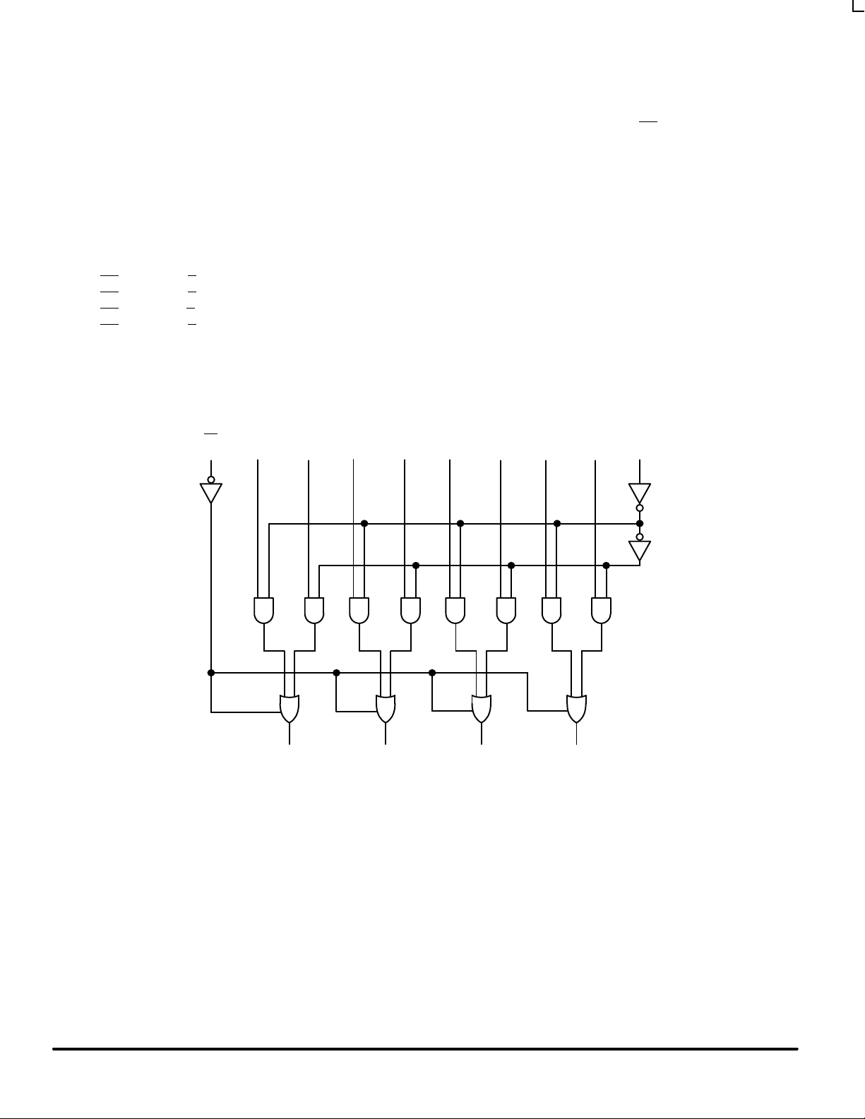
FUNCTIONAL DESCRIPTION
The MC74AC257/74ACT257 is a quad 2-input multiplexer
with 3-state outputs. It selects four bits of data from two
sources under control of a Common Data Select input. When
the Select input is LOW, the I0x inputs are selected and when
Select is HIGH, the I1x inputs are selected. The data on the
selected inputs appears at the outputs in true (noninverted)
form. The device is the logic implementation of a 4-pole,
2-position switch where the position of the switch is
determined by the logic levels supplied to the Select input. The
logic equations for the outputs are shown below:
Za = OE
•(I1a•S+I0a•S)
Zb = OE
•(I1b•S+I0b•S)
Zc = OE
•(I1c•S+I0c•S)
Zd = OE
•(I1d•S+I0d•S)
When the Output Enable input (OE) is HIGH, the outputs
are forced to a high impedance state. If the outputs are tied
together, all but one device must be in the high impedance
state to avoid high currents that would exceed the maximum
ratings. Designers should ensure the Output Enable signals to
3-state devices whose outputs are tied together are designed
so there is no overlap.
Please note that this diagram is provided only for the understanding of logic
operations and should not be used to estimate propagation delays.
OE I
0a
I
1a
I
0b
I
1b
I
0c
I
1c
I
0d
I
1d
S
Z
a
Z
b
Z
c
Z
d
LOGIC DIAGRAM
MC74AC257 MC74ACT257
5-3
FACT DATA
MAXIMUM RATINGS*
Symbol Parameter Value Unit
V
CC
DC Supply Voltage (Referenced to GND) –0.5 to +7.0 V
V
in
DC Input Voltage (Referenced to GND) –0.5 to VCC +0.5 V
V
out
DC Output Voltage (Referenced to GND) –0.5 to VCC +0.5 V
I
in
DC Input Current, per Pin ±20 mA
I
out
DC Output Sink/Source Current, per Pin ±50 mA
I
CC
DC VCC or GND Current per Output Pin ±50 mA
T
stg
Storage Temperature –65 to +150 °C
* Maximum Ratings are those values beyond which damage to the device may occur. Functional operation should be restricted to the Recommended
Operating Conditions.
RECOMMENDED OPERATING CONDITIONS
Symbol Parameter Min Typ Max Unit
′AC 2.0 5.0 6.0
VCCSupply Voltage
′ACT 4.5 5.0 5.5
V
Vin, V
out
DC Input Voltage, Output Voltage (Ref. to GND) 0 V
CC
V
VCC @ 3.0 V 150
Input Rise and Fall Time (Note 1)
′AC Devices except Schmitt Inputs
VCC @ 4.5 V 40 ns/V
r
, t
f
′AC Devices except Schmitt Inputs
VCC @ 5.5 V 25
VCC @ 4.5 V 10
tr, t
f
Input Rise and Fall Time (Note 2)
′ACT Devices except Schmitt Inputs
VCC @ 5.5 V 8.0
ns/V
T
J
Junction Temperature (PDIP) 140 °C
T
A
Operating Ambient Temperature Range –40 25 85 °C
I
OH
Output Current — High –24 mA
I
OL
Output Current — Low 24 mA
1. Vin from 30% to 70% VCC; see individual Data Sheets for devices that differ from the typical input rise and fall times.
2. Vin from 0.8 V to 2.0 V; see individual Data Sheets for devices that differ from the typical input rise and fall times.
tr, t
f
Input Rise and Fall Time (Note 2)

MC74AC257 MC74ACT257
5-4
FACT DATA
DC CHARACTERISTICS
74AC 74AC
Symbol
Parameter
V
CC
(V)
TA = +25°C
TA =
–40°C to +85°C
Unit
Conditions
Typ Guaranteed Limits
V
IH
3.0 1.5 2.1 2.1 V
OUT
= 0.1 V
4.5 2.25 3.15 3.15 V or VCC – 0.1 V
5.5 2.75 3.85 3.85
V
IL
3.0 1.5 0.9 0.9 V
OUT
= 0.1 V
4.5 2.25 1.35 1.35 V or VCC – 0.1 V
5.5 2.75 1.65 1.65
V
OH
3.0 2.99 2.9 2.9 I
OUT
= –50 µA
4.5 4.49 4.4 4.4 V
5.5 5.49 5.4 5.4
*VIN = VIL or V
IH
3.0 2.56 2.46
–12 mA
4.5 3.86 3.76
V
I
OH
–24 mA
5.5 4.86 4.76 –24 mA
V
OL
3.0 0.002 0.1 0.1 I
OUT
= 50 µA
4.5 0.001 0.1 0.1 V
5.5 0.001 0.1 0.1
*VIN = VIL or V
IH
3.0 0.36 0.44
12 mA
4.5 0.36 0.44
V
I
OL
24 mA
5.5 0.36 0.44 24 mA
I
IN
5.5
±0.1
±1.0
µA
VI = VCC, GND
I
OZ
VI (OE) = VIL, V
IH
5.5 ±0.5 ±5.0 µA VI = VCC, GND
VO = VCC, GND
I
OLD
5.5 75 mA V
OLD
= 1.65 V Max
I
OHD
Output Current
5.5 –75 mA V
OHD
= 3.85 V Min
I
CC
5.5
8.080µA
VIN = VCC or GND
* All outputs loaded; thresholds on input associated with output under test.
†Maximum test duration 2.0 ms, one output loaded at a time.
Note: IIN and ICC @ 3.0 V are guaranteed to be less than or equal to the respective limit @ 5.5 V VCC.
Minimum High Level
Input Voltage
Maximum Low Level
Input Voltage
Minimum High Level
Output Voltage
Maximum Low Level
Output Voltage
Maximum Input
Leakage Current
Maximum
3-State
Current
†Minimum Dynamic
Maximum Quiescent
Supply Current

MC74AC257 MC74ACT257
5-5
FACT DATA
AC CHARACTERISTICS (For Figures and Waveforms — See Section 3)
74AC 74AC
Symbol
Parameter
VCC*
(V)
TA = +25°C
CL = 50 pF
TA = –40°C
to +85°C
CL = 50 pF
Unit
Fig.
No.
Min Typ Max Min Max
Propagation Delay
3.3 1.5 5.0 8.5 1.0 9.0
t
PLH
In to Z
n
5.0 1.5 4.0 6.0 1.0 7.0
ns
3-5
Propagation Delay
3.3 1.5 6.0 8.5 1.0 9.0
t
PHL
In to Z
n
5.0 1.5 4.5 6.0 1.0 7.0
ns
3-5
Propagation Delay
3.3 1.5 7.0 10.5 1.5 11.5
t
PLH
S to Z
n
5.0 1.5 5.0 7.5 1.0 8.5
ns
3-6
Propagation Delay
3.3 1.5 7.5 10.5 1.5 11.5
t
PHL
S to Z
n
5.0 1.5 5.5 7.5 1.0 8.5
ns
3-6
3.3 1.5 6.5 9.5 1.0 10.5
t
PZH
Output Enable Time
5.0 1.5 5.0 7.5 1.0 8.5
ns
3-7
3.3 1.5 5.5 9.0 1.0 10.0
t
PZL
Output Enable Time
5.0 1.5 5.0 8.5 1.0 9.5
ns
3-8
3.3 1.5 5.5 10.0 1.0 11.0
t
PHZ
Output Disable Time
5.0 1.5 5.0 9.0 1.0 10.0
ns
3-7
3.3 1.5 5.5 9.0 1.0 10.0
t
PLZ
Output Disable Time
5.0 1.5 5.0 8.0 1.0 9.0
ns
3-8
* Voltage Range 3.3 V is 3.3 V ±0.3 V.
Voltage Range 5.0 V is 5.0 V ±0.5 V.

MC74AC257 MC74ACT257
5-6
FACT DATA
DC CHARACTERISTICS
74ACT 74ACT
Symbol
Parameter
V
CC
(V)
TA = +25°C
TA =
–40°C to +85°C
Unit
Conditions
Typ Guaranteed Limits
V
IH
4.5 1.5 2.0 2.0
V
OUT
= 0.1 V
5.5 1.5 2.0 2.0
V
or VCC – 0.1 V
V
IL
4.5 1.5 0.8 0.8
V
OUT
= 0.1 V
5.5 1.5 0.8 0.8
V
or VCC – 0.1 V
V
OH
4.5 4.49 4.4 4.4
I
OUT
= –50 µA
5.5 5.49 5.4 5.4
V
*VIN = VIL or V
IH
4.5 3.86 3.76 V
–24 mA
5.5 4.86 4.76
I
OH
–24 mA
V
OL
4.5 0.001 0.1 0.1
I
OUT
= 50 µA
5.5 0.001 0.1 0.1
V
*VIN = VIL or V
IH
4.5 0.36 0.44 V
24 mA
5.5 0.36 0.44
I
OL
24 mA
I
IN
5.5
±0.1
±1.0
µA
VI = VCC, GND
∆I
CCT
Additional Max. ICC/Input 5.5 0.6 1.5 mA VI = VCC – 2.1 V
I
OZ
VI (OE) = VIL, V
IH
5.5 ±0.5 ±5.0 µA VI = VCC, GND
VO = VCC, GND
I
OLD
5.5 75 mA V
OLD
= 1.65 V Max
I
OHD
Output Current
5.5 –75 mA V
OHD
= 3.85 V Min
I
CC
5.5
8.080µA
VIN = VCC or GND
* All outputs loaded; thresholds on input associated with output under test.
†Maximum test duration 2.0 ms, one output loaded at a time.
Minimum High Level
Input Voltage
Maximum Low Level
Input Voltage
Minimum High Level
Output Voltage
Maximum Low Level
Output Voltage
Maximum Input
Leakage Current
Maximum
3-State
Current
†Minimum Dynamic
Maximum Quiescent
Supply Current

MC74AC257 MC74ACT257
5-7
FACT DATA
AC CHARACTERISTICS (For Figures and Waveforms — See Section 3)
74ACT 74ACT
Symbol
Parameter
VCC*
(V)
TA = +25°C
CL = 50 pF
TA = –40°C
to +85°C
CL = 50 pF
Unit
Fig.
No.
Min Typ Max Min Max
t
PLH
5.0
1.5
5.0
7.0
1.0
7.5ns3-6
t
PHL
5.0
2.0
6.0
7.5
1.5
8.5ns3-6
t
PLH
5.0
2.0
7.0
9.5
1.5
10.5ns3-6
t
PHL
5.0
2.5
7.0
10.5
2.0
11.5ns3-6
t
PZH
Output Enable Time 5.0 2.0 6.0 8.0 1.5 9.0 ns 3-7
t
PZL
Output Enable Time 5.0 2.0 6.0 8.0 1.5 9.0 ns 3-8
t
PHZ
Output Disable Time 5.0 2.5 6.5 9.0 1.5 10.0 ns 3-7
t
PLZ
Output Disable Time 5.0 2.0 6.0 7.5 1.5 8.5 ns 3-8
* Voltage Range 5.0 V is 5.0 V ±0.5 V.
CAPACITANCE
Symbol Parameter
Value
Typ
Unit Test Conditions
C
IN
Input Capacitance 4.5 pF VCC = 5.0 V
C
PD
Power Dissipation Capacitance 50 pF VCC = 5.0 V
Propagation Delay
In to Z
n
Propagation Delay
In to Z
n
Propagation Delay
S to Z
n
Propagation Delay
S to Z
n
MC74AC257 MC74ACT257
5-8
FACT DATA
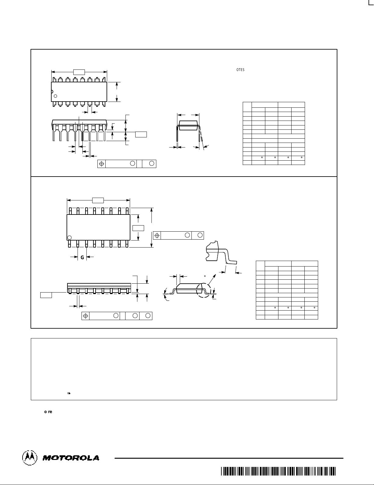
OUTLINE DIMENSIONS
N SUFFIX
PLASTIC DIP PACKAGE
CASE 648–08
ISSUE R
D SUFFIX
PLASTIC SOIC PACKAGE
CASE 751B–05
ISSUE J
NOTES:
1. DIMENSIONING AND TOLERANCING PER
ANSI Y14.5M, 1982.
2. CONTROLLING DIMENSION: MILLIMETER.
3. DIMENSIONS A AND B DO NOT INCLUDE
MOLD PROTRUSION.
4. MAXIMUM MOLD PROTRUSION 0.15 (0.006)
PER SIDE.
5. DIMENSION D DOES NOT INCLUDE DAMBAR
PROTRUSION. ALLOWABLE DAMBAR
PROTRUSION SHALL BE 0.127 (0.005) TOTAL
IN EXCESS OF THE D DIMENSION AT
MAXIMUM MATERIAL CONDITION.
1 8
16 9
SEATING
PLANE
F
J
M
R
X 45
_
G
8 PLP
–B–
–A–
M
0.25 (0.010) B
S
–T–
D
K
C
16 PL
S
B
M
0.25 (0.010) A
S
T
DIM MIN MAX MIN MAX
INCHESMILLIMETERS
A 9.80 10.00 0.386 0.393
B 3.80 4.00 0.150 0.157
C 1.35 1.75 0.054 0.068
D 0.35 0.49 0.014 0.019
F 0.40 1.25 0.016 0.049
G 1.27 BSC 0.050 BSC
J 0.19 0.25 0.008 0.009
K 0.10 0.25 0.004 0.009
M 0 7 0 7
P 5.80 6.20 0.229 0.244
R 0.25 0.50 0.010 0.019
_ _ _ _
NOTES:
1. DIMENSIONING AND TOLERANCING PER ANSI
Y14.5M, 1982.
2. CONTROLLING DIMENSION: INCH.
3. DIMENSION L TO CENTER OF LEADS WHEN
FORMED PARALLEL.
4. DIMENSION B DOES NOT INCLUDE MOLD FLASH.
5. ROUNDED CORNERS OPTIONAL.
–A–
B
F
C
S
H
G
D
J
L
M
16 PL
SEATING
1 8
916
K
PLANE
–T–
M
A
M
0.25 (0.010) T
DIM MIN MAX MIN MAX
MILLIMETERSINCHES
A 0.740 0.770 18.80 19.55
B 0.250 0.270 6.35 6.85
C 0.145 0.175 3.69 4.44
D 0.015 0.021 0.39 0.53
F 0.040 0.70 1.02 1.77
G 0.100 BSC 2.54 BSC
H 0.050 BSC 1.27 BSC
J 0.008 0.015 0.21 0.38
K 0.110 0.130 2.80 3.30
L 0.295 0.305 7.50 7.74
M 0 10 0 10
S 0.020 0.040 0.51 1.01
____
How to reach us:
USA/EUROPE: Motorola Literature Distribution; JAPAN: Nippon Motorola Ltd.; Tatsumi–SPD–JLDC, Toshikatsu Otsuki,
P.O. Box 20912; Phoenix, Arizona 85036. 1–800–441–2447 6F Seibu–Butsuryu–Center, 3–14–2 Tatsumi Koto–Ku, Tokyo 135, Japan. 03–3521–8315
MFAX: RMFAX0@email.sps.mot.com –TOUCHTONE (602) 244–6609 HONG KONG: Motorola Semiconductors H.K. Ltd.; 8B Tai Ping Industrial Park,
INTERNET: http://Design–NET.com 51 Ting Kok Road, Tai Po, N.T., Hong Kong. 852–26629298
Motorola reserves the right to make changes without further notice to any products herein. Motorola makes no warranty , representation or guarantee regarding
the suitability of its products for any particular purpose, nor does Motorola assume any liability arising out of the application or use of any product or circuit, and
specifically disclaims any and all liability , including without limitation consequential or incidental damages. “Typical” parameters can and do vary in different
applications. All operating parameters, including “T ypicals” must be validated for each customer application by customer’s technical experts. Motorola does
not convey any license under its patent rights nor the rights of others. Motorola products are not designed, intended, or authorized for use as components in
systems intended for surgical implant into the body, or other applications intended to support or sustain life, or for any other application in which the failure of
the Motorola product could create a situation where personal injury or death may occur. Should Buyer purchase or use Motorola products for any such
unintended or unauthorized application, Buyer shall indemnify and hold Motorola and its officers, employees, subsidiaries, affiliates, and distributors harmless
against all claims, costs, damages, and expenses, and reasonable attorney fees arising out of, directly or indirectly, any claim of personal injury or death
associated with such unintended or unauthorized use, even if such claim alleges that Motorola was negligent regarding the design or manufacture of the part.
Motorola and are registered trademarks of Motorola, Inc. Motorola, Inc. is an Equal Opportunity/Affirmative Action Employer.
MC74AC257/D
*MC74AC257/D*
◊
 Loading...