

Motorola MC74ACT256D, MC74ACT256N, MC74AC256D, MC74AC256N Datasheet
5-1
FACT DATA
The MC74AC256/74ACT256 dual addressable latch has four distinct modes
of operation which are selectable by controlling the Clear and Enable inputs
(see Function Table). In the addressable latch mode, data at the Data (D) inputs
is written into the addressed latches. The addressed latches will follow the Data
input with all unaddressed latches remaining in their previous states.
In the memory mode, all latches remain in their previous states and are
unaffected by the Data or Address inputs. To eliminate the possibility of entering
erroneous data in the latches, the enable should be held HIGH (inactive) while
the address lines are changing. In the dual 1-of-4 decoding or demultiplexing
mode (MR
= E = LOW), addressed outputs will follow the level of the D inputs
with all other outputs LOW. In the clear mode, all outputs are LOW and unaffected
by the Address and Data inputs.
• Combines Dual Demultiplexer and 8-Bit Latch
• Serial-to-Parallel Capability
• Output from Each Storage Bit Available
• Random (Addressable) Data Entry
• Easily Expandable
• Common Clear Input
• Useful as Dual 1-of-4 Active HIGH Decoder
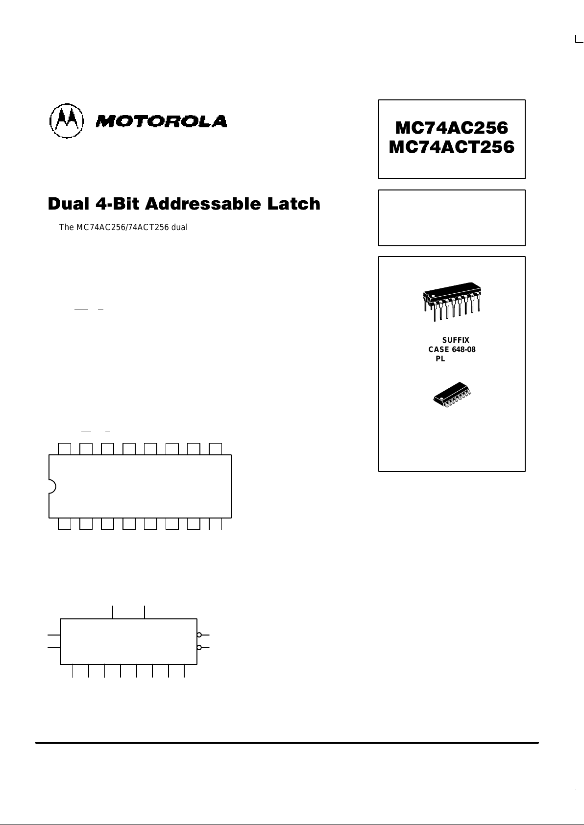
1516 14 13 12 11 10
21 3 4 5 6 7
V
CC
9
8
MR E DbQ3bQ2bQ1bQ
0b
A0A1DaQ0aQ1aQ2aQ3aGND
DUAL 4-BIT
ADDRESSABLE
LATCH
N SUFFIX
CASE 648-08
PLASTIC
D SUFFIX
CASE 751B-05
PLASTIC
LOGIC SYMBOL
D
a
D
b
A
0
A
1
E
MR
Q0aQ1aQ2aQ3aQ0bQ1bQ2bQ
3b
MC74AC256 MC74ACT256
5-2
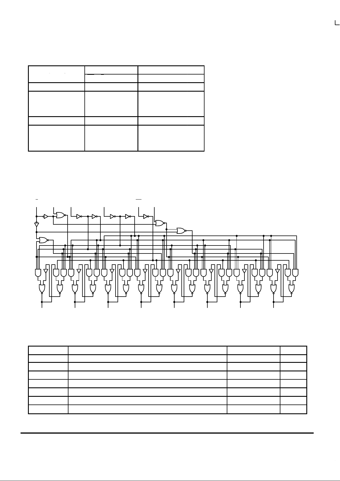
FACT DATA
MODE SELECT-FUNCTION TABLE
Operating
Inputs Outputs
Operating
Mode
MR E D A0A1Q
0
Q
1
Q
2
Q
3
Master Reset L H X X X L L L L
L L d L L Q = d L L L
Demultiplex (Active HIGH L L d H L L Q = d L L
Decoder when D = H) L L d L H L L Q = d L
L L d H H L L L Q = d
Store (Do Nothing) H H X X X q
0
q
1
q
2
q
3
H L d L L Q = d q
1
q
2
q
3
Addressable H L d H L q0Q = d q
2
q
3
Latch H L d L H q
0
q1Q = d q
3
H L d H H q
0
q
1
q2Q = d
H = HIGH Voltage Level Steady State
L = LOW Voltage Level Steady State
X = Immaterial
d = HIGH or LOW Data one setup time prior to the LOW-to-HIGH Enable transition
q = Lower case letters indicate the state of the referenced output established during the last cycle in
which it was addressed or cleared.
D
a
A
0
A
1
MR D
b
Q
1a
Q
2a
Q
3a
Q
0b
Q
1b
Q
2b
Q
3b
E
Q
0a
LOGIC DIAGRAM
Please note that this diagram is provided only for the understanding of logic
operations and should not be used to estimate propagation delays.
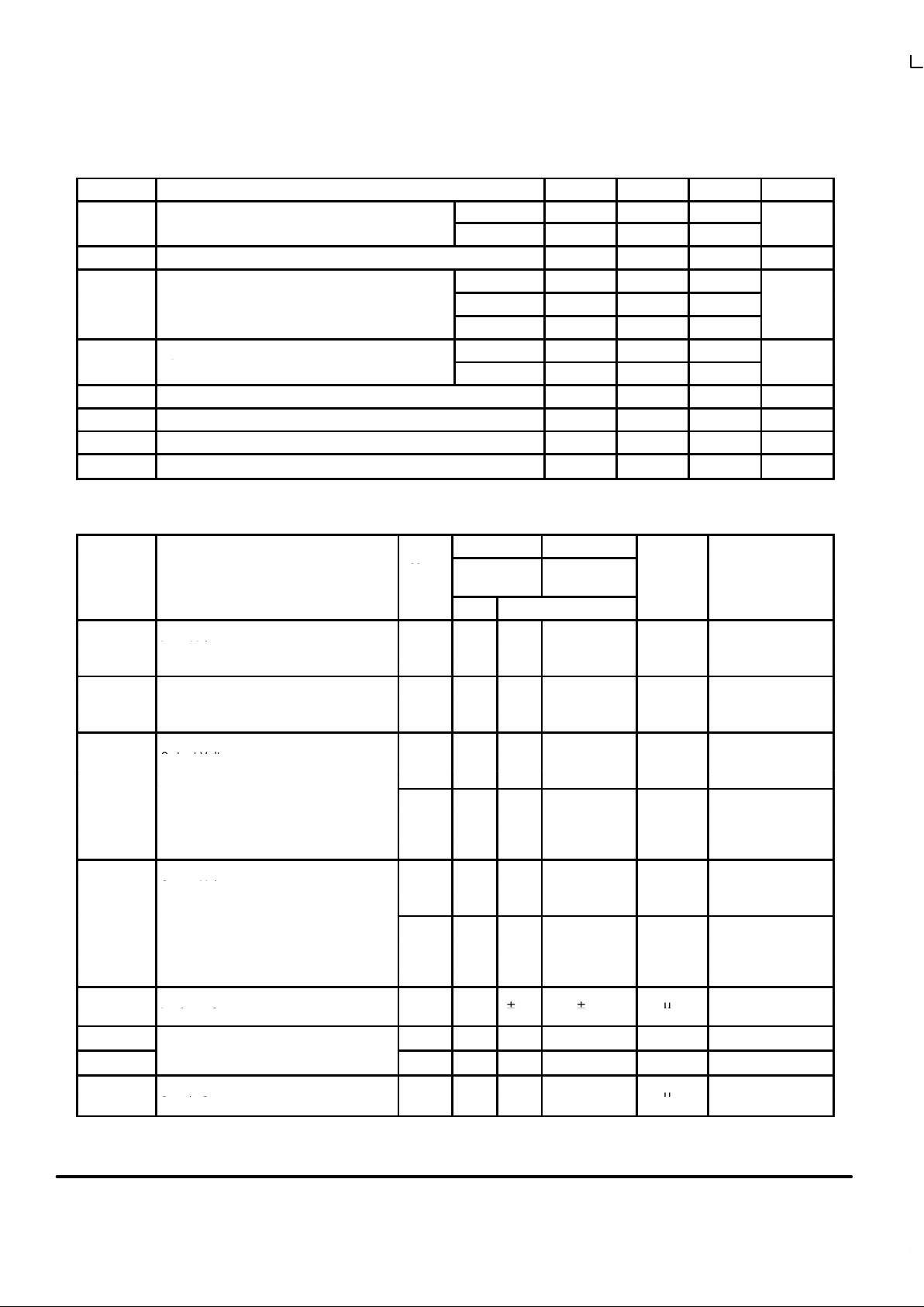
MAXIMUM RATINGS*
Symbol Parameter Value Unit
V
CC
DC Supply Voltage (Referenced to GND) –0.5 to +7.0 V
V
in
DC Input Voltage (Referenced to GND) –0.5 to VCC +0.5 V
V
out
DC Output Voltage (Referenced to GND) –0.5 to VCC +0.5 V
I
in
DC Input Current, per Pin ±20 mA
I
out
DC Output Sink/Source Current, per Pin ±50 mA
I
CC
DC VCC or GND Current per Output Pin ±50 mA
T
stg
Storage Temperature –65 to +150 °C
* Maximum Ratings are those values beyond which damage to the device may occur. Functional operation should be restricted to the Recommended
Operating Conditions.
MC74AC256 MC74ACT256
5-3
FACT DATA
RECOMMENDED OPERATING CONDITIONS
Symbol Parameter Min Typ Max Unit
′AC 2.0 5.0 6.0
VCCSupply Voltage
′ACT 4.5 5.0 5.5
V
Vin, V
out
DC Input Voltage, Output Voltage (Ref. to GND) 0 V
CC
V
VCC @ 3.0 V 150
tr, t
f
Input Rise and Fall Time (Note 1)
′AC Devices except Schmitt Inputs
VCC @ 4.5 V 40 ns/V
r
, t
f
′AC Devices except Schmitt Inputs
VCC @ 5.5 V 25
Input Rise and Fall Time (Note 2)
VCC @ 4.5 V 10
tr, t
f
Input Rise and Fall Time (Note 2)
′ACT Devices except Schmitt Inputs
VCC @ 5.5 V 8.0
ns/V
T
J
Junction Temperature (PDIP) 140 °C
T
A
Operating Ambient Temperature Range –40 25 85 °C
I
OH
Output Current — High –24 mA
I
OL
Output Current — Low 24 mA
1. Vin from 30% to 70% VCC; see individual Data Sheets for devices that differ from the typical input rise and fall times.
2. Vin from 0.8 V to 2.0 V; see individual Data Sheets for devices that differ from the typical input rise and fall times.
DC CHARACTERISTICS
74AC 74AC
Symbol
Parameter
V
CC
(V)
TA = +25°C
TA =
–40°C to +85°C
Unit
Conditions
Typ Guaranteed Limits
V
IH
Minimum High Level
3.0 1.5 2.1 2.1 V
OUT
= 0.1 V
Input Voltage
4.5 2.25 3.15 3.15 V or VCC – 0.1 V
5.5 2.75 3.85 3.85
V
IL
Maximum Low Level
3.0 1.5 0.9 0.9 V
OUT
= 0.1 V
Input Voltage
4.5 2.25 1.35 1.35 V or VCC – 0.1 V
5.5 2.75 1.65 1.65
V
OH
Minimum High Level
3.0 2.99 2.9 2.9 I
OUT
= –50 µA
Output Voltage
4.5 4.49 4.4 4.4 V
5.5 5.49 5.4 5.4
*VIN = VIL or V
IH
3.0 2.56 2.46
–12 mA
4.5 3.86 3.76
V
I
OH
–24 mA
5.5 4.86 4.76 –24 mA
V
OL
Maximum Low Level
3.0 0.002 0.1 0.1 I
OUT
= 50 µA
Output Voltage
4.5 0.001 0.1 0.1 V
5.5 0.001 0.1 0.1
*VIN = VIL or V
IH
3.0 0.36 0.44
12 mA
4.5 0.36 0.44
V
I
OL
24 mA
5.5 0.36 0.44 24 mA
I
IN
Maximum Input
Leakage Current
5.5
±0.1
±1.0
µA
VI = VCC, GND
I
OLD
†Minimum Dynamic
5.5 75 mA V
OLD
= 1.65 V Max
I
OHD
Output Current
5.5 –75 mA V
OHD
= 3.85 V Min
I
CC
Maximum Quiescent
Supply Current
5.5
8.080µA
VIN = VCC or GND
* All outputs loaded; thresholds on input associated with output under test.
†Maximum test duration 2.0 ms, one output loaded at a time.
Note: IIN and ICC @ 3.0 V are guaranteed to be less than or equal to the respective limit @ 5.5 V VCC.
 Loading...