

MOTOROLA MC74ACT174DTEL, MC74ACT174M, MC74ACT174MEL, MC74ACT174DR2, MC74ACT174DT Datasheet
...
5-1
FACT DATA
The MC74AC174/74ACT174 is a high-speed hex D flip-flop. The device is
used primarily as a 6-bit edge-triggered storage register. The information on the
D inputs is transferred to storage during the LOW-to-HIGH clock transition. The
device has a Master Reset to simultaneously clear all flip-flops.
• Outputs Source/Sink 24 mA
• ′ACT174 Has TTL Compatible Inputs
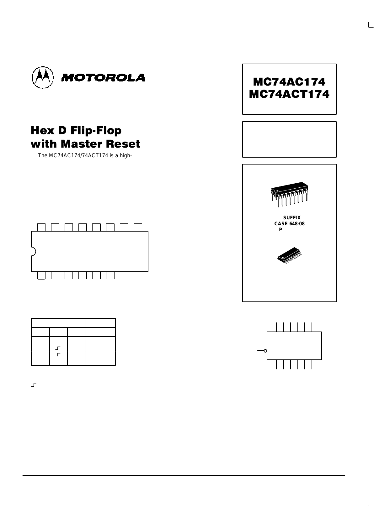
1516 14 13 12 11 10
21 3 4 5 6 7
V
CC
9
8
Q5D5D4Q4D3Q3CP
MR
Q0D0D1Q1D2Q2GND
PIN NAMES
D0–D5Data Inputs
CP Clock Pulse Input
MR
Master Reset Input
Q0–Q5Outputs
TRUTH TABLE
Inputs Output
MR CP D Q
L X X L
H H H
H L L
H L X Q
H = HIGH Voltage Level
L = LOW Voltage Level
X = Immaterial
= LOW-to-HIGH Transition of Clock
HEX D FLIP-FLOP
WITH MASTER RESET
N SUFFIX
CASE 648-08
PLASTIC
D SUFFIX
CASE 751B-05
PLASTIC
LOGIC SYMBOL
CP
MR
Q2Q3Q4Q
5
D0D1D2D3D4D
5
Q1Q
0
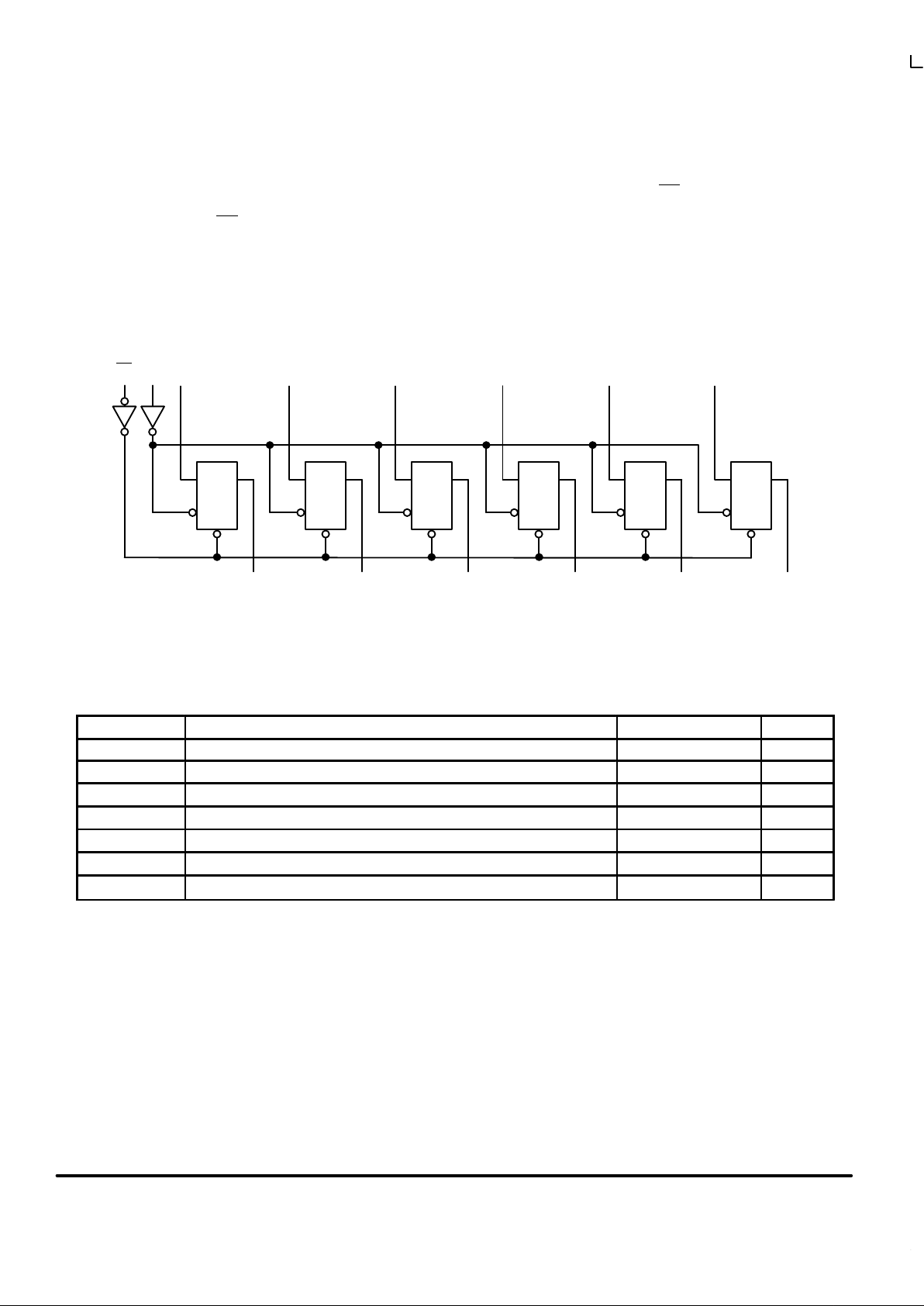
MC74AC174 MC74ACT174
5-2
FACT DATA
FUNCTIONAL DESCRIPTION
The M C74AC174/74ACT174 c onsists of six edge-triggered D
flip-flops with individual D inputs and Q outputs. The Clock
(CP) and Master Reset (MR
) are common to all flip-flops. Each
D input’s state is transferred to the corresponding flip-flop’s
output following the LOW-to-HIGH Clock (CP) transition. A
LOW input to the Master Reset (MR
) will force all outputs LOW
independent of Clock or Data inputs. The MC74AC174/
74ACT174 is useful for applications where the true output only
is required and the Clock and Master Reset are common to all
storage elements.
LOGIC DIAGRAM
CPMR
Q
5
D
5
Q
CD
Please note that this diagram is provided only for the understanding of logic
operations and should not be used to estimate propagation delays.
CP
D
Q
4
D
4
Q
CD
CP
D
Q
3
D
3
Q
CD
CP
D
Q
2
D
2
Q
CD
CP
D
Q
1
D
1
Q
CD
CP
D
Q
0
D
0
Q
CD
CP
D
MAXIMUM RATINGS*
Symbol Parameter Value Unit
V
CC
DC Supply Voltage (Referenced to GND) –0.5 to +7.0 V
V
in
DC Input Voltage (Referenced to GND) –0.5 to VCC +0.5 V
V
out
DC Output Voltage (Referenced to GND) –0.5 to VCC +0.5 V
I
in
DC Input Current, per Pin ±20 mA
I
out
DC Output Sink/Source Current, per Pin ±50 mA
I
CC
DC VCC or GND Current per Output Pin ±50 mA
T
stg
Storage Temperature –65 to +150 °C
* Maximum Ratings are those values beyond which damage to the device may occur. Functional operation should be restricted to the Recommended
Operating Conditions.
MC74AC174 MC74ACT174
5-3
FACT DATA
RECOMMENDED OPERATING CONDITIONS
Symbol Parameter Min Typ Max Unit
′AC 2.0 5.0 6.0
VCCSupply Voltage
′ACT 4.5 5.0 5.5
V
Vin, V
out
DC Input Voltage, Output Voltage (Ref. to GND) 0 V
CC
V
VCC @ 3.0 V 150
tr, t
f
Input Rise and Fall Time (Note 1)
′AC Devices except Schmitt Inputs
VCC @ 4.5 V 40 ns/V
r
, t
f
′AC Devices except Schmitt Inputs
VCC @ 5.5 V 25
Input Rise and Fall Time (Note 2)
VCC @ 4.5 V 10
tr, t
f
Input Rise and Fall Time (Note 2)
′ACT Devices except Schmitt Inputs
VCC @ 5.5 V 8.0
ns/V
T
J
Junction Temperature (PDIP) 140 °C
T
A
Operating Ambient Temperature Range –40 25 85 °C
I
OH
Output Current — High –24 mA
I
OL
Output Current — Low 24 mA
1. Vin from 30% to 70% VCC; see individual Data Sheets for devices that differ from the typical input rise and fall times.
2. Vin from 0.8 V to 2.0 V; see individual Data Sheets for devices that differ from the typical input rise and fall times.
DC CHARACTERISTICS
74AC 74AC
Symbol
Parameter
V
CC
(V)
TA = +25°C
TA =
–40°C to +85°C
Unit
Conditions
Typ Guaranteed Limits
V
IH
Minimum High Level
3.0 1.5 2.1 2.1 V
OUT
= 0.1 V
Input Voltage
4.5 2.25 3.15 3.15 V or VCC – 0.1 V
5.5 2.75 3.85 3.85
V
IL
Maximum Low Level
3.0 1.5 0.9 0.9 V
OUT
= 0.1 V
Input Voltage
4.5 2.25 1.35 1.35 V or VCC – 0.1 V
5.5 2.75 1.65 1.65
V
OH
Minimum High Level
3.0 2.99 2.9 2.9 I
OUT
= –50 µA
Output Voltage
4.5 4.49 4.4 4.4 V
5.5 5.49 5.4 5.4
*VIN = VIL or V
IH
3.0 2.56 2.46
–12 mA
4.5 3.86 3.76
V
I
OH
–24 mA
5.5 4.86 4.76 –24 mA
V
OL
Maximum Low Level
3.0 0.002 0.1 0.1 I
OUT
= 50 µA
Output Voltage
4.5 0.001 0.1 0.1 V
5.5 0.001 0.1 0.1
*VIN = VIL or V
IH
3.0 0.36 0.44
12 mA
4.5 0.36 0.44
V
I
OL
24 mA
5.5 0.36 0.44 24 mA
I
IN
Maximum Input
Leakage Current
5.5
±0.1
±1.0
µA
VI = VCC, GND
I
OLD
†Minimum Dynamic
5.5 75 mA V
OLD
= 1.65 V Max
I
OHD
Output Current
5.5 –75 mA V
OHD
= 3.85 V Min
I
CC
Maximum Quiescent
Supply Current
5.5
8.080µA
VIN = VCC or GND
* All outputs loaded; thresholds on input associated with output under test.
†Maximum test duration 2.0 ms, one output loaded at a time.
Note: IIN and ICC @ 3.0 V are guaranteed to be less than or equal to the respective limit @ 5.5 V VCC.
 Loading...