

Motorola MC74ACT174N, MC74ACT174D, MC74AC174D, MC74AC174N Datasheet
5-1
FACT DATA
The MC74AC174/74ACT174 is a high-speed hex D flip-flop. The device is
used primarily as a 6-bit edge-triggered storage register. The information on the
D inputs is transferred to storage during the LOW-to-HIGH clock transition. The
device has a Master Reset to simultaneously clear all flip-flops.
• Outputs Source/Sink 24 mA
• ′ACT174 Has TTL Compatible Inputs
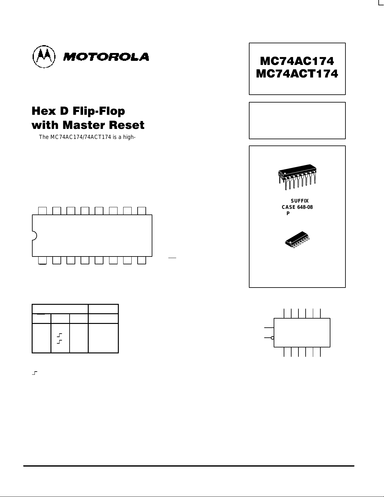
1516 14 13 12 11 10
21 3 4 5 6 7
V
CC
9
8
Q5D5D4Q4D3Q3CP
MR
Q0D0D1Q1D2Q2GND
PIN NAMES
D0–D5Data Inputs
CP Clock Pulse Input
MR
Master Reset Input
Q0–Q5Outputs
TRUTH TABLE
Inputs Output
MR CP D Q
L X X L
H H H
H L L
H L X Q
H = HIGH Voltage Level
L = LOW Voltage Level
X = Immaterial
= LOW-to-HIGH Transition of Clock
HEX D FLIP-FLOP
WITH MASTER RESET
N SUFFIX
CASE 648-08
PLASTIC
D SUFFIX
CASE 751B-05
PLASTIC
LOGIC SYMBOL
CP
MR
Q2Q3Q4Q
5
D0D1D2D3D4D
5
Q1Q
0
MC74AC174 MC74ACT174
5-2
FACT DATA
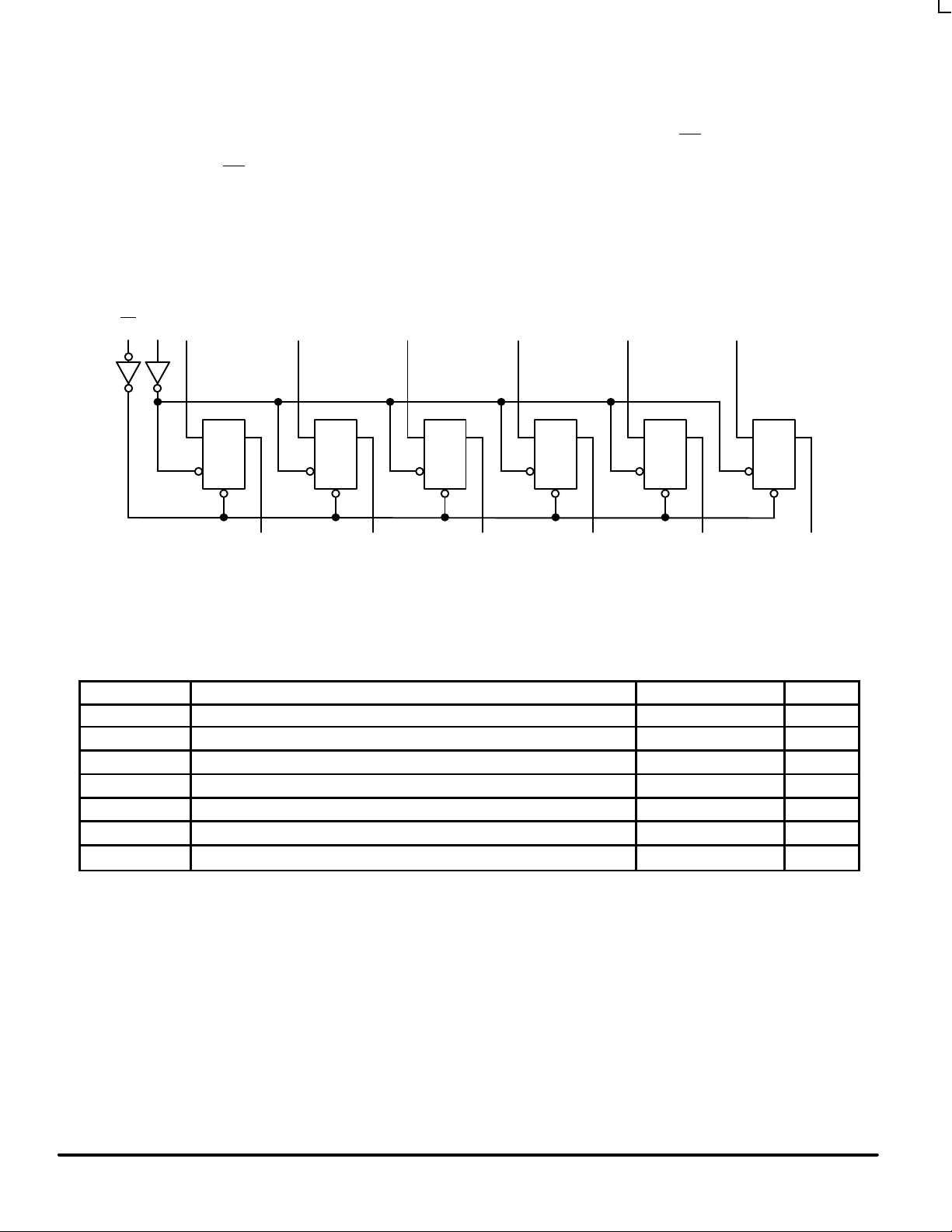
FUNCTIONAL DESCRIPTION
The M C74AC174/74ACT174 c onsists of s ix edge-triggered D
flip-flops with individual D inputs and Q outputs. The Clock
(CP) and Master Reset (MR
) are common to all flip-flops. Each
D input’s state is transferred to the corresponding flip-flop’s
output following the LOW-to-HIGH Clock (CP) transition. A
LOW input to the Master Reset (MR
) will force all outputs LOW
independent of Clock or Data inputs. The MC74AC174/
74ACT174 is useful for applications where the true output only
is required and the Clock and Master Reset are common to all
storage elements.
LOGIC DIAGRAM
CPMR
Q
5
D
5
Q
CD
Please note that this diagram is provided only for the understanding of logic
operations and should not be used to estimate propagation delays.
CP
D
Q
4
D
4
Q
CD
CP
D
Q
3
D
3
Q
CD
CP
D
Q
2
D
2
Q
CD
CP
D
Q
1
D
1
Q
CD
CP
D
Q
0
D
0
Q
CD
CP
D
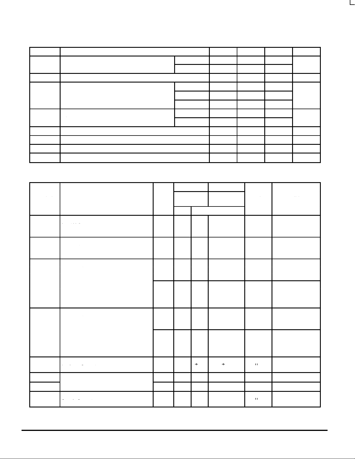
MAXIMUM RATINGS*
Symbol Parameter Value Unit
V
CC
DC Supply Voltage (Referenced to GND) –0.5 to +7.0 V
V
in
DC Input Voltage (Referenced to GND) –0.5 to VCC +0.5 V
V
out
DC Output Voltage (Referenced to GND) –0.5 to VCC +0.5 V
I
in
DC Input Current, per Pin ±20 mA
I
out
DC Output Sink/Source Current, per Pin ±50 mA
I
CC
DC VCC or GND Current per Output Pin ±50 mA
T
stg
Storage Temperature –65 to +150 °C
* Maximum Ratings are those values beyond which damage to the device may occur. Functional operation should be restricted to the Recommended
Operating Conditions.
MC74AC174 MC74ACT174
5-3
FACT DATA
RECOMMENDED OPERATING CONDITIONS
Symbol Parameter Min Typ Max Unit
′AC 2.0 5.0 6.0
VCCSupply Voltage
′ACT 4.5 5.0 5.5
V
Vin, V
out
DC Input Voltage, Output Voltage (Ref. to GND) 0 V
CC
V
VCC @ 3.0 V 150
Input Rise and Fall Time (Note 1)
′AC Devices except Schmitt Inputs
VCC @ 4.5 V 40 ns/V
r
, t
f
′AC Devices except Schmitt Inputs
VCC @ 5.5 V 25
VCC @ 4.5 V 10
tr, t
f
Input Rise and Fall Time (Note 2)
′ACT Devices except Schmitt Inputs
VCC @ 5.5 V 8.0
ns/V
T
J
Junction Temperature (PDIP) 140 °C
T
A
Operating Ambient Temperature Range –40 25 85 °C
I
OH
Output Current — High –24 mA
I
OL
Output Current — Low 24 mA
1. Vin from 30% to 70% VCC; see individual Data Sheets for devices that differ from the typical input rise and fall times.
2. Vin from 0.8 V to 2.0 V; see individual Data Sheets for devices that differ from the typical input rise and fall times.
DC CHARACTERISTICS
74AC 74AC
Symbol
Parameter
V
CC
(V)
TA = +25°C
TA =
–40°C to +85°C
Unit
Conditions
Typ Guaranteed Limits
V
IH
3.0 1.5 2.1 2.1 V
OUT
= 0.1 V
4.5 2.25 3.15 3.15 V or VCC – 0.1 V
5.5 2.75 3.85 3.85
V
IL
3.0 1.5 0.9 0.9 V
OUT
= 0.1 V
4.5 2.25 1.35 1.35 V or VCC – 0.1 V
5.5 2.75 1.65 1.65
V
OH
3.0 2.99 2.9 2.9 I
OUT
= –50 µA
4.5 4.49 4.4 4.4 V
5.5 5.49 5.4 5.4
*VIN = VIL or V
IH
3.0 2.56 2.46
–12 mA
4.5 3.86 3.76
V
I
OH
–24 mA
5.5 4.86 4.76 –24 mA
V
OL
3.0 0.002 0.1 0.1 I
OUT
= 50 µA
4.5 0.001 0.1 0.1 V
5.5 0.001 0.1 0.1
*VIN = VIL or V
IH
3.0 0.36 0.44
12 mA
4.5 0.36 0.44
V
I
OL
24 mA
5.5 0.36 0.44 24 mA
I
IN
5.5
±0.1
±1.0
µA
VI = VCC, GND
I
OLD
5.5 75 mA V
OLD
= 1.65 V Max
I
OHD
Output Current
5.5 –75 mA V
OHD
= 3.85 V Min
I
CC
5.5
8.080µA
VIN = VCC or GND
* All outputs loaded; thresholds on input associated with output under test.
†Maximum test duration 2.0 ms, one output loaded at a time.
Note: IIN and ICC @ 3.0 V are guaranteed to be less than or equal to the respective limit @ 5.5 V VCC.
tr, t
f
Input Rise and Fall Time (Note 2)
Minimum High Level
Input Voltage
Maximum Low Level
Input Voltage
Minimum High Level
Output Voltage
Maximum Low Level
Output Voltage
Maximum Input
Leakage Current
†Minimum Dynamic
Maximum Quiescent
Supply Current
 Loading...