

5-1
FACT DATA
The MC74AC160/74ACT160 and MC74AC162/74ACT162 are high-speed
synchronous decade counters operating in the BCD (8421) sequence. They
are synchronously presettable for application in programmable dividers and have
two types of Count Enable inputs plus a Terminal Count output for versatility in
forming synchronous multistage counters. The MC74AC160/74ACT160 has an
asynchronous Master Reset input that overrides all other inputs and forces the
outputs LOW. The MC74AC162/74ACT162 has a Synchronous Reset input that
overrides counting and parallel loading and allows all outputs to be simultaneously
reset on the rising edge of the clock.
• Synchronous Counting and Loading
• High-Speed Synchronous Expansion
• Typical Count Rate of 120 MHz
• Outputs Source/Sink 24 mA
• ′ACT160 and ′ACT162 Have TTL Compatible Inputs
1516 14 13 12 11 10
21 3 4 5 6 7
V
CC
9
8
*R
P
0
CP P1P2P3CEP GND
TC Q0Q1Q2Q3CET PE
PIN NAMES
CEP Count Enable Parallel Input
CET Count Enable Trickle Input
CP Clock Pulse Input
MR
(′160) Asynchronous Master Reset Input
SR
(′162) Synchronous Reset Input
P0–P3Parallel Data Inputs
PE
Parallel Enable Input
Q0–Q3Flip-Flop Outputs
TC Terminal Count Output
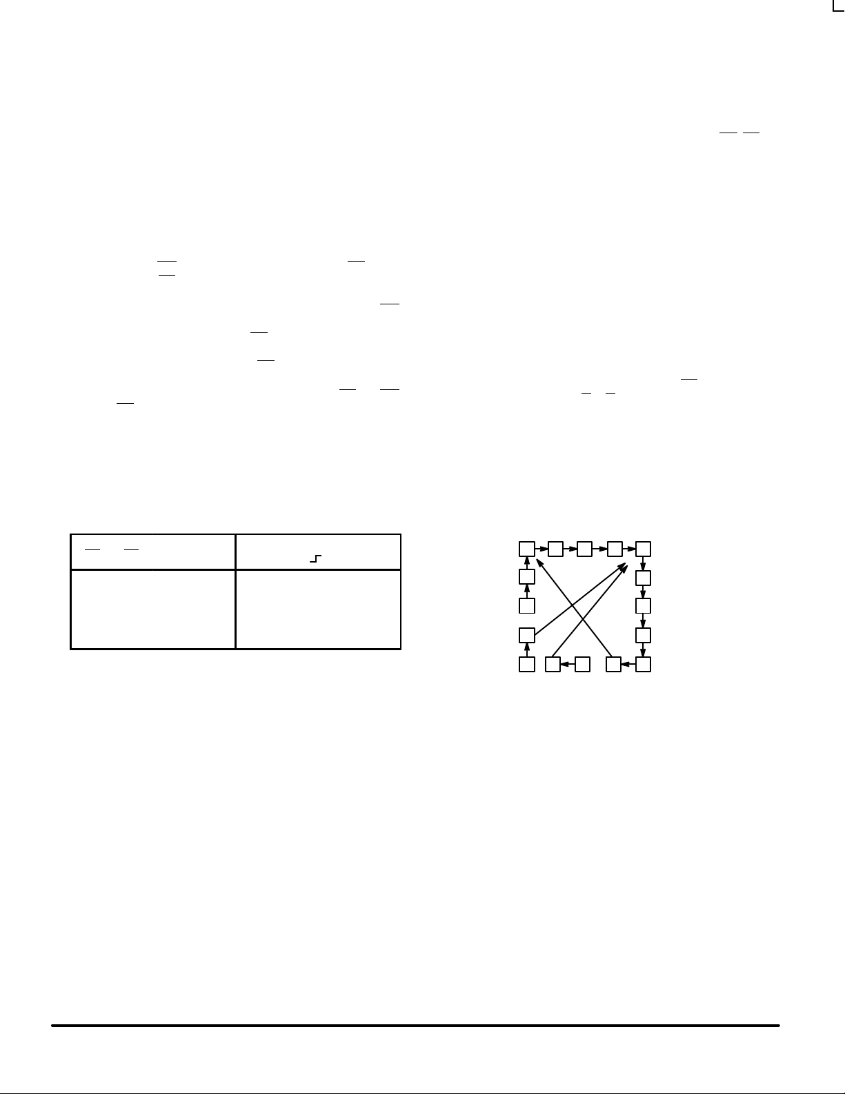
SYNCHRONOUS
PRESETTABLE
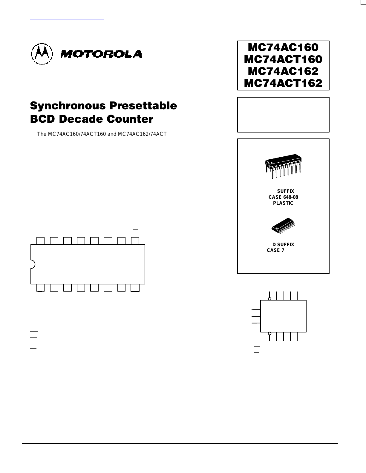
BCD DECADE COUNTER
N SUFFIX
CASE 648-08
PLASTIC
D SUFFIX
CASE 751B-05
PLASTIC
LOGIC SYMBOL
PE P0P1P
2
CEP
P
3
CET
CP
*R Q0Q1Q2Q
3
TC
*MR for ′160
*SR
for ′162
查询MC74AC160供应商
MC74AC160 MC74ACT160 MC74AC162 MC74ACT162
5-2
FACT DATA
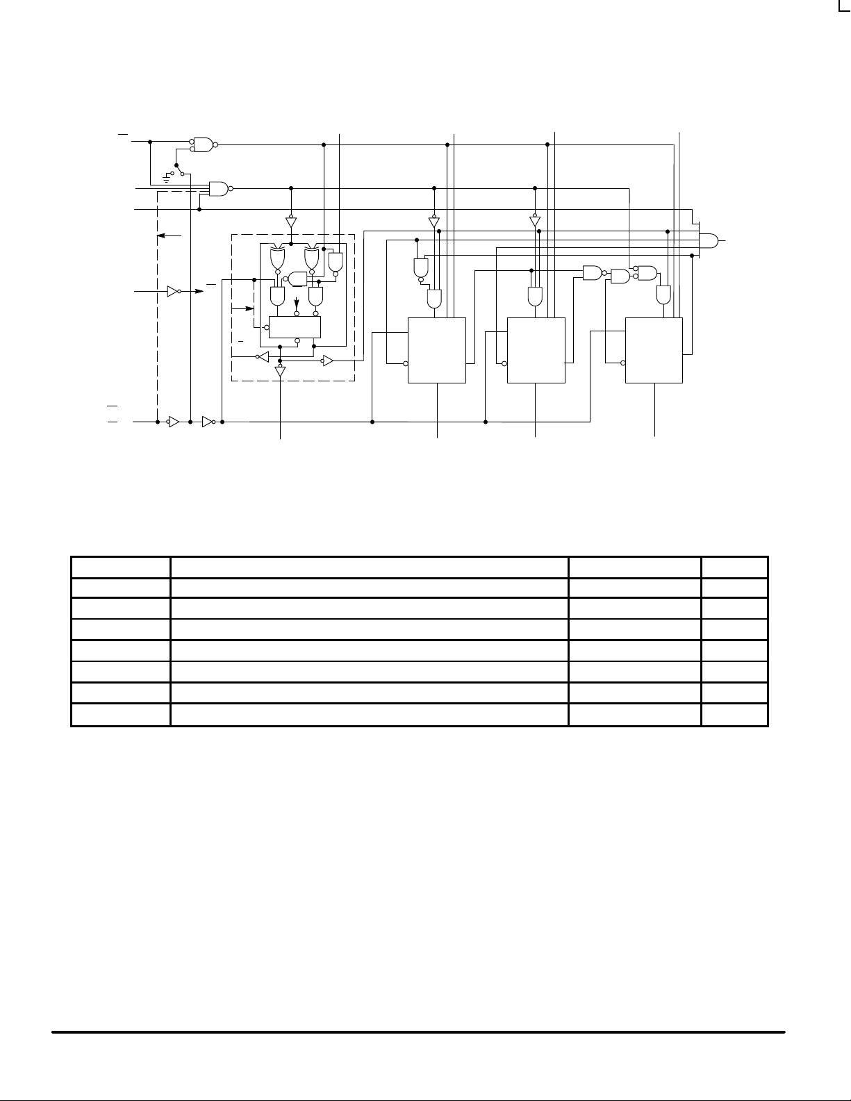
FUNCTIONAL DESCRIPTION
The MC74AC160/74ACT160 and MC74AC162/74ACT162
count modulo-10 in the BCD (8421) sequence. From state 9
(HLLH) they increment to state 0 (LLLL). The clock inputs of
all flip-flops are driven in parallel through a clock buffer. Thus
all changes of the Q outputs (except due to Master Reset of the
′160) occur as a result of, and synchronous with, the
LOW-to-HIGH transition of the CP input signal. The circuits
have four fundamental modes of operation, in order of
precedence: asynchronous reset (′160), synchronous reset
(′162), parallel load, count-up and hold. Five control inputs —
Master Reset (MR
, ′160), Synchronous Reset (SR,′162),
Parallel Enable (PE
), Count Enable Parallel (CEP) and Count
Enable Trickle (CET) — determine the mode of operation, as
shown in the Mode Select Table. A LOW signal on MR
overrides all other inputs and asynchronously forces all
outputs LOW. A LOW signal on SR
overrides counting and
parallel loading and allows all outputs to go LOW on the next
rising edge of CP . A LOW signal on PE
overrides counting and
allows information on the Parallel Data (Pn) inputs to be loaded
into the flip-flops on the next rising edge of CP . With PE
and MR
(′160) or SR (′162) HIGH, CEP and CET permit counting when
both are HIGH. Conversely, a LOW signal on either CEP or
CET inhibits counting.
The MC74AC160/74ACT160 and MC74AC162/74ACT162
use D-type edge-triggered flip-flops and changing the SR
, PE,
CEP and CET inputs when the CP is in either state does not
cause errors, provided that the recommended setup and hold
times, with respect to the rising edge of CP, are observed.
The T erminal Count (TC) output is HIGH when CET is HIGH
and counter is in state 9. To implement synchronous
multistage counters, the TC outputs can be used with the CEP
and CET inputs in two different ways. Please refer to the
MC74AC568 data sheet. The TC output is subject to decoding
spikes due to internal race conditions and is therefore not
recommended for use as a clock or asynchronous reset for
flip-flops, counters or registers. In the MC74AC160/74ACT160
and MC74AC162/74ACT162 decade counters, the T C output i s
fully decoded and can only be HIGH in state 9. If a decade
counter is preset to an illegal state, or assumes an illegal state
when power is applied, it will return to the normal sequence
within two counts, as shown in the State Diagram.
Logic Equations:Count Enable = CEP
• CET• PE
TC = Q
0
• Q1• Q2• Q3• CET
MODE SELECT TABLE
*SR PE CET CEP
Action on the Rising
Clock Edge ( )
L X X X Reset (Clear)
H L X X Load (Pn → Qn)
H H H H Count (Increment)
H H L X No Change (Hold)
H H X L No Change (Hold)
*For ′162 only
H = HIGH Voltage Level
L = LOW Voltage Level
X = Immaterial
STATE DIAGRAM
0 1 2 4
5
6
7
89101112
13
14
15
3
MC74AC160 MC74ACT160 MC74AC162 MC74ACT162
5-3
FACT DATA
C
D
PE
P
0
P
1
P
2
CEP
P
3
CET
CP
Q
0
Q
1
Q
2
Q
3
TC
MR ′160
SR
′162
′
162
ONLY
′162
CP
Q
0
Q
0
CP
DETAIL A
DETAIL A DETAIL A DETAIL A
D CP D
Q Q
LOGIC DIAGRAM
Please note that this diagram is provided only for the understanding of logic
operations and should not be used to estimate propagation delays.
′
160
ONLY
′160
MAXIMUM RATINGS*
Symbol Parameter Value Unit
V
CC
DC Supply Voltage (Referenced to GND) –0.5 to +7.0 V
V
in
DC Input Voltage (Referenced to GND) –0.5 to VCC +0.5 V
V
out
DC Output Voltage (Referenced to GND) –0.5 to VCC +0.5 V
I
in
DC Input Current, per Pin ±20 mA
I
out
DC Output Sink/Source Current, per Pin ±50 mA
I
CC
DC VCC or GND Current per Output Pin ±50 mA
T
stg
Storage Temperature –65 to +150 °C
* Maximum Ratings are those values beyond which damage to the device may occur. Functional operation should be restricted to the Recommended
Operating Conditions.
MC74AC160 MC74ACT160 MC74AC162 MC74ACT162
5-4
FACT DATA
RECOMMENDED OPERATING CONDITIONS
Symbol Parameter Min Typ Max Unit
′AC 2.0 5.0 6.0
VCCSupply Voltage
′ACT 4.5 5.0 5.5
V
Vin, V
out
DC Input Voltage, Output Voltage (Ref. to GND) 0 V
CC
V
VCC @ 3.0 V 150
Input Rise and Fall Time (Note 1)
′AC Devices except Schmitt Inputs
VCC @ 4.5 V 40 ns/V
r
, t
f
′AC Devices except Schmitt Inputs
VCC @ 5.5 V 25
VCC @ 4.5 V 10
tr, t
f
Input Rise and Fall Time (Note 2)
′ACT Devices except Schmitt Inputs
VCC @ 5.5 V 8.0
ns/V
T
J
Junction Temperature (PDIP) 140 °C
T
A
Operating Ambient Temperature Range –40 25 85 °C
I
OH
Output Current — High –24 mA
I
OL
Output Current — Low 24 mA
1. Vin from 30% to 70% VCC; see individual Data Sheets for devices that differ from the typical input rise and fall times.
2. Vin from 0.8 V to 2.0 V; see individual Data Sheets for devices that differ from the typical input rise and fall times.
DC CHARACTERISTICS
74AC 74AC
Symbol
Parameter
V
CC
(V)
TA = +25°C
TA =
–40°C to +85°C
Unit
Conditions
Typ Guaranteed Limits
V
IH
3.0 1.5 2.1 2.1 V
OUT
= 0.1 V
4.5 2.25 3.15 3.15 V or VCC – 0.1 V
5.5 2.75 3.85 3.85
V
IL
3.0 1.5 0.9 0.9 V
OUT
= 0.1 V
4.5 2.25 1.35 1.35 V or VCC – 0.1 V
5.5 2.75 1.65 1.65
V
OH
3.0 2.99 2.9 2.9 I
OUT
= –50 µA
4.5 4.49 4.4 4.4 V
5.5 5.49 5.4 5.4
*VIN = VIL or V
IH
3.0 2.56 2.46
–12 mA
4.5 3.86 3.76
V
I
OH
–24 mA
5.5 4.86 4.76 –24 mA
V
OL
3.0 0.002 0.1 0.1 I
OUT
= 50 µA
4.5 0.001 0.1 0.1 V
5.5 0.001 0.1 0.1
*VIN = VIL or V
IH
3.0 0.36 0.44
12 mA
4.5 0.36 0.44
V
I
OL
24 mA
5.5 0.36 0.44 24 mA
I
IN
5.5
±0.1
±1.0
µA
VI = VCC, GND
I
OLD
5.5 75 mA V
OLD
= 1.65 V Max
I
OHD
Output Current
5.5 –75 mA V
OHD
= 3.85 V Min
I
CC
5.5
8.080µA
VIN = VCC or GND
* All outputs loaded; thresholds on input associated with output under test.
†Maximum test duration 2.0 ms, one output loaded at a time.
Note: IIN and ICC @ 3.0 V are guaranteed to be less than or equal to the respective limit @ 5.5 V VCC.
tr, t
f
Input Rise and Fall Time (Note 2)
Minimum High Level
Input Voltage
Maximum Low Level
Input Voltage
Minimum High Level
Output Voltage
Maximum Low Level
Output Voltage
Maximum Input
Leakage Current
†Minimum Dynamic
Maximum Quiescent
Supply Current
MC74AC160 MC74ACT160 MC74AC162 MC74ACT162
5-5
FACT DATA
MC74AC160
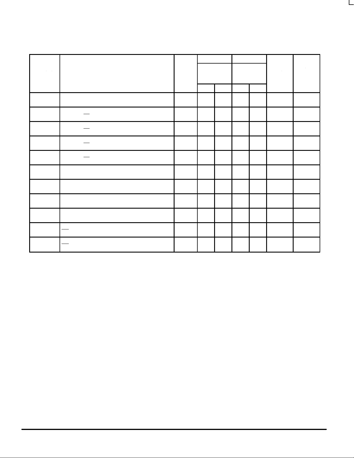
AC CHARACTERISTICS (For Figures and Waveforms — See Section 3)
74AC160 74AC160
Symbol
Parameter
VCC*
(V)
TA = +25°C
CL = 50 pF
TA = –40°C
to +85°C
CL = 50 pF
Unit
Fig.
No.
Min Max Min Max
Maximum Count
3.3 65 — 60 —
f
max
Frequency 5.0 110 — 95 —
MHz
3-3
Propagation Delay
3.3 2.0 12.0 1.5 14.0
t
PLH
CP to Qn (PE Input HIGH) 5.0 1.5 9.0 1.0 10.5
ns
3-6
Propagation Delay
3.3 2.0 12.0 1.5 14.0
t
PHL
CP to Qn (PE Input HIGH) 5.0 1.5 9.0 1.5 10.5
ns
3-6
Propagation Delay
3.3 2.0 12.0 1.5 14.0
t
PLH
CP to Qn (PE Input LOW) 5.0 1.5 9.0 1.0 10.5
ns
3-6
Propagation Delay
3.3 2.0 12.0 1.5 14.0
t
PHL
CP to Qn (PE Input LOW) 5.0 1.5 9.0 1.5 10.5
ns
3-6
Propagation Delay
3.3 3.0 15.0 2.5 17.5
t
PLH
CP to TC 5.0 2.0 11.0 1.5 12.5
ns
3-6
Propagation Delay
3.3 3.5 14.5 2.5 16.5
t
PHL
CP to TC 5.0 2.0 11.0 2.0 12.5
ns
3-6
Propagation Delay
3.3 2.0 10.5 1.5 12.5
t
PLH
CET to TC 5.0 1.5 7.5 1.0 9.0
ns
3-6
Propagation Delay
3.3 2.5 11.5 2.0 13.5
t
PHL
CET to TC 5.0 2.0 9.0 1.5 10.5
ns
3-6
Propagation Delay
3.3 2.0 12.0 1.5 13.5
t
PHL
MR to Qn (′AC160) 5.0 1.5 9.5 1.0 10.0
ns
3-6
Propagation Delay
3.3 3.5 15.0 3.0 17.0
t
PHL
MR to TC 5.0 2.5 12.0 2.0 13.5
ns
3-6
* Voltage Range 3.3 V is 3.3 V ±0.3 V.
Voltage Range 5.0 V is 5.0 V ±0.5 V.

MC74AC160 MC74ACT160 MC74AC162 MC74ACT162
5-6
FACT DATA
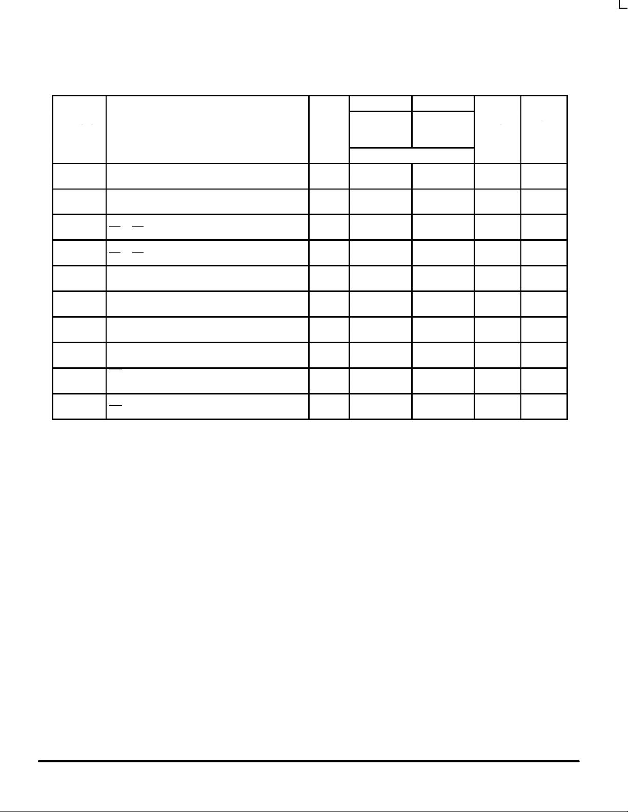
MC74AC162
AC CHARACTERISTICS (For Figures and Waveforms — See Section 3)
74AC162 74AC162
Symbol
Parameter
VCC*
(V)
TA = +25°C
CL = 50 pF
TA = –40°C
to +85°C
CL = 50 pF
Unit
Fig.
No.
Min Typ Max Min Max
Maximum Count
3.3 80 60
f
max
Frequency 5.0 125 100
MHz
3-3
Propagation Delay 3.3 2.0 12.0 1.5 13.5
t
PLH
CP to Qn (PE Input HIGH) 5.0 2.0 9.0 1.5 10.5
ns
3-6
Propagation Delay 3.3 2.0 12.0 1.5 13.5
t
PHL
CP to Qn (PE Input HIGH) 5.0 2.0 9.0 1.5 10.5
ns
3-6
Propagation Delay 3.3 2.0 12.0 1.5 13.5
t
PLH
CP to Qn (PE Input LOW) 5.0 2.0 9.0 1.5 10.5
ns
3-6
Propagation Delay 3.3 2.0 12.0 1.5 13.5
t
PHL
CP to Qn (PE Input LOW) 5.0 2.0 9.0 1.5 10.5
ns
3-6
Propagation Delay 3.3 2.0 15.0 1.5 17.0
t
PLH
CP to TC 5.0 2.0 11.0 1.5 13.0
ns
3-6
Propagation Delay 3.3 2.0 14.0 1.5 16.0
t
PHL
CP to TC 5.0 2.0 11.0 1.5 13.0
ns
3-6
Propagation Delay 3.3 2.0 10.0 1.5 11.5
t
PLH
CET to TC 5.0 2.0 7.0 1.5 8.5
ns
3-6
Propagation Delay 3.3 2.0 11.0 1.5 12.5
t
PHL
CET to TC 5.0 2.0 8.0 1.5 9.5
ns
3-6
*Voltage Range 3.3 V is 3.0 V ±0.3 V.
Voltage Range 5.0 V is 5.0 V ±0.5 V.
MC74AC160 MC74ACT160 MC74AC162 MC74ACT162
5-7
FACT DATA
MC74AC160
AC OPERATING REQUIREMENTS
74AC160 74AC160
Symbol
Parameter
VCC*
(V)
TA = +25°C
CL = 50 pF
TA = –40°C
to +85°C
CL = 50 pF
Unit
Fig.
No.
Guaranteed Maximum
Setup Time, HIGH or LOW
3.3 13.5 16.0
t
s
Pn to CP 5.0 8.5 10.5
ns
3-9
Hold Time, HIGH or LOW
3.3 –1.0 – 0.5
t
h
Pn to CP 5.0 0 0
ns
3-9
Setup Time, HIGH or LOW
3.3 11.5 14.0
t
s
PE or SR to CP 5.0 7.5 8.5
ns
3-9
Hold Time, HIGH or LOW
3.3 0 0
t
h
PE or SR to CP 5.0 0.5 1.0
ns
3-9
Setup Time, HIGH or LOW
3.3 6.0 7.0
t
s
CEP or CET to CP 5.0 4.5 5.0
ns
3-9
Hold Time, HIGH or LOW
3.3 0 0
t
h
CEP or CET to CP 5.0 0 0.5
ns
3-9
Clock Pulse Width (Load)
3.3 4.0 5.0
t
w
HIGH or LOW 5.0 3.0 3.5
ns
3-6
Clock Pulse Width (Count)
3.3 7.0 7.5
t
w
HIGH or LOW 5.0 4.5 5.5
ns
3-6
MR Pulse Width, LOW
3.3 5.5 7.5
t
w
(′AC160) 5.0 4.5 6.0
ns
3-6
Recovery Time
3.3 – 0.5 0
t
rec
MR to CP (′AC160) 5.0 0 0.5
ns
3-9
* Voltage Range 3.3 V is 3.3 V ±0.3 V.
Voltage Range 5.0 V is 5.0 V ±0.5 V.

MC74AC160 MC74ACT160 MC74AC162 MC74ACT162
5-8
FACT DATA
MC74AC162
AC OPERATING REQUIREMENTS
74AC162 74AC162
Symbol
Parameter
VCC*
(V)
TA = +25°C
CL = 50 pF
TA = –40°C
to +85°C
CL = 50 pF
Unit
Fig.
No.
Typ Guaranteed Minimum
Setup Time, HIGH or LOW 3.3 8.0 9.0
t
s
Pn to CP 5.0 5.0 6.0
ns
3-9
Hold Time, HIGH or LOW 3.3 0.5 1.0
t
h
Pn to CP 5.0 0.5 1.0
ns
3-9
Setup Time, HIGH or LOW 3.3 10.0 11.0
t
s
PE to CP 3.3 6.0 7.0
ns
3-9
Hold Time, HIGH or LOW 3.3 0.5 1.0
t
h
PE to CP 5.0 0.5 1.0
ns
3-9
Setup Time, HIGH or LOW 3.3 6.0 7.0
t
s
CEP or CET to CP 5.0 4.0 5.0
ns
3-9
Hold Time, HIGH or LOW 3.3 0.5 1.0
t
h
CEP or CET to CP 5.0 0.5 1.0
ns
3-9
Setup Time, HIGH or LOW 3.3 8.0 9.0
t
s
SR to CP 5.0 6.0 7.0
ns
3-9
Hold Time, HIGH or LOW 3.3 0.5 1.0
t
h
SR to CP 5.0 0.5 1.0
ns
3-9
Clock Pulse Width (Load) 3.3 5.5 6.0
t
w
HIGH or LOW 5.0 4.5 5.0
ns
3-6
Clock Pulse Width (Count) 3.3 5.0 5.5
t
w
HIGH or LOW 5.0 4.0 4.5
ns
3-6
*Voltage Range 3.3 V is 3.3 V ±0.3 V.
Voltage Range 5.0 V is 5.0 V ±0.5 V.

MC74AC160 MC74ACT160 MC74AC162 MC74ACT162
5-9
FACT DATA
DC CHARACTERISTICS
74ACT 74ACT
Symbol
Parameter
V
CC
(V)
TA = +25°C
TA =
–40°C to +85°C
Unit
Conditions
Typ Guaranteed Limits
V
IH
4.5 1.5 2.0 2.0
V
OUT
= 0.1 V
5.5 1.5 2.0 2.0
V
or VCC – 0.1 V
V
IL
4.5 1.5 0.8 0.8
V
OUT
= 0.1 V
5.5 1.5 0.8 0.8
V
or VCC – 0.1 V
V
OH
4.5 4.49 4.4 4.4
I
OUT
= –50 µA
5.5 5.49 5.4 5.4
V
*VIN = VIL or V
IH
4.5 3.86 3.76 V
–24 mA
5.5 4.86 4.76
I
OH
–24 mA
V
OL
4.5 0.001 0.1 0.1
I
OUT
= 50 µA
5.5 0.001 0.1 0.1
V
*VIN = VIL or V
IH
4.5 0.36 0.44 V
24 mA
5.5 0.36 0.44
I
OL
24 mA
I
IN
5.5
±0.1
±1.0
µA
VI = VCC, GND
∆I
CCT
Additional Max. ICC/Input 5.5 0.6 1.5 mA VI = VCC – 2.1 V
I
OLD
5.5 75 mA V
OLD
= 1.65 V Max
I
OHD
Output Current
5.5 –75 mA V
OHD
= 3.85 V Min
I
CC
5.5
8.080µA
VIN = VCC or GND
* All outputs loaded; thresholds on input associated with output under test.
†Maximum test duration 2.0 ms, one output loaded at a time.
Minimum High Level
Input Voltage
Maximum Low Level
Input Voltage
Minimum High Level
Output Voltage
Maximum Low Level
Output Voltage
Maximum Input
Leakage Current
†Minimum Dynamic
Maximum Quiescent
Supply Current
MC74AC160 MC74ACT160 MC74AC162 MC74ACT162
5-10
FACT DATA
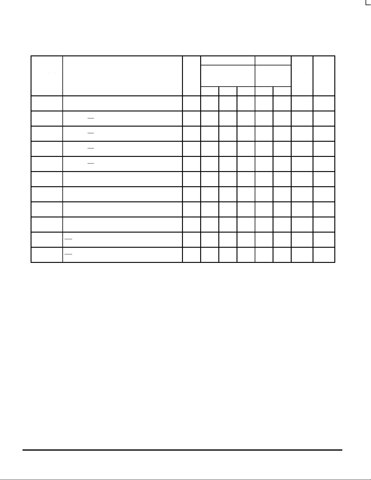
MC74ACT160
AC CHARACTERISTICS (For Figures and Waveforms — See Section 3)
74ACT160 74ACT160
Symbol
Parameter
VCC*
(V)
TA = +25°C
CL = 50 pF
TA = –40°C
to +85°C
CL = 50 pF
Unit
Fig.
No.
Min Typ Max Min Max
Maximum Count
f
max
Frequency
5.0
120
100
MHz
3-3
Propagation Delay
t
PLH
CP to Qn (PE Input HIGH)
5.0
2.0
6.0
10.0
2.0
11.0ns3-6
Propagation Delay
t
PHL
CP to Qn (PE Input HIGH)
5.0
2.0
6.0
10.0
2.0
11.0ns3-6
Propagation Delay
t
PLH
CP to Qn (PE Input LOW)
5.0
2.0
6.0
10.0
2.0
11.0ns3-6
Propagation Delay
t
PHL
CP to Qn (PE Input LOW)
5.0
2.0
6.0
10.0
2.0
11.0ns3-6
Propagation Delay
t
PLH
CP to TC
5.0
2.0
8.0
12.0
2.0
14.0ns3-6
Propagation Delay
t
PHL
CP to TC
5.0
2.0
8.0
12.0
2.0
14.0ns3-6
Propagation Delay
t
PLH
CET to TC
5.0
2.0
6.0
8.5
2.0
9.5ns3-6
Propagation Delay
t
PHL
CET to TC
5.0
2.0
7.0
9.5
2.0
11.0ns3-6
Propagation Delay
t
PHL
MR to Qn (′AC160)
5.0
1.5
6.0
9.5
1.5
11.0ns3-6
Propagation Delay
t
PHL
MR to TC
5.0
2.5—13.0
2.5
14.0ns3-6
* Voltage Range 5.0 V is 5.0 V ±0.5 V.

MC74AC160 MC74ACT160 MC74AC162 MC74ACT162
5-11
FACT DATA
MC74ACT162
AC CHARACTERISTICS (For Figures and Waveforms — See Section 3)
74ACT162 74ACT162
Symbol
Parameter
VCC*
(V)
TA = +25°C
CL = 50 pF
TA = –40°C
to +85°C
CL = 50 pF
Unit
Fig.
No.
Min Typ Max Min Max
Maximum Count
f
max
Frequency
5.0
120
100
MHz
3-3
Propagation Delay
t
PLH
CP to Qn (PE Input HIGH)
5.0
2.0
6.0
10.0
2.0
11.5ns3-6
Propagation Delay
t
PHL
CP to Qn (PE Input HIGH)
5.0
2.0
6.0
10.0
2.0
11.0ns3-6
Propagation Delay
t
PLH
CP to Qn (PE Input LOW)
5.0
2.0
6.0
10.0
2.0
11.5ns3-6
Propagation Delay
t
PHL
CP to Qn (PE Input LOW)
5.0
2.0
6.0
10.0
2.0
11.0ns3-6
Propagation Delay
t
PLH
CP to TC
5.0
2.0
8.0
13.0
2.0
14.5ns3-6
Propagation Delay
t
PHL
CP to TC
5.0
2.0
8.0
13.0
2.0
14.5ns3-6
Propagation Delay
t
PLH
CET to TC
5.0
2.0
6.0
9.0
2.0
10.5ns3-6
Propagation Delay
t
PHL
CET to TC
5.0
2.0
6.0
9.0
2.0
10.5ns3-6
* Voltage Range 5.0 V is 5.0 V ±0.5 V. 3

MC74AC160 MC74ACT160 MC74AC162 MC74ACT162
5-12
FACT DATA
MC74ACT160
AC OPERATING REQUIREMENTS
74ACT160 74ACT160
Symbol
Parameter
VCC*
(V)
TA = +25°C
CL = 50 pF
TA = –40°C
to +85°C
CL = 50 pF
Unit
Fig.
No.
Typ Guaranteed Maximum
Setup Time, HIGH or LOW
t
s
Pn to CP
5.0
4.0
6.5
8.0
ns
3-9
Hold Time, HIGH or LOW
t
h
Pn to CP
5.0
–4.0
–0.50ns
3-9
Setup Time, HIGH or LOW
t
s
PE or MR to CP
5.0
4.0
8.5
10.5
ns
3-9
Hold Time, HIGH or LOW
t
h
PE or MR to CP
5.0
–4.000
ns
3-9
Setup Time, HIGH or LOW
t
s
CEP or CET to CP
5.0
3.0
6.0
7.0
ns
3-9
Hold Time, HIGH or LOW
t
h
CEP or CET to CP
5.0
–3.000
ns
3-9
Clock Pulse Width (Load)
t
w
HIGH or LOW
5.0
3.0
4.0
4.0
ns
3-6
Clock Pulse Width (Count)
t
w
HIGH or LOW
5.0
3.0
4.0
4.0
ns
3-6
MR Pulse Width, LOW
t
w
(′ACT160)
5.0
2.0
4.0
6.0
ns
3-6
Recovery Time
t
rec
MR to CP (′ACT160)
5.0
–1.000
ns
3-9
* Voltage Range 5.0 V is 5.0 V ±0.5 V.

MC74AC160 MC74ACT160 MC74AC162 MC74ACT162
5-13
FACT DATA
MC74ACT162
AC OPERATING REQUIREMENTS
74ACT162 74ACT162
Symbol
Parameter
VCC*
(V)
TA = +25°C
CL = 50 pF
TA = –40°C
to +85°C
CL = 50 pF
Unit
Fig.
No.
Typ Guaranteed Maximum
Setup Time, HIGH or LOW
t
s
Pn to CP
5.0
4.0
7.0
10.0
ns
3-9
Hold Time, HIGH or LOW
t
h
Pn to CP
5.0
–3.0
–1.00ns
3-9
Setup Time, HIGH or LOW
t
s
PE to CP
5.0
4.0
7.0
10.0
ns
3-9
Hold Time, HIGH or LOW
t
h
PE to CP
5.0
–3.0
–1.00ns
3-9
Setup Time, HIGH or LOW
t
s
SR to CP
5.0
5.01011.5
ns
3-9
Hold Time, HIGH or LOW
t
h
SR to CP
5.0
–5.000
ns
3-9
Setup Time, HIGH or LOW
t
s
CET to CP
5.0
3.0
6.0
7.0
ns
3-9
Hold Time, HIGH or LOW
t
h
CET to CP
5.0
–3.000
ns
3-9
Clock Pulse Width (Load)
t
w
HIGH or LOW
5.0
2.0
4.5
5.0
ns
3-6
Clock Pulse Width (Count)
t
w
HIGH or LOW
5.0
2.0
4.0
4.5
ns
3-6
* Voltage Range 5.0 V is 5.0 V ±0.5 V.
CAPACITANCE
Symbol Parameter
Value
Typ
Unit Test Conditions
C
IN
Input Capacitance 4.5 pF VCC = 5.0 V
C
PD
Power Dissipation Capacitance 45 pF VCC = 5.0 V
MC74AC160 MC74ACT160 MC74AC162 MC74ACT162
5-14
FACT DATA
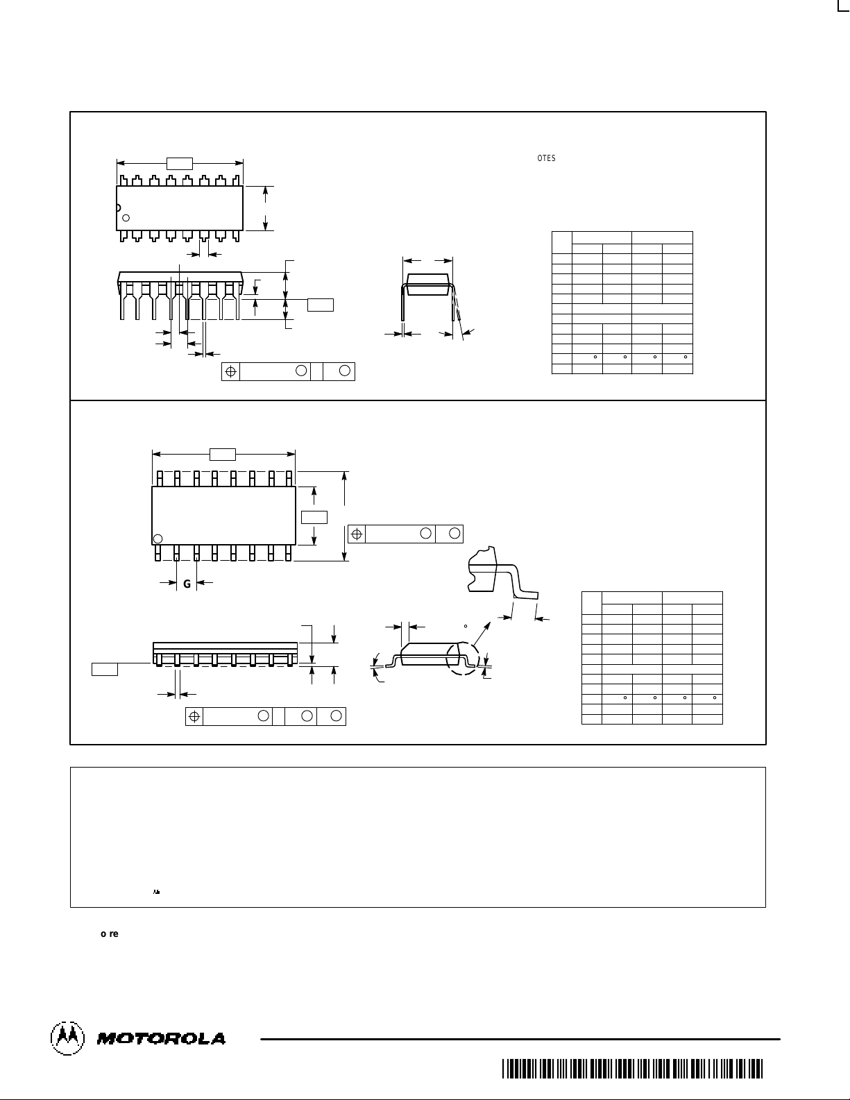
OUTLINE DIMENSIONS
N SUFFIX
PLASTIC DIP PACKAGE
CASE 648–08
ISSUE R
D SUFFIX
PLASTIC SOIC PACKAGE
CASE 751B–05
ISSUE J
NOTES:
1. DIMENSIONING AND TOLERANCING PER
ANSI Y14.5M, 1982.
2. CONTROLLING DIMENSION: MILLIMETER.
3. DIMENSIONS A AND B DO NOT INCLUDE
MOLD PROTRUSION.
4. MAXIMUM MOLD PROTRUSION 0.15 (0.006)
PER SIDE.
5. DIMENSION D DOES NOT INCLUDE DAMBAR
PROTRUSION. ALLOWABLE DAMBAR
PROTRUSION SHALL BE 0.127 (0.005) TOTAL
IN EXCESS OF THE D DIMENSION AT
MAXIMUM MATERIAL CONDITION.
1 8
16 9
SEATING
PLANE
F
J
M
R
X 45
_
G
8 PLP
–B–
–A–
M
0.25 (0.010) B
S
–T–
D
K
C
16 PL
S
B
M
0.25 (0.010) A
S
T
DIM MIN MAX MIN MAX
INCHESMILLIMETERS
A 9.80 10.00 0.386 0.393
B 3.80 4.00 0.150 0.157
C 1.35 1.75 0.054 0.068
D 0.35 0.49 0.014 0.019
F 0.40 1.25 0.016 0.049
G 1.27 BSC 0.050 BSC
J 0.19 0.25 0.008 0.009
K 0.10 0.25 0.004 0.009
M 0 7 0 7
P 5.80 6.20 0.229 0.244
R 0.25 0.50 0.010 0.019
_ _ _ _
NOTES:
1. DIMENSIONING AND TOLERANCING PER ANSI
Y14.5M, 1982.
2. CONTROLLING DIMENSION: INCH.
3. DIMENSION L TO CENTER OF LEADS WHEN
FORMED PARALLEL.
4. DIMENSION B DOES NOT INCLUDE MOLD FLASH.
5. ROUNDED CORNERS OPTIONAL.
–A–
B
F
C
S
H
G
D
J
L
M
16 PL
SEATING
1 8
916
K
PLANE
–T–
M
A
M
0.25 (0.010) T
DIM MIN MAX MIN MAX
MILLIMETERSINCHES
A 0.740 0.770 18.80 19.55
B 0.250 0.270 6.35 6.85
C 0.145 0.175 3.69 4.44
D 0.015 0.021 0.39 0.53
F 0.040 0.70 1.02 1.77
G 0.100 BSC 2.54 BSC
H 0.050 BSC 1.27 BSC
J 0.008 0.015 0.21 0.38
K 0.110 0.130 2.80 3.30
L 0.295 0.305 7.50 7.74
M 0 10 0 10
S 0.020 0.040 0.51 1.01
____
How to reach us:
USA/EUROPE: Motorola Literature Distribution; JAPAN: Nippon Motorola Ltd.; Tatsumi–SPD–JLDC, Toshikatsu Otsuki,
P.O. Box 20912; Phoenix, Arizona 85036. 1–800–441–2447 6F Seibu–Butsuryu–Center, 3–14–2 Tatsumi Koto–Ku, Tokyo 135, Japan. 03–3521–8315
MFAX: RMFAX0@email.sps.mot.com –TOUCHTONE (602) 244–6609 HONG KONG: Motorola Semiconductors H.K. Ltd.; 8B Tai Ping Industrial Park,
INTERNET: http://Design–NET.com 51 Ting Kok Road, Tai Po, N.T., Hong Kong. 852–26629298
Motorola reserves the right to make changes without further notice to any products herein. Motorola makes no warranty , representation or guarantee regarding
the suitability of its products for any particular purpose, nor does Motorola assume any liability arising out of the application or use of any product or circuit, and
specifically disclaims any and all liability , including without limitation consequential or incidental damages. “Typical” parameters can and do vary in different
applications. All operating parameters, including “T ypicals” must be validated for each customer application by customer’s technical experts. Motorola does
not convey any license under its patent rights nor the rights of others. Motorola products are not designed, intended, or authorized for use as components in
systems intended for surgical implant into the body, or other applications intended to support or sustain life, or for any other application in which the failure of
the Motorola product could create a situation where personal injury or death may occur. Should Buyer purchase or use Motorola products for any such
unintended or unauthorized application, Buyer shall indemnify and hold Motorola and its officers, employees, subsidiaries, affiliates, and distributors harmless
against all claims, costs, damages, and expenses, and reasonable attorney fees arising out of, directly or indirectly, any claim of personal injury or death
associated with such unintended or unauthorized use, even if such claim alleges that Motorola was negligent regarding the design or manufacture of the part.
Motorola and are registered trademarks of Motorola, Inc. Motorola, Inc. is an Equal Opportunity/Affirmative Action Employer.
MC74AC160/D
*MC74AC160/D*
◊
 Loading...