

Motorola MC74ACT162N, MC74ACT160N, MC74ACT160D, MC74AC162D, MC74AC162N Datasheet
...
5-1
FACT DATA
The MC74AC160/74ACT160 and MC74AC162/74ACT162 are high-speed
synchronous decade counters operating in the BCD (8421) sequence. They
are synchronously presettable for application in programmable dividers and have
two types of Count Enable inputs plus a Terminal Count output for versatility in
forming synchronous multistage counters. The MC74AC160/74ACT160 has an
asynchronous Master Reset input that overrides all other inputs and forces the
outputs LOW. The MC74AC162/74ACT162 has a Synchronous Reset input that
overrides counting and parallel loading and allows all outputs to be simultaneously
reset on the rising edge of the clock.
• Synchronous Counting and Loading
• High-Speed Synchronous Expansion
• Typical Count Rate of 120 MHz
• Outputs Source/Sink 24 mA
• ′ACT160 and ′ACT162 Have TTL Compatible Inputs
1516 14 13 12 11 10
21 3 4 5 6 7
V
CC
9
8
*R
P
0
CP P1P2P3CEP GND
TC Q0Q1Q2Q3CET PE
PIN NAMES
CEP Count Enable Parallel Input
CET Count Enable Trickle Input
CP Clock Pulse Input
MR
(′160) Asynchronous Master Reset Input
SR
(′162) Synchronous Reset Input
P0–P3Parallel Data Inputs
PE
Parallel Enable Input
Q0–Q3Flip-Flop Outputs
TC Terminal Count Output
SYNCHRONOUS
PRESETTABLE
BCD DECADE COUNTER
N SUFFIX
CASE 648-08
PLASTIC
D SUFFIX
CASE 751B-05
PLASTIC
LOGIC SYMBOL
PE P0P1P
2
CEP
P
3
CET
CP
*R Q0Q1Q2Q
3
TC
*MR for ′160
*SR
for ′162
MC74AC160 MC74ACT160 MC74AC162 MC74ACT162
5-2
FACT DATA
FUNCTIONAL DESCRIPTION
The MC74AC160/74ACT160 and MC74AC162/74ACT162
count modulo-10 in the BCD (8421) sequence. From state 9
(HLLH) they increment to state 0 (LLLL). The clock inputs of
all flip-flops are driven in parallel through a clock buffer. Thus
all changes of the Q outputs (except due to Master Reset of the
′160) occur as a result of, and synchronous with, the
LOW-to-HIGH transition of the CP input signal. The circuits
have four fundamental modes of operation, in order of
precedence: asynchronous reset (′160), synchronous reset
(′162), parallel load, count-up and hold. Five control inputs —
Master Reset (MR
, ′160), Synchronous Reset (SR,′162),
Parallel Enable (PE
), Count Enable Parallel (CEP) and Count
Enable Trickle (CET) — determine the mode of operation, as
shown in the Mode Select Table. A LOW signal on MR
overrides all other inputs and asynchronously forces all
outputs LOW. A LOW signal on SR
overrides counting and
parallel loading and allows all outputs to go LOW on the next
rising edge of CP . A LOW signal on PE
overrides counting and
allows information on the Parallel Data (Pn) inputs to be loaded
into the flip-flops on the next rising edge of CP . With PE
and MR
(′160) or SR (′162) HIGH, CEP and CET permit counting when
both are HIGH. Conversely, a LOW signal on either CEP or
CET inhibits counting.
The MC74AC160/74ACT160 and MC74AC162/74ACT162
use D-type edge-triggered flip-flops and changing the SR
, PE,
CEP and CET inputs when the CP is in either state does not
cause errors, provided that the recommended setup and hold
times, with respect to the rising edge of CP, are observed.
The T erminal Count (TC) output is HIGH when CET is HIGH
and counter is in state 9. To implement synchronous
multistage counters, the TC outputs can be used with the CEP
and CET inputs in two different ways. Please refer to the
MC74AC568 data sheet. The TC output is subject to decoding
spikes due to internal race conditions and is therefore not
recommended for use as a clock or asynchronous reset for
flip-flops, counters or registers. In the MC74AC160/74ACT160
and MC74AC162/74ACT162 decade counters, the TC output i s
fully decoded and can only be HIGH in state 9. If a decade
counter is preset to an illegal state, or assumes an illegal state
when power is applied, it will return to the normal sequence
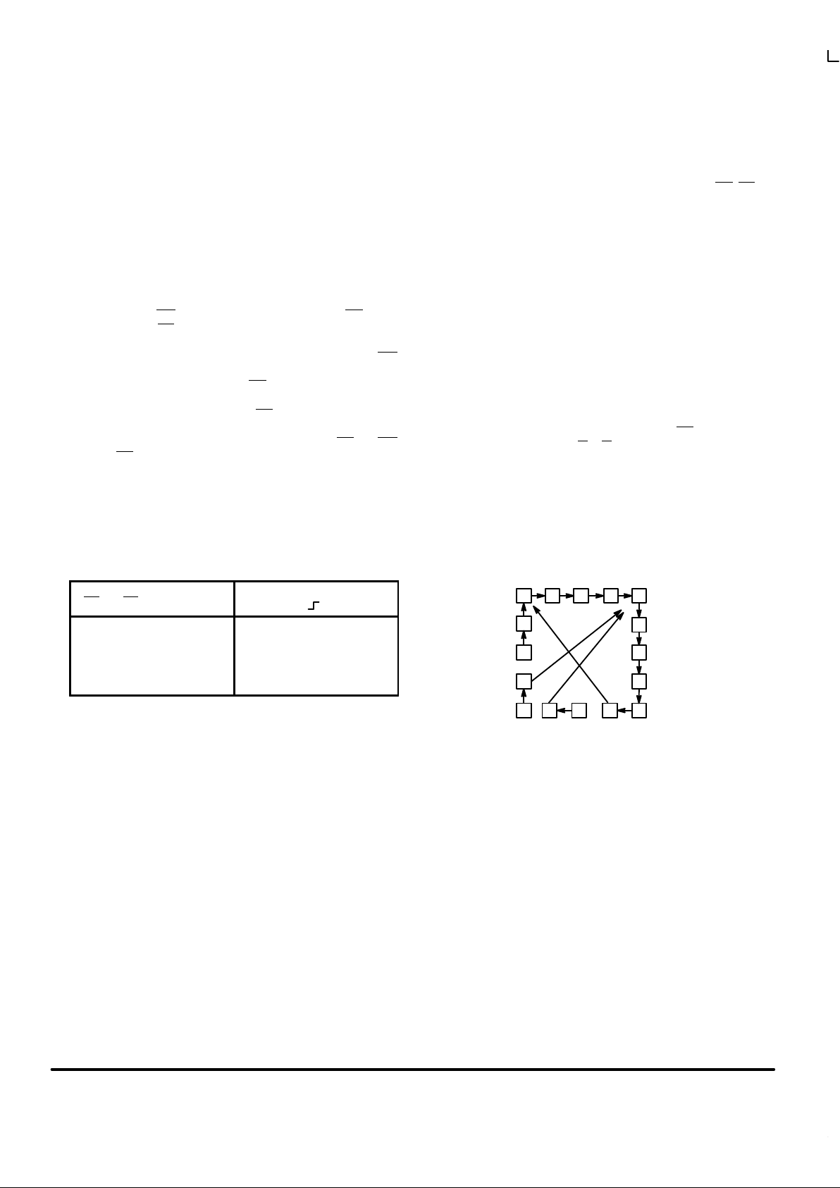
within two counts, as shown in the State Diagram.
Logic Equations:Count Enable = CEP
• CET• PE
TC = Q
0
• Q1• Q2• Q3• CET
MODE SELECT TABLE
*SR PE CET CEP
Action on the Rising
Clock Edge ( )
L X X X Reset (Clear)
H L X X Load (Pn → Qn)
H H H H Count (Increment)
H H L X No Change (Hold)
H H X L No Change (Hold)
*For ′162 only
H = HIGH Voltage Level
L = LOW Voltage Level
X = Immaterial
STATE DIAGRAM
0 1 2 4
5
6
7
89101112
13
14
15
3
MC74AC160 MC74ACT160 MC74AC162 MC74ACT162
5-3
FACT DATA
C
D
PE
P
0
P
1
P
2
CEP
P
3
CET
CP
Q
0
Q
1
Q
2
Q
3
TC
MR ′160
SR
′162
′
162
ONLY
′162
CP
Q
0
Q
0
CP
DETAIL A
DETAIL A DETAIL A DETAIL A
D CP D
Q Q
LOGIC DIAGRAM
Please note that this diagram is provided only for the understanding of logic
operations and should not be used to estimate propagation delays.
′
160
ONLY
′160
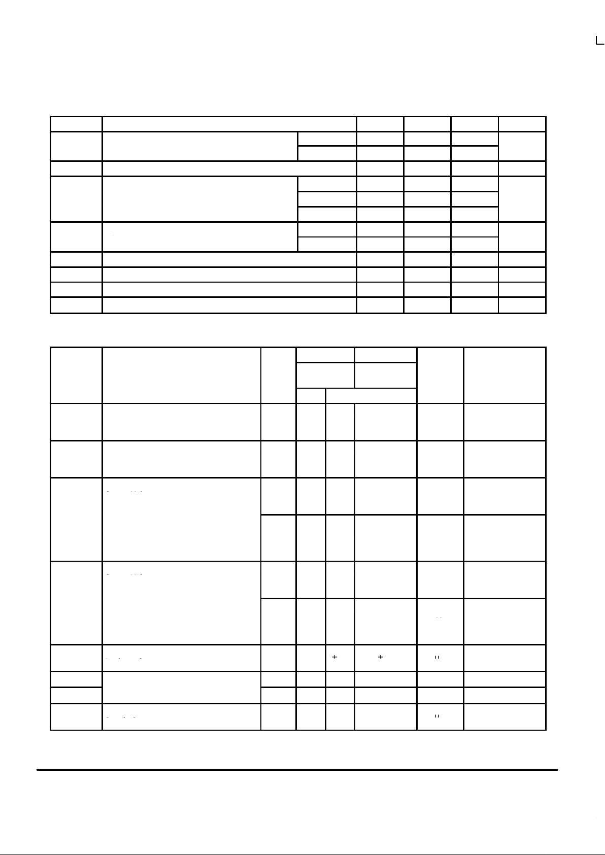
MAXIMUM RATINGS*
Symbol Parameter Value Unit
V
CC
DC Supply Voltage (Referenced to GND) –0.5 to +7.0 V
V
in
DC Input Voltage (Referenced to GND) –0.5 to VCC +0.5 V
V
out
DC Output Voltage (Referenced to GND) –0.5 to VCC +0.5 V
I
in
DC Input Current, per Pin ±20 mA
I
out
DC Output Sink/Source Current, per Pin ±50 mA
I
CC
DC VCC or GND Current per Output Pin ±50 mA
T
stg
Storage Temperature –65 to +150 °C
* Maximum Ratings are those values beyond which damage to the device may occur. Functional operation should be restricted to the Recommended
Operating Conditions.
MC74AC160 MC74ACT160 MC74AC162 MC74ACT162
5-4
FACT DATA
RECOMMENDED OPERATING CONDITIONS
Symbol Parameter Min Typ Max Unit
′AC 2.0 5.0 6.0
VCCSupply Voltage
′ACT 4.5 5.0 5.5
V
Vin, V
out
DC Input Voltage, Output Voltage (Ref. to GND) 0 V
CC
V
VCC @ 3.0 V 150
tr, t
f
Input Rise and Fall Time (Note 1)
′AC Devices except Schmitt Inputs
VCC @ 4.5 V 40 ns/V
r
, t
f
′AC Devices except Schmitt Inputs
VCC @ 5.5 V 25
Input Rise and Fall Time (Note 2)
VCC @ 4.5 V 10
tr, t
f
Input Rise and Fall Time (Note 2)
′ACT Devices except Schmitt Inputs
VCC @ 5.5 V 8.0
ns/V
T
J
Junction Temperature (PDIP) 140 °C
T
A
Operating Ambient Temperature Range –40 25 85 °C
I
OH
Output Current — High –24 mA
I
OL
Output Current — Low 24 mA
1. Vin from 30% to 70% VCC; see individual Data Sheets for devices that differ from the typical input rise and fall times.
2. Vin from 0.8 V to 2.0 V; see individual Data Sheets for devices that differ from the typical input rise and fall times.
DC CHARACTERISTICS
74AC 74AC
Symbol
Parameter
V
CC
(V)
TA = +25°C
TA =
–40°C to +85°C
Unit
Conditions
Typ Guaranteed Limits
V
IH
Minimum High Level
3.0 1.5 2.1 2.1 V
OUT
= 0.1 V
Input Voltage
4.5 2.25 3.15 3.15 V or VCC – 0.1 V
5.5 2.75 3.85 3.85
V
IL
Maximum Low Level
3.0 1.5 0.9 0.9 V
OUT
= 0.1 V
Input Voltage
4.5 2.25 1.35 1.35 V or VCC – 0.1 V
5.5 2.75 1.65 1.65
V
OH
Minimum High Level
3.0 2.99 2.9 2.9 I
OUT
= –50 µA
Output Voltage
4.5 4.49 4.4 4.4 V
5.5 5.49 5.4 5.4
*VIN = VIL or V
IH
3.0 2.56 2.46
–12 mA
4.5 3.86 3.76
V
I
OH
–24 mA
5.5 4.86 4.76 –24 mA
V
OL
Maximum Low Level
3.0 0.002 0.1 0.1 I
OUT
= 50 µA
Output Voltage
4.5 0.001 0.1 0.1 V
5.5 0.001 0.1 0.1
*VIN = VIL or V
IH
3.0 0.36 0.44
12 mA
4.5 0.36 0.44
V
I
OL
24 mA
5.5 0.36 0.44 24 mA
I
IN
Maximum Input
Leakage Current
5.5
±0.1
±1.0
µA
VI = VCC, GND
I
OLD
†Minimum Dynamic
5.5 75 mA V
OLD
= 1.65 V Max
I
OHD
Output Current
5.5 –75 mA V
OHD
= 3.85 V Min
I
CC
Maximum Quiescent
Supply Current
5.5
8.080µA
VIN = VCC or GND
* All outputs loaded; thresholds on input associated with output under test.
†Maximum test duration 2.0 ms, one output loaded at a time.
Note: IIN and ICC @ 3.0 V are guaranteed to be less than or equal to the respective limit @ 5.5 V VCC.
MC74AC160 MC74ACT160 MC74AC162 MC74ACT162
5-5
FACT DATA
MC74AC160
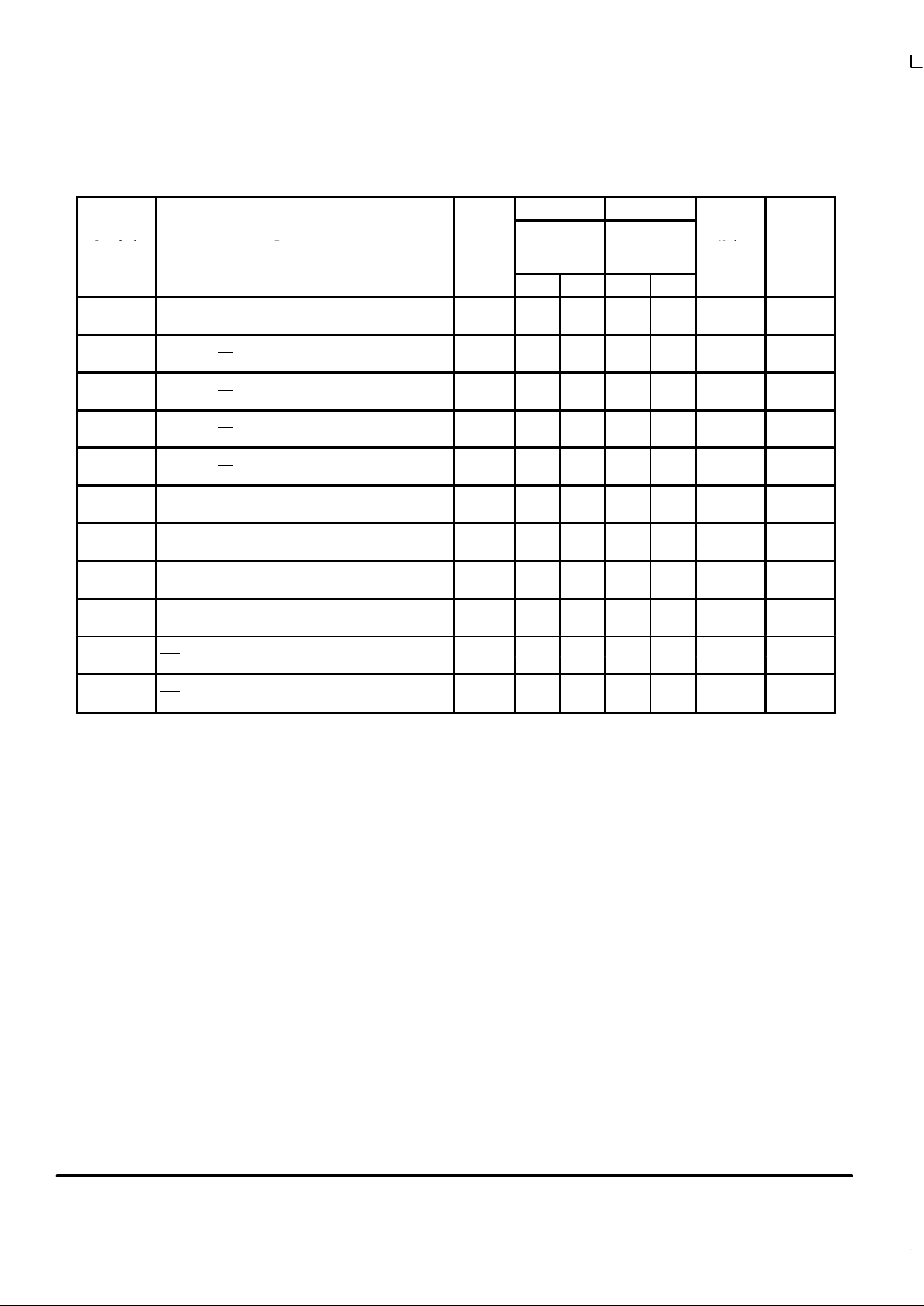
AC CHARACTERISTICS (For Figures and Waveforms — See Section 3)
74AC160 74AC160
Symbol
Parameter
VCC*
(V)
TA = +25°C
CL = 50 pF
TA = –40°C
to +85°C
CL = 50 pF
Unit
Fig.
No.
Min Max Min Max
Maximum Count
3.3 65 — 60 —
f
max
Frequency 5.0 110 — 95 —
MHz
3-3
Propagation Delay
3.3 2.0 12.0 1.5 14.0
t
PLH
CP to Qn (PE Input HIGH) 5.0 1.5 9.0 1.0 10.5
ns
3-6
Propagation Delay
3.3 2.0 12.0 1.5 14.0
t
PHL
CP to Qn (PE Input HIGH) 5.0 1.5 9.0 1.5 10.5
ns
3-6
Propagation Delay
3.3 2.0 12.0 1.5 14.0
t
PLH
CP to Qn (PE Input LOW) 5.0 1.5 9.0 1.0 10.5
ns
3-6
Propagation Delay
3.3 2.0 12.0 1.5 14.0
t
PHL
CP to Qn (PE Input LOW) 5.0 1.5 9.0 1.5 10.5
ns
3-6
Propagation Delay
3.3 3.0 15.0 2.5 17.5
t
PLH
CP to TC 5.0 2.0 11.0 1.5 12.5
ns
3-6
Propagation Delay
3.3 3.5 14.5 2.5 16.5
t
PHL
CP to TC 5.0 2.0 11.0 2.0 12.5
ns
3-6
Propagation Delay
3.3 2.0 10.5 1.5 12.5
t
PLH
CET to TC 5.0 1.5 7.5 1.0 9.0
ns
3-6
Propagation Delay
3.3 2.5 11.5 2.0 13.5
t
PHL
CET to TC 5.0 2.0 9.0 1.5 10.5
ns
3-6
Propagation Delay
3.3 2.0 12.0 1.5 13.5
t
PHL
MR to Qn (′AC160) 5.0 1.5 9.5 1.0 10.0
ns
3-6
Propagation Delay
3.3 3.5 15.0 3.0 17.0
t
PHL
MR to TC 5.0 2.5 12.0 2.0 13.5
ns
3-6
* Voltage Range 3.3 V is 3.3 V ±0.3 V.
Voltage Range 5.0 V is 5.0 V ±0.5 V.
 Loading...