

Motorola MC68HC705P9S, MC68HC705P9VDW, MC68HC705P9VP, MC68HC705P9MS, MC68HC705P9CS Datasheet
...
MC68HC705P9/D
REV. 3
MC68HC705P9
HCMOS Microcontroller Unit
TECHNICAL DATA

M O T O R O L A
CSIC
MICROCONTROLLERS

List of Sections
Table of Contents . . . . . . . . . . . . . . . . . . . . . . . . . 5
Introduction . . . . . . . . . . . . . . . . . . . . . . . . . . . . . . 9
Pin Descriptions . . . . . . . . . . . . . . . . . . . . . . . . . . 13
Memory . . . . . . . . . . . . . . . . . . . . . . . . . . . . . . . . 19
Central Processor Unit (CPU) . . . . . . . . . . . . . . . 33
Resets and Interrupts. . . . . . . . . . . . . . . . . . . . . . 55
Low-Power Modes. . . . . . . . . . . . . . . . . . . . . . . . 65
Parallel I/O Ports . . . . . . . . . . . . . . . . . . . . . . . . . 71
Computer Operating Properly
Watchdog (COP) . . . . . . . . . . . . . . . . . . . . . . 85
Timer. . . . . . . . . . . . . . . . . . . . . . . . . . . . . . . . . . . 89
Serial Input/Output Port (SIOP). . . . . . . . . . . . . 107
Analog-to-Digital Converter (ADC). . . . . . . . . 121
Specifications . . . . . . . . . . . . . . . . . . . . . . . . . . 131
Index . . . . . . . . . . . . . . . . . . . . . . . . . . . . . . . . . 145
Literature Updates. . . . . . . . . . . . . . . . . . . . . . . 151
Motorola, Inc., 1996
MOTOROLA 3
List of Sections
List of Modules
List of Modules
All M68HC05 microcontroller units (MCUs) are customer-specified
modular designs. To meet customer requirements, Motorola is
constantly designing new modules and new versions of existing
modules. The following table shows the version levels of the modules in
the MC68HC705P9 MCU.
Module Version
Central Processor Unit (CPU) HC05CPU
Timer TIM1IC1OC_A
Serial Input/Output Port (SIOP) SIOP_A
Computer Operating Properly Watchdog (COP) COP0COP
Analog-to-Digital Converter (ADC) ATD4X8NVRL
Revision History
The following table summarizes differences between this revision and
the previous revision of this Technical Data manual.
Previous
Revision
Current
Revision
Date 11/95
Changes Format and organizational changes
Location Throughout
2.0
3.0
4 MOTOROLA

Table of Contents
List of Sections List of Modules . . . . . . . . . . . . . . . . . . . . . . . . . . . . . . . . . . . . . . . . . . .4
Revision History. . . . . . . . . . . . . . . . . . . . . . . . . . . . . . . . . . . . . . . . . . .4
Introduction Contents . . . . . . . . . . . . . . . . . . . . . . . . . . . . . . . . . . . . . . . . . . . . . . . .9
Features . . . . . . . . . . . . . . . . . . . . . . . . . . . . . . . . . . . . . . . . . . . . . . .10
Structure . . . . . . . . . . . . . . . . . . . . . . . . . . . . . . . . . . . . . . . . . . . . . . .11
Package Types and Order Numbers. . . . . . . . . . . . . . . . . . . . . . . . . .12
Programmable Options . . . . . . . . . . . . . . . . . . . . . . . . . . . . . . . . . . . .12
Pin Descriptions Contents . . . . . . . . . . . . . . . . . . . . . . . . . . . . . . . . . . . . . . . . . . . . . . .13
Pin Assignments . . . . . . . . . . . . . . . . . . . . . . . . . . . . . . . . . . . . . . . . .14
Pin Functions. . . . . . . . . . . . . . . . . . . . . . . . . . . . . . . . . . . . . . . . . . . .15
Memory Contents . . . . . . . . . . . . . . . . . . . . . . . . . . . . . . . . . . . . . . . . . . . . . . .19
Features . . . . . . . . . . . . . . . . . . . . . . . . . . . . . . . . . . . . . . . . . . . . . . .19
Memory Map . . . . . . . . . . . . . . . . . . . . . . . . . . . . . . . . . . . . . . . . . . . .20
Input/Output Register Summary . . . . . . . . . . . . . . . . . . . . . . . . . . . . .21
RAM. . . . . . . . . . . . . . . . . . . . . . . . . . . . . . . . . . . . . . . . . . . . . . . . . . .24
EPROM/OTPROM. . . . . . . . . . . . . . . . . . . . . . . . . . . . . . . . . . . . . . . . . . . . . . . . . .25
Mask Option Register . . . . . . . . . . . . . . . . . . . . . . . . . . . . . . . . . . . . .31
CPU Contents . . . . . . . . . . . . . . . . . . . . . . . . . . . . . . . . . . . . . . . . . . . . . . .33
Features . . . . . . . . . . . . . . . . . . . . . . . . . . . . . . . . . . . . . . . . . . . . . . .34
Introduction . . . . . . . . . . . . . . . . . . . . . . . . . . . . . . . . . . . . . . . . . . . . .34
MOTOROLA Table of Contents 5

Table of Contents
CPU Control Unit. . . . . . . . . . . . . . . . . . . . . . . . . . . . . . . . . . . . . . . . .36
Arithmetic/Logic Unit . . . . . . . . . . . . . . . . . . . . . . . . . . . . . . . . . . . . . .36
CPU Registers. . . . . . . . . . . . . . . . . . . . . . . . . . . . . . . . . . . . . . . . . . .36
Instruction Set . . . . . . . . . . . . . . . . . . . . . . . . . . . . . . . . . . . . . . . . . . .40
Resets and
Interrupts
Low-Power Modes Contents . . . . . . . . . . . . . . . . . . . . . . . . . . . . . . . . . . . . . . . . . . . . . . .65
Parallel I/O Ports Contents . . . . . . . . . . . . . . . . . . . . . . . . . . . . . . . . . . . . . . . . . . . . . . .71
Contents . . . . . . . . . . . . . . . . . . . . . . . . . . . . . . . . . . . . . . . . . . . . . . .55
Resets . . . . . . . . . . . . . . . . . . . . . . . . . . . . . . . . . . . . . . . . . . . . . . . . .56
Low-Voltage Protection . . . . . . . . . . . . . . . . . . . . . . . . . . . . . . . . . . . .58
Interrupts . . . . . . . . . . . . . . . . . . . . . . . . . . . . . . . . . . . . . . . . . . . . . . .59
Stop Mode. . . . . . . . . . . . . . . . . . . . . . . . . . . . . . . . . . . . . . . . . . . . . .65
Wait Mode . . . . . . . . . . . . . . . . . . . . . . . . . . . . . . . . . . . . . . . . . . . . . .68
Data-Retention Mode . . . . . . . . . . . . . . . . . . . . . . . . . . . . . . . . . . . . .70
Introduction . . . . . . . . . . . . . . . . . . . . . . . . . . . . . . . . . . . . . . . . . . . . .72
Port A. . . . . . . . . . . . . . . . . . . . . . . . . . . . . . . . . . . . . . . . . . . . . . . . . .73
Port B. . . . . . . . . . . . . . . . . . . . . . . . . . . . . . . . . . . . . . . . . . . . . . . . . .76
Port C . . . . . . . . . . . . . . . . . . . . . . . . . . . . . . . . . . . . . . . . . . . . . . . . .79
Port D . . . . . . . . . . . . . . . . . . . . . . . . . . . . . . . . . . . . . . . . . . . . . . . . .82
COP Contents . . . . . . . . . . . . . . . . . . . . . . . . . . . . . . . . . . . . . . . . . . . . . . .85
Features . . . . . . . . . . . . . . . . . . . . . . . . . . . . . . . . . . . . . . . . . . . . . . .85
Introduction . . . . . . . . . . . . . . . . . . . . . . . . . . . . . . . . . . . . . . . . . . . . .86
Operation. . . . . . . . . . . . . . . . . . . . . . . . . . . . . . . . . . . . . . . . . . . . . . .86
Interrupts . . . . . . . . . . . . . . . . . . . . . . . . . . . . . . . . . . . . . . . . . . . . . . .87
COP Register . . . . . . . . . . . . . . . . . . . . . . . . . . . . . . . . . . . . . . . . . . .87
Low-Power Modes. . . . . . . . . . . . . . . . . . . . . . . . . . . . . . . . . . . . . . . .88
6 Table of Contents MOTOROLA

Table of Contents
Timer Contents . . . . . . . . . . . . . . . . . . . . . . . . . . . . . . . . . . . . . . . . . . . . . . .89
Features . . . . . . . . . . . . . . . . . . . . . . . . . . . . . . . . . . . . . . . . . . . . . . .90
Introduction . . . . . . . . . . . . . . . . . . . . . . . . . . . . . . . . . . . . . . . . . . . . .90
Operation. . . . . . . . . . . . . . . . . . . . . . . . . . . . . . . . . . . . . . . . . . . . . . .93
Timing . . . . . . . . . . . . . . . . . . . . . . . . . . . . . . . . . . . . . . . . . . . . . . . . .95
Interrupts . . . . . . . . . . . . . . . . . . . . . . . . . . . . . . . . . . . . . . . . . . . . . . .98
I/O Registers . . . . . . . . . . . . . . . . . . . . . . . . . . . . . . . . . . . . . . . . . . . .98
Low-Power Modes. . . . . . . . . . . . . . . . . . . . . . . . . . . . . . . . . . . . . . .106
SIOP Contents . . . . . . . . . . . . . . . . . . . . . . . . . . . . . . . . . . . . . . . . . . . . . .107
Features . . . . . . . . . . . . . . . . . . . . . . . . . . . . . . . . . . . . . . . . . . . . . .108
Introduction . . . . . . . . . . . . . . . . . . . . . . . . . . . . . . . . . . . . . . . . . . . .108
Operation. . . . . . . . . . . . . . . . . . . . . . . . . . . . . . . . . . . . . . . . . . . . . .110
Timing . . . . . . . . . . . . . . . . . . . . . . . . . . . . . . . . . . . . . . . . . . . . . . . .114
Interrupts . . . . . . . . . . . . . . . . . . . . . . . . . . . . . . . . . . . . . . . . . . . . . .115
I/O Registers . . . . . . . . . . . . . . . . . . . . . . . . . . . . . . . . . . . . . . . . . . .116
Low-Power Modes. . . . . . . . . . . . . . . . . . . . . . . . . . . . . . . . . . . . . . .120
ADC Contents . . . . . . . . . . . . . . . . . . . . . . . . . . . . . . . . . . . . . . . . . . . . . .121
Features . . . . . . . . . . . . . . . . . . . . . . . . . . . . . . . . . . . . . . . . . . . . . .121
Introduction . . . . . . . . . . . . . . . . . . . . . . . . . . . . . . . . . . . . . . . . . . . .122
Operation. . . . . . . . . . . . . . . . . . . . . . . . . . . . . . . . . . . . . . . . . . . . . .123
Interrupts . . . . . . . . . . . . . . . . . . . . . . . . . . . . . . . . . . . . . . . . . . . . . .124
Timing and Electrical Characteristics . . . . . . . . . . . . . . . . . . . . . . . .125
I/O Registers . . . . . . . . . . . . . . . . . . . . . . . . . . . . . . . . . . . . . . . . . . .126
Low-Power Modes. . . . . . . . . . . . . . . . . . . . . . . . . . . . . . . . . . . . . . .130
MOTOROLA Table of Contents 7

Table of Contents
Specifications Contents . . . . . . . . . . . . . . . . . . . . . . . . . . . . . . . . . . . . . . . . . . . . . .131
Maximum Ratings . . . . . . . . . . . . . . . . . . . . . . . . . . . . . . . . . . . . . . .132
Operating Temperature Range . . . . . . . . . . . . . . . . . . . . . . . . . . . . .133
Thermal Characteristics. . . . . . . . . . . . . . . . . . . . . . . . . . . . . . . . . . .133
Power Considerations . . . . . . . . . . . . . . . . . . . . . . . . . . . . . . . . . . . .134
5.0 V DC Electrical Characteristics . . . . . . . . . . . . . . . . . . . . . . . . . .135
3.3 V DC Electrical Characteristics . . . . . . . . . . . . . . . . . . . . . . . . . .136
Driver Characteristics . . . . . . . . . . . . . . . . . . . . . . . . . . . . . . . . . . . .137
Typical Supply Current vs. Internal Clock Frequency . . . . . . . . . . . .138
Maximum Supply Current vs. Internal Clock Frequency . . . . . . . . . .139
5.0 V Control Timing . . . . . . . . . . . . . . . . . . . . . . . . . . . . . . . . . . . . .140
3.3 V Control Timing . . . . . . . . . . . . . . . . . . . . . . . . . . . . . . . . . . . . .141
Test Load. . . . . . . . . . . . . . . . . . . . . . . . . . . . . . . . . . . . . . . . . . . . . .142
Mechanical Specifications. . . . . . . . . . . . . . . . . . . . . . . . . . . . . . . . .142
Index . . . . . . . . . . . . . . . . . . . . . . . . . . . . . . . . . . . . . . . . . . . . . . . . . . . . . .145
Literature Updates Literature Distribution Centers. . . . . . . . . . . . . . . . . . . . . . . . . . . . . .151
Mfax. . . . . . . . . . . . . . . . . . . . . . . . . . . . . . . . . . . . . . . . . . . . . . . . . .152
Motorola SPS World Marketing World Wide Web Server . . . . . . . . .152
CSIC Microcontroller Division’s Web Site . . . . . . . . . . . . . . . . . . . . .152
8 Table of Contents MOTOROLA

Contents
Introduction
Features . . . . . . . . . . . . . . . . . . . . . . . . . . . . . . . . . . . . . . . . . . . . . . .10
Structure . . . . . . . . . . . . . . . . . . . . . . . . . . . . . . . . . . . . . . . . . . . . . . .11
Package Types and Order Numbers. . . . . . . . . . . . . . . . . . . . . . . . . .12
Programmable Options . . . . . . . . . . . . . . . . . . . . . . . . . . . . . . . . . . . .12
1-mc68hc705p9
MOTOROLA Introduction 9

Features
Introduction
• Four Peripheral Modules
• 20 Bidirectional I/O Port Pins and One Input-Only Port Pin
• On-Chip Oscillator with Connections for:
• 2104 Bytes of EPROM/OTPROM
Features
– 16-Bit Input Capture/Output Compare Timer
– Synchronous Serial I/O Port (SIOP)
– 4-Channel, 8-Bit Analog-to-Digital Converter (ADC)
– Computer Operating Properly (COP) Watchdog
– Crystal
– Ceramic Resonator
– External Clock
– 48 Bytes of Page Zero EPROM/OTPROM
– Eight Locations for User Vectors
• 128 Bytes of User RAM
• Bootloader ROM
• Memory-Mapped Input/Output (I/O) Registers
• Fully Static Operation with No Minimum Clock Speed
• Power-Saving Stop, Wait, and Data-Retention Modes
2-mc68hc705p9
10 Introduction MOTOROLA
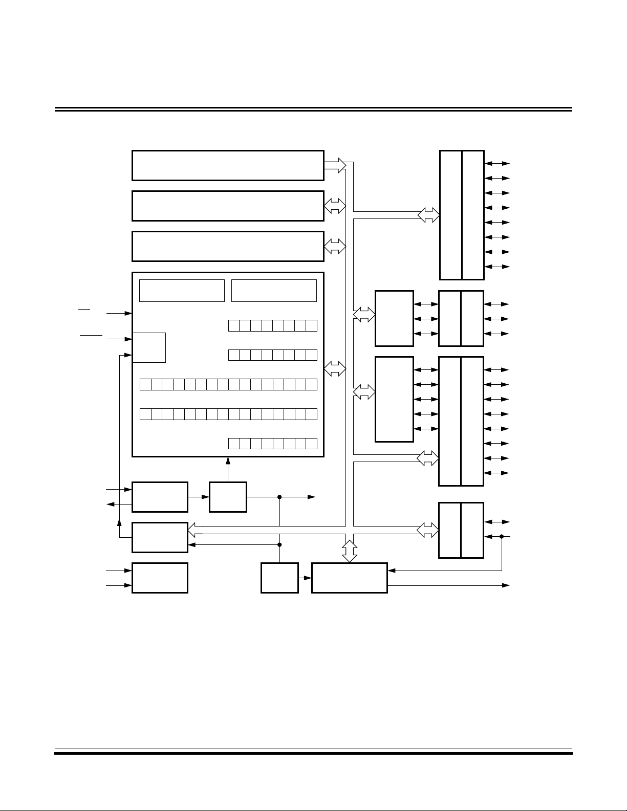
Structure
Introduction
Structure
IRQ/V
RESET
OSC1
OSC2
EPROM/OTPROM — 2104 BYTES
BOOTLOADER ROM — 240 BYTES
PORT A
RAM — 128 BYTES
DATA DIRECTION REGISTER A
CPU CONTROL
PP
RESET
00
INTERNAL
OSCILLATOR
M68HC05
MCU
STACK POINTER
0000011
000
PROGRAM COUNTER
0
ARITHMETIC/LOGIC
UNIT
ACCUMULATOR
INDEX REGISTER
CONDITION CODE REGISTER
111HINCZ
CPU CLOCK
DIVIDE
INTERNAL CLOCK
BY 2
TO ADC
AND
SIOP
SIOP
ADC
SCK
SDI
SDO
V
AN0
AN1
AN2
AN3
PORT B
REGISTER B
DA TA DIRECTION
RH
PORT C
DATA DIRECTION REGISTER C
PA7
PA6
PA5
PA4
PA3
PA2
PA1
PA0
PB7/SCK
PB6/SDI
PB5/SDO
PC7/V
RH
PC6/AN0
PC5/AN1
PC4/AN2
PC3/AN3
PC2
PC1
PC0
PD5
COP
WATCHDOG
V
DD
V
SS
POWER
DIVIDE
BY 4
CAPTURE/COMPARE
TIMER
TCAP
PORT D
REGISTER D
DA TA DIRECTION
PD7/TCAP
TCMP
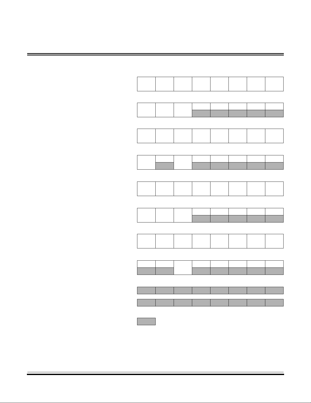
Figure 1. MC68HC705P9 Block Diagram
3-mc68hc705p9
MOTOROLA Introduction 11
Introduction
Package Types and Order Numbers
Package Types and Order Numbers
Table 1. Order Numbers
Package
Plastic DIP
SOIC
CERDIP
1. DIP = dual in-line package
2. SOIC = small outline integrated circuit
3. CERDIP = ceramic DIP
Programmable Options
Type
(2)
(3)
(1)
Case
Outline
710 28
733 28
751F 28
Count
Pin
Operating
Temperature
0 to +70 °C
–40 to +85 °C
–40 to +105 °C
–40 to +125 °C
0 to +70 °C
–40 to +85 °C
–40 to +105 °C
–40 to +125 °C
0 to +70 °C
–40 to +85 °C
–40 to +105 °C
–40 to +125 °C
Order Number
MC68HC705P9P
MC68HC705P9CP
MC68HC705P9VP
MC68HC705P9MP
MC68HC705P9DW
MC68HC705P9CDW
MC68HC705P9VDW
MC68HC705P9MDW
MC68HC705P9S
MC68HC705P9CS
MC68HC705P9VS
MC68HC705P9MS
The options in Table 2 are programmable in the mask option register.
Table 2. Programmable Options
Feature Option
Enabled
COP Watchdog
External Interrupt Pin Triggering
SIOP Data Format
12 Introduction MOTOROLA
or
Disabled
Negative-Edge Triggering Only
or
Negative-Edge and Low-Level Triggering
MSB First
or
LSB First
4-mc68hc705p9

Contents
Pin Descriptions
Pin Assignments . . . . . . . . . . . . . . . . . . . . . . . . . . . . . . . . . . . . . . . . .14
Pin Functions. . . . . . . . . . . . . . . . . . . . . . . . . . . . . . . . . . . . . . . . . . . .15
V
and VSS. . . . . . . . . . . . . . . . . . . . . . . . . . . . . . . . . . . . . . . . . . .15
DD
OSC1 and OSC2. . . . . . . . . . . . . . . . . . . . . . . . . . . . . . . . . . . . . . .15
Crystal Connections . . . . . . . . . . . . . . . . . . . . . . . . . . . . . . . . . .16
Ceramic Resonator Connections . . . . . . . . . . . . . . . . . . . . . . . .16
External Clock Connections . . . . . . . . . . . . . . . . . . . . . . . . . . . .17
RESET . . . . . . . . . . . . . . . . . . . . . . . . . . . . . . . . . . . . . . . . . . . . . .17
IRQ/VPP. . . . . . . . . . . . . . . . . . . . . . . . . . . . . . . . . . . . . . . . . . . . . .17
PA7–PA0. . . . . . . . . . . . . . . . . . . . . . . . . . . . . . . . . . . . . . . . . . . . .17
PB7/SCK–PB5/SDO . . . . . . . . . . . . . . . . . . . . . . . . . . . . . . . . . . . .17
PC7/V
PD7/TCAP and PD5 . . . . . . . . . . . . . . . . . . . . . . . . . . . . . . . . . . . .18
TCMP . . . . . . . . . . . . . . . . . . . . . . . . . . . . . . . . . . . . . . . . . . . . . . .18
–PC0 . . . . . . . . . . . . . . . . . . . . . . . . . . . . . . . . . . . . . . . . .17
RH
1-mc68hc705p9
MOTOROLA Pin Descriptions 13
Pin Descriptions
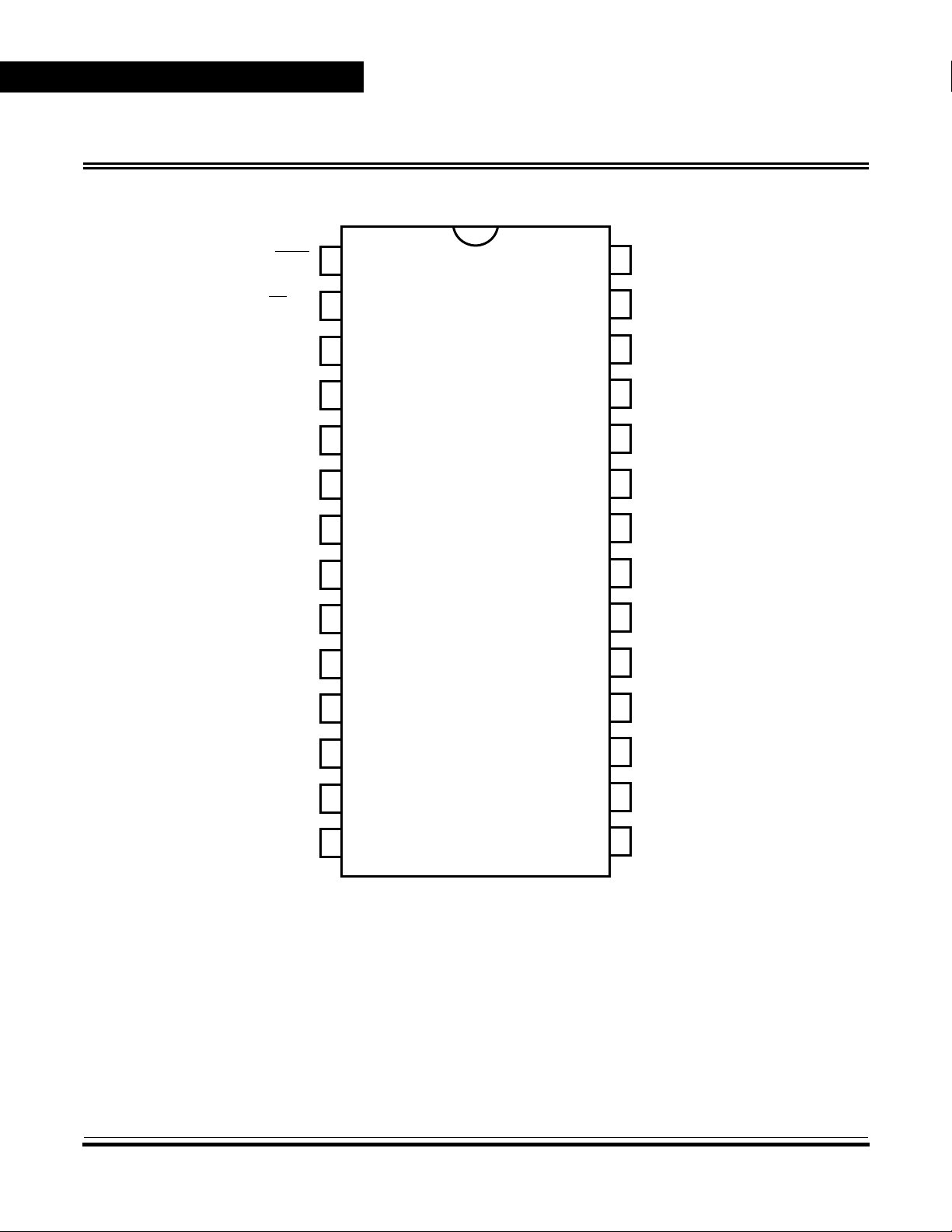
Pin Assignments
Pin Assignments
RESET
IRQ/V
PA7
PA6
PA5
PA4
PA3
PA2
PA1
PA0
PB5/SDO
V
DD
PP
OSC1
OSC2
PD7/TCAP
TCMP
PD5
PC0
PC1
PC2
PC3/AN3
PC4/AN2
PB6/SDI
PB7/SCK
V
SS
PC5/AN1
PC6/AN0
PC7/V
RH
Figure 1. Pin Assignments
2-mc68hc705p9
14 Pin Descriptions MOTOROLA
Pin Functions
Pin Descriptions
Pin Functions
VDD and V
SS
VDD and VSSare the power supply and ground pins. The MCU operates
from a single 5-V power supply.
Very fast signal transitions occur
on the MCU pins, placing high
short-duration current demands
MCU
on the power supply. To prevent
noise problems, take special
care to provide good power
DD
V
C1
0.1 µF
SS
V
supply bypassing at the MCU as
Figure 2 shows. Place the
bypass capacitors as close as
possible to the MCU. C2 is an
V
DD
C2
+
optional bulk current bypass
capacitor for use in applications
that require the port pins to
Figure 2. Bypassing
Recommendation
source high current levels.
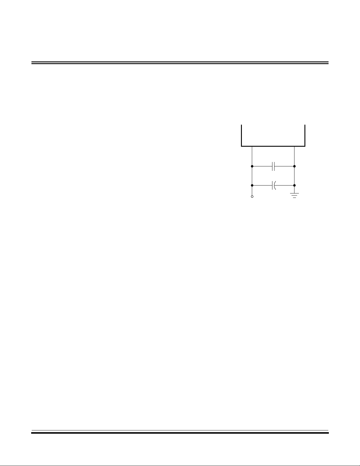
OSC1 and OSC2 The OSC1 and OSC2 pins are the connections for the on-chip oscillator.
The oscillator can be driven by any of the following:
• Crystal
• Ceramic resonator
• External clock signal
The frequency of the on-chip oscillator is f
. The MCU divides the
OSC
internal oscillator output by two to produce the internal clock with a
frequency of f
3-mc68hc705p9
OP
.
MOTOROLA Pin Descriptions 15
Pin Descriptions
Pin Functions
Crystal Connections
NOTE:
The circuit in Figure 3 shows a
typical crystal oscillator circuit
MCU
for an AT-cut, parallel resonant
crystal. Follow the crystal
supplier’s recommendations, as
OSC1
10 MΩ
OSC2
the crystal parameters
determine the external
XTAL
component values required to
provide reliable startup and
maximum stability. The load
27 pF 27 pF
capacitance values used in the
oscillator circuit design should
include all stray layout
Figure 3. Crystal Connections
capacitances. To minimize
output distortion, mount the
crystal and capacitors as close
as possible to the pins.
Use an AT-cut crystal. Do not use a strip or tuning fork crystal. The MCU
may overdrive or have the incorrect characteristic impedance for a strip
or tuning fork crystal.
Ceramic Resonator Connections
To reduce cost, use a ceramic
resonator in place of the crystal.
Figure 4 shows a ceramic
resonator circuit. For the values
of any external components,
follow the recommendations of
the resonator manufacturer. The
load capacitance values used in
the oscillator circuit design
should include all stray layout
capacitances. To minimize
output distortion, mount the
resonator and capacitors as
close as possible to the pins.
MCU
CERAMIC
RESONATOR
OSC1
OSC2
Figure 4. Ceramic Resonator
Connections
4-mc68hc705p9
16 Pin Descriptions MOTOROLA
Pin Descriptions
Pin Functions
NOTE:
Because the frequency stability of ceramic resonators is not as high as
that of crystal oscillators, using a ceramic resonator may degrade the
performance of the ADC.
External Clock Connections
An external clock from another
CMOS-compatible device can
drive the OSC1 input, with the
OSC2 pin unconnected, as
Figure 5 shows.
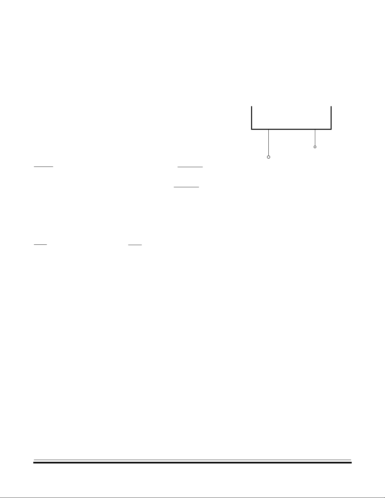
RESET A logic zero on the RESET pin
forces the MCU to a known
startup state. The
RESET pin
input circuit contains an internal
Schmitt trigger to improve noise
immunity.
MCU
OSC1
UNCONNECTED
EXTERNAL
CMOS CLOCK
OSC2
Figure 5. External Clock
Connections
IRQ/V
PP
The IRQ/VPP pin has the following functions:
• Applying asynchronous external interrupt signals
• Applying VPP, the EPROM/OTPROM programming voltage
PA7–PA0 PA7–PA0 are general-purpose bidirectional I/O port pins. Use data
direction register A to configure port A pins as inputs or outputs.
PB7/SCK– PB5/SDO
Port B is a 3-pin bidirectional I/O port that shares its pins with the SIOP.
Use data direction register B to configure port B pins as inputs or
outputs.
PC7/VRH–PC0 Port C is an 8-pin bidirectional I/O port that shares five of its pins with the
ADC. Use data direction register C to configure port C pins as inputs or
outputs.
5-mc68hc705p9
MOTOROLA Pin Descriptions 17

Pin Descriptions
Pin Functions
PD7/TCAP and PD5 Port D is a 2-pin I/O port that shares one of its pins with the
capture/compare timer. Use data direction register D to configure port D
pins as inputs or outputs.
TCMP The TCMP pin is the output compare pin for the capture/compare timer.
6-mc68hc705p9
18 Pin Descriptions MOTOROLA

Contents
Memory
Features . . . . . . . . . . . . . . . . . . . . . . . . . . . . . . . . . . . . . . . . . . . . . . .19
Memory Map . . . . . . . . . . . . . . . . . . . . . . . . . . . . . . . . . . . . . . . . . . . .20
Input/Output Register Summary . . . . . . . . . . . . . . . . . . . . . . . . . . . . .21
RAM. . . . . . . . . . . . . . . . . . . . . . . . . . . . . . . . . . . . . . . . . . . . . . . . . . .24
EPROM/OTPROM. . . . . . . . . . . . . . . . . . . . . . . . . . . . . . . . . . . . . . . .25
EPROM/OTPROM Programming . . . . . . . . . . . . . . . . . . . . . . . . . .26
EPROM Programming Register . . . . . . . . . . . . . . . . . . . . . . . . .26
Bootloader ROM . . . . . . . . . . . . . . . . . . . . . . . . . . . . . . . . . . . .27
EPROM Erasing . . . . . . . . . . . . . . . . . . . . . . . . . . . . . . . . . . . . . . .30
Mask Option Register . . . . . . . . . . . . . . . . . . . . . . . . . . . . . . . . . . . . .31
Features
1-mc68hc705p9
• 2104 Bytes of EPROM/OTPROM
– 48 Bytes of Page Zero EPROM/OTPROM
– Eight Locations for User Vectors
• 128 Bytes of User RAM
• Bootloader ROM
MOTOROLA Memory 19
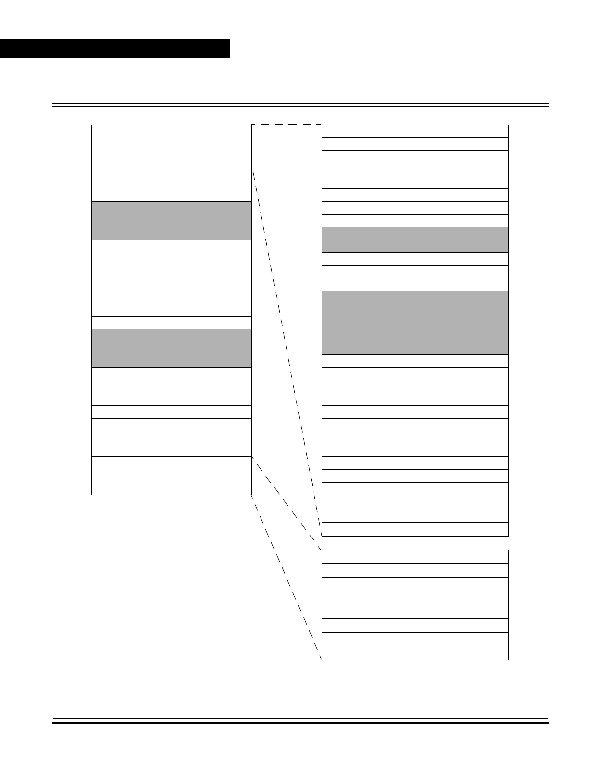
Memory Map
Memory
Memory Map
$0000
↓
$001F
$0020
↓
$004F
$0050
↓
$007F
$0080
↓
$00FF
$0100
↓
$08FF
$0900 Mask Option Register $000F
$0901
↓
$1EFF
$1F00
↓
$1FEF
$1FF0 COP Control Register Output Compare Register High (OCRH) $0016
$1FF1
↓
$1FF7
$1FF8
↓
$1FFF
I/O Registers (32 Bytes)
Page Zero User EPROM (48 Bytes)
Unimplemented (48 Bytes)
RAM (128 Bytes)
User EPROM (2048 Bytes)
Unimplemented (5631 Bytes)
Bootloader ROM (240 Bytes)
Reserved
User Vector EPROM (8 Bytes)
Port A Data Register (PORTA) $0000
Port B Data Register (PORTB) $0001
Port C Data Register (PORTC) $0002
Port D Data Register (PORTD) $0003
Data Direction Register A (DDRA) $0004
Data Direction Register B (DDRB) $0005
Data Direction Register C (DDRC) $0006
Data Direction Register D (DDRD) $0007
Unimplemented
SIOP Control Register (SCR) $000A
SIOP Status Register (SSR) $000B
SIOP Data Register (SDR) $000C
Unimplemented
Timer Control Register (TCR) $0012
Timer Status Register (TSR) $0013
Input Capture Register High (ICRH) $0014
Input Capture Register Low (ICRL) $0015
Output Compare Register Low (OCRL) $0017
Timer Register High (TRH) $0018
Timer Register Low (TRL) $0019
Alternate Timer Register High (ATRH) $001A
Alternate Timer Register Low (ATRL) $001B
EPROM Programming Register (EPROG) $001C
ADC Data Register (ADDR) $001D
ADC Status/Control Register (ADSCR) $001E
Reserved $001F
$0008
$0009
$000D
$000E
$0010
$0011
Timer Interrupt Vector High $1FF8
Timer Interrupt Vector Low $1FF9
External Interrupt Vector High $1FFA
External Interrupt Vector Low $1FFB
Software Interrupt Vector High $1FFC
Software Interrupt Vector Low $1FFD
Reset Vector High $1FFE
Reset Vector Low $1FFF
Figure 1. Memory Map
2-mc68hc705p9
20 Memory MOTOROLA
Memory
Input/Output Register Summary
Input/Output Register Summary
Addr. Name R/W Bit 7 654321Bit 0
$0000
Port A Data Register (PORTA)
Read:
Write:
Reset:
PA7 PA6 PA5 PA4 PA3 PA2 PA1 PA0
Unaffected by reset
$0001
$0002
$0003
$0004
$0005
$0006
Port B Data Register (PORTB)
Port C Data Register (PORTC)
Port D Data Register (PORTD)
Data Direction Register A (DDRA)
Data Direction Register B (DDRB)
Data Direction Register C (DDRC)
Read:
Write:
PB7 PB6 PB5
Reset:
Read:
Write:
PC7 PC6 PC5 PC4 PC3 PC2 PC1 PC0
Reset:
Read:
Write:
PD7
0
PD5
Reset:
Read:
DDRA7 DDRA6 DDRA5 DDRA4 DDRA3 DDRA2 DDRA1 DDRA0
Write:
Reset:
Read:
Write:
Reset:
Read:
Write:
Reset:
00000000
DDRB7 DDRB6 DDRB5
00000000
DDRC7 DDRC6 DDRC5 DDRC4 DDRC3 DDRC2 DDRC1 DDRC0
00000000
00000
Unaffected by reset
Unaffected by reset
10000
Unaffected by reset
00000
$0007
$0008
$0009
Data Direction Register D (DDRD)
Unimplemented
Unimplemented
Read:
Write:
Reset:
00
00000000
= Unimplemented
DDRD5
00000
= Reserved U = Unaffected
R
Figure 2. I/O Register Summary
3-mc68hc705p9
MOTOROLA Memory 21
Memory
Input/Output Register Summary
Addr. Name R/W Bit 7 654321Bit 0
$000A
SIOP Control Register (SCR)
Read:
Write:
Reset:
0 SPE 0 MSTR 0000
00000000
$000B
$000C
$000D
$000E
$000F
$0010
$0011
$0012
$0013
SIOP Status Register (SSR)
SIOP Data Register (SDR)
Unimplemented
Unimplemented
Unimplemented
Unimplemented
Unimplemented
Timer Control Register (TCR)
Timer Status Register (TSR)
Read:
Write:
Reset:
Read:
Write:
Reset:
Read:
Write:
Reset:
Read:
Write:
Reset:
SPIF DCOL 000000
00000000
Bit 7 654321Bit 0
Unaffected by reset
ICIE OCIE TOIE 0 0 0 IEDG OLVL
000000U0
ICFOCFTOF00000
Unaffected by reset 00000
$0014
Input Capture Register High (ICRH)
Read:
Write:
Bit 15 14 13 12 11 10 9 Bit 8
Reset:
$0015
$0016
Input Capture Register Low (ICRL)
Output Compare Register High (OCRH)
Read:
Write:
Reset:
Read:
Write:
Reset:
Bit 7 654321Bit 0
Unaffected by reset
Bit 15 14 13 12 11 10 9 Bit 8
Unaffected by reset
= Unimplemented
= Reserved U = Unaffected
R
Figure 2. I/O Register Summary (Continued)
4-mc68hc705p9
22 Memory MOTOROLA
Memory
Input/Output Register Summary
Addr. Name R/W Bit 7 654321Bit 0
$0017
Output Compare Register Low (OCRL)
Read:
Write:
Reset:
Bit 7 654321Bit 0
Unaffected by reset
$0018
$0019
$001A
$001B
$001C
$001D
Timer Register High (TRH)
Timer Register Low (TRL)
Alternate Timer Register High (ATRH)
Alternate Timer Register Low (ATRL)
EPROMProgramming Register (EPROG)
ADC Data Register (ADDR)
Read:
Write:
Reset:
Read:
Write:
Reset:
Read:
Write:
Reset:
Read:
Write:
Reset:
Read:
Write:
Reset:
Read:
Write:
Reset:
Bit 15 14 13 12 11 10 9 Bit 8
Reset initializes TRH to $FF
Bit 7 654321Bit 0
Reset initializes TRL to $FC
Bit 15 14 13 12 11 10 9 Bit 8
Reset initializes ATRH to $FF
Bit 7 654321Bit 0
Reset initializes ATRL to $FC
00000
RRRRR R
Unaffected by reset
Bit 7 654321Bit 0
Unaffected by reset
LATCH
0
EPGM
$001E
$001F
ADC Status/Control Register (ADSCR)
Reserved
Read:
Write:
Reset:
Read:
Write:
CCF
ADRC ADON
00000000
RRRRRRRR
00
CH2 CH1 CH0
Reset:
= Unimplemented
= Reserved U = Unaffected
R
Figure 2. I/O Register Summary (Continued)
5-mc68hc705p9
MOTOROLA Memory 23
Memory
Addr. Name R/W Bit 7 654321Bit 0
RAM
$0900
$1FF0
RAM
Mask Option Register (MOR)
COP Register (COPR)
Figure 2. I/O Register Summary (Continued)
The 128 addresses from $0080–$00FF are RAM locations. The CPU
uses the top 64 RAM addresses, $00C0–$00FF, as the stack. Before
processing an interrupt, the CPU uses five bytes of the stack to save the
contents of the CPU registers. During a subroutine call, the CPU uses
two bytes of the stack to store the return address. The stack pointer
decrements when the CPU stores a byte on the stack and increments
when the CPU retrieves a byte from the stack.
Read:
Write:
Reset:
Read:
Write:
Reset:
00000SIOP IRQ COPE
Unaffected by reset 0
RRRRRRRCOPC
Unaffected by reset
= Unimplemented
= Reserved U = Unaffected
R
NOTE:
Be careful when using nested subroutines or multiple interrupt levels.
The CPU may overwrite data in the RAM during a subroutine or during
the interrupt stacking operation.
6-mc68hc705p9
24 Memory MOTOROLA

EPROM/OTPROM
Memory
EPROM/OTPROM
An MCU with a quartz window has 2104 bytes of erasable,
programmable ROM (EPROM). The quartz window allows EPROM
erasure with ultraviolet light.
NOTE:
Keep the quartz window covered with an opaque material except when
programming the MCU. Ambient light may affect MCU operation.
In an MCU without the quartz window, the EPROM cannot be erased
and serves as 2104 bytes of one-time programmable ROM (OTPROM).
The following addresses are user EPROM/OTPROM locations:
• $0020–$004F
• $0100–$08FF
• $1FF8–$1FFF (reserved for user-defined interrupt and reset
vectors)
The mask option register (MOR) is an EPROM/OTPROM location at
address $0900.
7-mc68hc705p9
MOTOROLA Memory 25

Memory
EPROM/OTPROM
EPROM/ OTPROM Programming
EPROM Programming Register
The two ways to program the EPROM/OTPROM are:
• Manipulating the control bits in the EPROM programming register
to program the EPROM/OTPROM on a byte-by-byte basis
• Activating the bootloader ROM to download the contents of an
external memory device to the on-chip EPROM/OTPROM
The EPROM programming register contains the control bits for
programming the EPROM/OTPROM.
$001C Bit 7 654321Bit 0
Read: 00000
LATCH
Write: RRRRR R
Reset: 00000000
R = Reserved
0
EPGM
Figure 3. EPROM Programming Register (EPROG)
LATCH — EPROM Bus Latch
This read/write bit latches the address and data buses for
EPROM/OTPROM programming. Clearing the LATCH bit
automatically clears the EPGM bit. EPROM/OTPROM data cannot be
read while the LATCH bit is set. Resets clear the LATCH bit.
1 = Address and data buses configured for EPROM/OTPROM
programming
0 = Address and data buses configured for normal operation
EPGM bit— EPROM Programming
This read/write bit applies the voltage from the
IRQ/VPP pin to the
EPROM/OTPROM. To write the EPGM bit, the LATCH bit must
already be set. Clearing the LATCH bit also clears the EPGM bit.
Resets clear the EPGM bit.
1 = EPROM/OTPROM programming power switched on
0 = EPROM/OTPROM programming power switched off
8-mc68hc705p9
26 Memory MOTOROLA

Memory
EPROM/OTPROM
NOTE:
Writing logic ones to both the LATCH and EPGM bits with a single
instruction sets LATCH and clears EPGM. LATCH must be set first by a
separate instruction.
Bits 7–3 and Bit 1— Reserved
Bits 7–3 and bit 1 are factory test bits that always read as logic zeros.
Take the following steps to program a byte of EPROM/OTPROM:
1. Apply 16.5 V to the
IRQ/VPP pin.
2. Set the LATCH bit.
3. Write to any EPROM/OTPROM address.
4. Set the EPGM bit for a time, t
, to apply the programming
EPGM
voltage.
5. Clear the LATCH bit.
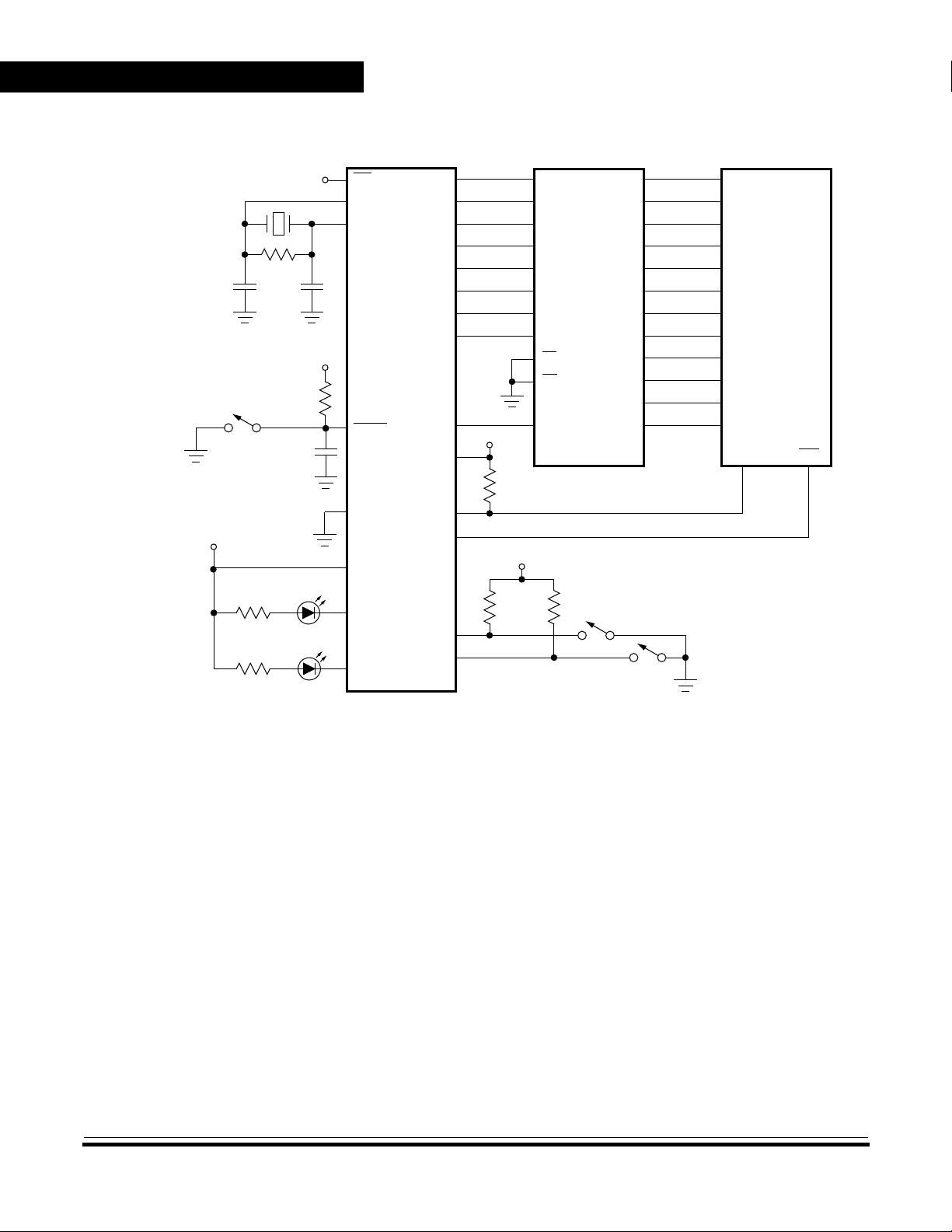
Bootloader ROM The bootloader ROM, located at addresses $1F00–$1FEF, contains
routines for copying an external EPROM to the on-chip
EPROM/OTPROM.
The bootloader copies to the following EPROM/OTPROM addresses:
• $0020–$004F
• $0100–$0900
• $1FF0–$1FFF
The addresses of the code in the external EPROM must match the
MC68HC705P9 addresses. The bootloader ignores all other addresses.
Figure 4 shows the circuit for downloading to the on-chip
EPROM/OTPROM from a 2764 EPROM. The bootloader circuit includes
an external 12-bit counter to address the external EPROM. Operation is
fastest when unused external EPROM addresses contain $00. The
bootloader function begins when a rising edge occurs on the
while the V
voltage is on the IRQ/VPP pin, and the PD7/TCAP pin is at
PP
RESETpin
logic one.
9-mc68hc705p9
MOTOROLA Memory 27
Memory
EPROM/OTPROM
MC14040B
Q1
Q2
Q3
Q4
Q5
Q6
Q7
Q8
Q9
Q10
Q11
Q12
RST CLK
S1
2 MHz
10 MΩ
10 kΩ
1 µF
D0
D1
D2
D3
D4
D5
D6
D7
CE
OE
2764
A0
A1
A2
A3
A4
A5
A6
A7
A8
A9
MC68HC705P9
2
V
IRQ/V
PP
27
26
V
DD
PP
OSC1
OSC2
PA0
PA1
PA2
PA3
PA4
PA5
PA6
PA7
10
9
8
7
6
5
4
3
A10
1
RESET
PB5
PD7
11
25
A12
V
DD
A11
10 kΩ
17
PC5/AN1
V
DD
16
PC6/AN0
PC1
PC2
21
20
V
DD
PROGRAM
330 Ω
VERIFY
13
12
PB7/SCK
PB6/SDI
PC4
PC3
10 kΩ
18
19
10 kΩ
S2
S3
330 Ω
Figure 4. Bootloader Circuit
10-mc68hc705p9
28 Memory MOTOROLA
EPROM/OTPROM
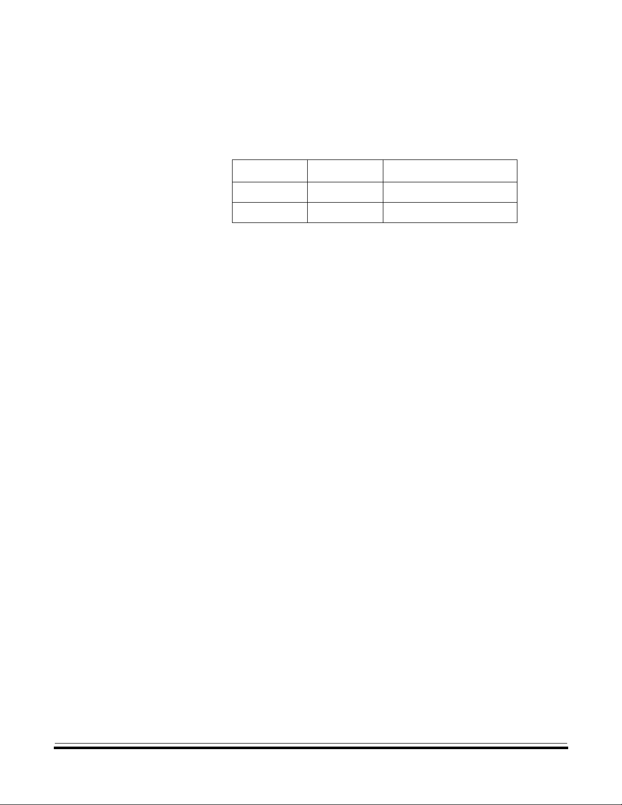
The logical states of the PC4/AN2 and PC3/AN3 pins select the
bootloader function, as Table 1 shows.
Table 1. Bootloader Function Selection
Memory
PC4/AN2 PC3/AN3
1 1 Program and Verify
1 0 Verify Only
Function
Complete the following steps to bootload the MCU:
1. Turn off all power to the circuit.
2. Install the EPROM containing the code to be downloaded.
3. Install the MCU.
4. Select the bootloader function:
a. Open switches S2 and S3 to select the program and verify
function.
b. Open only switch S2 to select only the verify function.
5. Close switch S1.
6. Turn on the V
power supply.
DD
CAUTION:
Turn on the VDD power supply before turning on the VPP power supply.
7. Turn on the VPP power supply.
8. Open switch S1. The bootloader code begins to execute. If the
PROGRAM function is selected, the PROGRAM LED turns on
during programming. If the VERIFY function is selected, the
VERIFY LED turns on when verification is successful. The
PROGRAM and VERIFY functions take about 10 seconds.
9. Close switch S1.
10. Turn off the V
11-mc68hc705p9
MOTOROLA Memory 29
power supply.
PP

Memory
EPROM/OTPROM
CAUTION:
Turn off the VPP power supply before turning off the VDD power supply.
11. Turn off the VDD power supply.
EPROM Erasing The erased state of an EPROM bit is zero. Erase the EPROM by
exposing it to 15 Ws/cm
2
of ultraviolet light with a wavelength of 2537
angstroms. Position the ultraviolet light source one inch from the
EPROM. Do not use a shortwave filter.
Cerdip packages have a transparent window for erasing the EPROM
with ultraviolet light. In the windowless PDIP and SOIC packages, the
2104 EPROM bytes function as one-time programmable ROM
(OTPROM).
12-mc68hc705p9
30 Memory MOTOROLA
 Loading...