

Motorola MC68HC705J1AVS, MC68HC705J1AS, MC68HC705J1AP, MC68HC705J1ACS, MC68HC705J1AC Datasheet
...
M68HC05
Microcontrollers
MC68HC705J1A
MC68HRC705J1A
MC68HSC705J1A
MC68HSR705J1A
Technical Data
MC68HC705J1A/D
Rev. 4, 5/2002
WWW.MOTOROLA.COM/SEMICONDUCTORS


MC68HC705J1A
MC68HRC705J1A
MC68HSC705J1A
MC68HSR705J1A
Technical Data
To provide the most up-to-date information, the revision of our
documents on the World Wide Web will be the most current. Your printed
copy may b e an earlier revision. To ve rify you have the latest information
available, refer to:
http://www.motorola.com/semiconductors/
The following revision history table summarizes changes contained in
this document. For your convenience, the page number designators
have been linked to the appropriate location.
Motorola and the Stylized M Logo are register ed trademarks of Motorola, Inc.
digital dna is a trademark of Motorola, Inc. © Motorola, Inc., 2002
MC68HC705J1A — Rev. 4.0 Technical Data
MOTOROLA 3

Technical Data
Revision History
Date
May , 2002 4.0
Revision
Level
Description
Figure 2-2. I/O Register Summary — Corrected reset state for
last entry (Mask Option Register)
Figure 2-4. Mask Option Register (MOR) — Corrected reset
state
6.3.3 Pulldown Register A — Corrected note 91
6.4.3 Pulldown Register B — Corrected note 94
Page
Number(s)
37
41
Technical Data MC68HC705J1A — Rev. 4.0
4 MOTOROLA

Technical Data — MC68HC705J1A
Section 1. General Description . . . . . . . . . . . . . . . . . . . .21
Section 2. Memory . . . . . . . . . . . . . . . . . . . . . . . . . . . . . .33
Section 3. Central Processor Unit (CPU) . . . . . . . . . . . .45
Section 4. Resets and Interrupts . . . . . . . . . . . . . . . . . . .69
Section 5. Low-Power Modes. . . . . . . . . . . . . . . . . . . . . .79
Section 6. Parallel Input/Output (I/O) Ports . . . . . . . . . .87
Section 7. Computer Oper at in g Pro pe rl y
List of Sections
(COP) Module . . . . . . . . . . . . . . . . . . . . . . . . .97
Section 8. External Interrupt Module (IRQ). . . . . . . . . .101
Section 9. Multifunction Timer Module . . . . . . . . . . . . .109
Section 10. Electrical Specifications. . . . . . . . . . . . . . .117
Section 11. Mechanical Specifications . . . . . . . . . . . . .131
Section 12. Ordering Information . . . . . . . . . . . . . . . . .135
Appendix A. MC68HRC705J1A . . . . . . . . . . . . . . . . . . .137
Appendix B. MC68HSC705J1A . . . . . . . . . . . . . . . . . . .141
Appendix C. MC68HSR705J1A . . . . . . . . . . . . . . . . . . .145
Index. . . . . . . . . . . . . . . . . . . . . . . . . . . . . . . . . . . . . . . . 151
MC68HC705J1A — Rev . 4.0 Technical Data
MOTOROLA List of Sections 5

List of Sec ti o ns
Technical Data MC68HC705J1A — Rev. 4.0
6 List of Sections MOTOROLA

Technical Data — MC68HC705J1A
Section 1. General Description
1.1 Contents. . . . . . . . . . . . . . . . . . . . . . . . . . . . . . . . . . . . . . . . . .21
1.2 Introduction. . . . . . . . . . . . . . . . . . . . . . . . . . . . . . . . . . . . . . . .22
1.3 Features . . . . . . . . . . . . . . . . . . . . . . . . . . . . . . . . . . . . . . . . . .24
1.4 Programmable Options. . . . . . . . . . . . . . . . . . . . . . . . . . . . . . .25
1.5 Pin Assignments. . . . . . . . . . . . . . . . . . . . . . . . . . . . . . . . . . . .25
1.5.1 V
1.5.2 OSC1 and OSC2 . . . . . . . . . . . . . . . . . . . . . . . . . . . . . . . . . 2 7
1.5.2.1 Crystal Oscillator . . . . . . . . . . . . . . . . . . . . . . . . . . . . . . .27
1.5.2.2 Ceramic Resonator Oscillator . . . . . . . . . . . . . . . . . . . . .28
1.5.2.3 RC Oscillator . . . . . . . . . . . . . . . . . . . . . . . . . . . . . . . . . .30
1.5.2.4 External Clock . . . . . . . . . . . . . . . . . . . . . . . . . . . . . . . . .30
and VSS. . . . . . . . . . . . . . . . . . . . . . . . . . . . . . . . . . . . .25
DD
Table of Contents
1.6 RESET . . . . . . . . . . . . . . . . . . . . . . . . . . . . . . . . . . . . . . . . . . .30
1.7 IRQ/VPP . . . . . . . . . . . . . . . . . . . . . . . . . . . . . . . . . . . . . . . . . .31
1.8 PA0–PA7 . . . . . . . . . . . . . . . . . . . . . . . . . . . . . . . . . . . . . . . . .31
1.9 PB0–PB5 . . . . . . . . . . . . . . . . . . . . . . . . . . . . . . . . . . . . . . . . .31
Section 2. M em o ry
2.1 Contents. . . . . . . . . . . . . . . . . . . . . . . . . . . . . . . . . . . . . . . . . .33
2.2 Introduction. . . . . . . . . . . . . . . . . . . . . . . . . . . . . . . . . . . . . . . .33
2.3 Memory Map. . . . . . . . . . . . . . . . . . . . . . . . . . . . . . . . . . . . . . .34
2.4 Input/Output Register Summary. . . . . . . . . . . . . . . . . . . . . . . .35
2.5 RAM . . . . . . . . . . . . . . . . . . . . . . . . . . . . . . . . . . . . . . . . . . . . .37
MC68HC705J1A — Rev . 4.0 Technical Data
MOTOROLA Table of Contents 7

Table of Contents
2.6 EPROM/OTPROM . . . . . . . . . . . . . . . . . . . . . . . . . . . . . . . . . .38
2.6.1 EPROM/OTPROM Programming. . . . . . . . . . . . . . . . . . . . .38
2.6.2 EPROM Programming Register . . . . . . . . . . . . . . . . . . . . .39
2.6.3 EPROM Erasing. . . . . . . . . . . . . . . . . . . . . . . . . . . . . . . . . .40
2.7 Mask Option Register. . . . . . . . . . . . . . . . . . . . . . . . . . . . . . . .40
2.8 EPROM Programming Characteristics. . . . . . . . . . . . . . . . . . .43
Section 3. Central Processor Unit (CPU)
3.1 Contents. . . . . . . . . . . . . . . . . . . . . . . . . . . . . . . . . . . . . . . . . .45
3.2 Introduction. . . . . . . . . . . . . . . . . . . . . . . . . . . . . . . . . . . . . . . .46
3.3 CPU Control Unit . . . . . . . . . . . . . . . . . . . . . . . . . . . . . . . . . . .46
3.4 Arithmetic/Logic Unit. . . . . . . . . . . . . . . . . . . . . . . . . . . . . . . . .46
3.5 CPU Registers . . . . . . . . . . . . . . . . . . . . . . . . . . . . . . . . . . . . .48
3.5.1 Accumulator . . . . . . . . . . . . . . . . . . . . . . . . . . . . . . . . . . . . .48
3.5.2 Index Register . . . . . . . . . . . . . . . . . . . . . . . . . . . . . . . . . . .48
3.5.3 Stack Pointer . . . . . . . . . . . . . . . . . . . . . . . . . . . . . . . . . . . .49
3.5.4 Program Counter . . . . . . . . . . . . . . . . . . . . . . . . . . . . . . . . .50
3.5.5 Condition Code Register . . . . . . . . . . . . . . . . . . . . . . . . . . .50
3.6 Instruction Set. . . . . . . . . . . . . . . . . . . . . . . . . . . . . . . . . . . . . .52
3.6.1 Addressing Modes . . . . . . . . . . . . . . . . . . . . . . . . . . . . . . . .52
3.6.1.1 Inherent . . . . . . . . . . . . . . . . . . . . . . . . . . . . . . . . . . . . . .52
3.6.1.2 Immediate . . . . . . . . . . . . . . . . . . . . . . . . . . . . . . . . . . . .52
3.6.1.3 Direct . . . . . . . . . . . . . . . . . . . . . . . . . . . . . . . . . . . . . . . .53
3.6.1.4 Extended . . . . . . . . . . . . . . . . . . . . . . . . . . . . . . . . . . . . .53
3.6.1.5 Indexed, No Offset. . . . . . . . . . . . . . . . . . . . . . . . . . . . . .53
3.6.1.6 Indexed, 8-Bit Offset . . . . . . . . . . . . . . . . . . . . . . . . . . . .53
3.6.1.7 Indexed, 16-Bit Offset . . . . . . . . . . . . . . . . . . . . . . . . . . .54
3.6.1.8 Relative . . . . . . . . . . . . . . . . . . . . . . . . . . . . . . . . . . . . . .54
3.6.2 Instruction Types . . . . . . . . . . . . . . . . . . . . . . . . . . . . . . . . .55
3.6.2.1 Register/Memory Instructions . . . . . . . . . . . . . . . . . . . . .55
3.6.2.2 Read-Modify-Write Instructions . . . . . . . . . . . . . . . . . . . .56
3.6.2.3 Jump/Branch Instructions . . . . . . . . . . . . . . . . . . . . . . . .57
3.6.2.4 Bit Manipulation Instructions . . . . . . . . . . . . . . . . . . . . . .59
3.6.2.5 Control Instructions . . . . . . . . . . . . . . . . . . . . . . . . . . . . .60
Technical Data MC68HC705J1A — Rev. 4.0
8 Table of Contents M OTOROLA

Table of Contents
3.7 Instruction Set Summary . . . . . . . . . . . . . . . . . . . . . . . . . . . . .61
3.8 Opcode Map. . . . . . . . . . . . . . . . . . . . . . . . . . . . . . . . . . . . . . .66
Section 4. Resets and In ter r upts
4.1 Contents. . . . . . . . . . . . . . . . . . . . . . . . . . . . . . . . . . . . . . . . . .69
4.2 Introduction. . . . . . . . . . . . . . . . . . . . . . . . . . . . . . . . . . . . . . . .69
4.3 Resets. . . . . . . . . . . . . . . . . . . . . . . . . . . . . . . . . . . . . . . . . . . .70
4.3.1 Power-On Reset. . . . . . . . . . . . . . . . . . . . . . . . . . . . . . . . . .71
4.3.2 External Reset . . . . . . . . . . . . . . . . . . . . . . . . . . . . . . . . . . .72
4.3.3 COP Watchdog Reset . . . . . . . . . . . . . . . . . . . . . . . . . . . . .72
4.3.4 Illegal Address Reset . . . . . . . . . . . . . . . . . . . . . . . . . . . . . .72
4.4 Interrupts. . . . . . . . . . . . . . . . . . . . . . . . . . . . . . . . . . . . . . . . . .73
4.4.1 Software Interrupt. . . . . . . . . . . . . . . . . . . . . . . . . . . . . . . . .73
4.4.2 External Interrupt . . . . . . . . . . . . . . . . . . . . . . . . . . . . . . . . .73
4.4.3 Timer Interrupts . . . . . . . . . . . . . . . . . . . . . . . . . . . . . . . . . .76
4.4.3.1 Real-Time Interrupt . . . . . . . . . . . . . . . . . . . . . . . . . . . . .7 6
4.4.3.2 Timer Overflow Interrupt . . . . . . . . . . . . . . . . . . . . . . . . .76
4.4.4 Interrupt Processing. . . . . . . . . . . . . . . . . . . . . . . . . . . . . . .76
Section 5. Low-Power Modes
5.1 Contents. . . . . . . . . . . . . . . . . . . . . . . . . . . . . . . . . . . . . . . . . .79
5.2 Introduction. . . . . . . . . . . . . . . . . . . . . . . . . . . . . . . . . . . . . . . .79
5.3 Exiting Stop and Wait Modes . . . . . . . . . . . . . . . . . . . . . . . . . .80
5.4 Effects of Stop and Wait Modes . . . . . . . . . . . . . . . . . . . . . . . .81
5.4.1 Clock Generation . . . . . . . . . . . . . . . . . . . . . . . . . . . . . . . . .81
5.4.2 CPU . . . . . . . . . . . . . . . . . . . . . . . . . . . . . . . . . . . . . . . . . . .82
5.4.3 COP Watchdog . . . . . . . . . . . . . . . . . . . . . . . . . . . . . . . . . .82
5.4.4 Timer . . . . . . . . . . . . . . . . . . . . . . . . . . . . . . . . . . . . . . . . . .83
5.4.5 EPROM/OTPROM . . . . . . . . . . . . . . . . . . . . . . . . . . . . . . . .84
5.4.6 Data-Retention Mode. . . . . . . . . . . . . . . . . . . . . . . . . . . . . .84
5.5 Timing. . . . . . . . . . . . . . . . . . . . . . . . . . . . . . . . . . . . . . . . . . . .85
MC68HC705J1A — Rev. 4.0 Technical Data
MOTOROLA Table of Contents 9

Table of Contents
Section 6. Parallel Input/Output (I/O) Ports
6.1 Contents. . . . . . . . . . . . . . . . . . . . . . . . . . . . . . . . . . . . . . . . . .87
6.2 Introduction. . . . . . . . . . . . . . . . . . . . . . . . . . . . . . . . . . . . . . . .87
6.3 Port A . . . . . . . . . . . . . . . . . . . . . . . . . . . . . . . . . . . . . . . . . . . .89
6.3.1 Port A Data Register . . . . . . . . . . . . . . . . . . . . . . . . . . . . . .89
6.3.2 Data Direction Register A. . . . . . . . . . . . . . . . . . . . . . . . . . .90
6.3.3 Pulldown Register A. . . . . . . . . . . . . . . . . . . . . . . . . . . . . . .91
6.3.4 Port A LED Drive Capability. . . . . . . . . . . . . . . . . . . . . . . . .92
6.3.5 Port A I/O Pin Interrupts. . . . . . . . . . . . . . . . . . . . . . . . . . . .92
6.4 Port B . . . . . . . . . . . . . . . . . . . . . . . . . . . . . . . . . . . . . . . . . . . .92
6.4.1 Port B Data Register . . . . . . . . . . . . . . . . . . . . . . . . . . . . . .92
6.4.2 Data Direction Register B. . . . . . . . . . . . . . . . . . . . . . . . . . .93
6.4.3 Pulldown Register B. . . . . . . . . . . . . . . . . . . . . . . . . . . . . . .94
6.5 5.0-Volt I/O Port Electrical Characteristics . . . . . . . . . . . . . . . .95
6.6 3.3-Volt I/O Port Electrical Characteristics . . . . . . . . . . . . . . . .95
Section 7. Computer Operating Properly
(COP ) Module
7.1 Contents. . . . . . . . . . . . . . . . . . . . . . . . . . . . . . . . . . . . . . . . . .97
7.2 Introduction. . . . . . . . . . . . . . . . . . . . . . . . . . . . . . . . . . . . . . . .97
7.3 Operation . . . . . . . . . . . . . . . . . . . . . . . . . . . . . . . . . . . . . . . . .98
7.3.1 COP Watchdog Timeout . . . . . . . . . . . . . . . . . . . . . . . . . . .98
7.3.2 COP Watchdog Timeout Period. . . . . . . . . . . . . . . . . . . . . .98
7.3.3 Clearing the COP Watchdog . . . . . . . . . . . . . . . . . . . . . . . .98
7.4 Interrupts. . . . . . . . . . . . . . . . . . . . . . . . . . . . . . . . . . . . . . . . . .99
7.5 COP Register . . . . . . . . . . . . . . . . . . . . . . . . . . . . . . . . . . . . . .99
7.6 Low-Power Modes . . . . . . . . . . . . . . . . . . . . . . . . . . . . . . . . .100
7.6.1 Stop Mode . . . . . . . . . . . . . . . . . . . . . . . . . . . . . . . . . . . . .100
7.6.2 Wait Mode . . . . . . . . . . . . . . . . . . . . . . . . . . . . . . . . . . . . .100
Technical Data MC68HC705J1A — Rev. 4.0
10 Table of Contents M OTOROLA

Table of Contents
Section 8. External Interrupt Module (IRQ)
8.1 Contents. . . . . . . . . . . . . . . . . . . . . . . . . . . . . . . . . . . . . . . . .101
8.2 Introduction. . . . . . . . . . . . . . . . . . . . . . . . . . . . . . . . . . . . . . .101
8.3 Operation . . . . . . . . . . . . . . . . . . . . . . . . . . . . . . . . . . . . . . . .102
8.3.1 IRQ/VPP Pin . . . . . . . . . . . . . . . . . . . . . . . . . . . . . . . . . . . .104
8.3.2 Optional External Interrupts . . . . . . . . . . . . . . . . . . . . . . . .104
8.4 IRQ Status and Control Register . . . . . . . . . . . . . . . . . . . . . . 106
8.5 External Interrupt Timing . . . . . . . . . . . . . . . . . . . . . . . . . . . .107
8.5.1 5.0-Volt External Interrupt Timing Characteristics . . . . . . .107
8.5.2 3.3-Volt External Interrupt Timing Characteristics . . . . . . .107
Sectio n 9. Mu ltifunct io n Ti mer Modul e
9.1 Contents. . . . . . . . . . . . . . . . . . . . . . . . . . . . . . . . . . . . . . . . .109
9.2 Introduction. . . . . . . . . . . . . . . . . . . . . . . . . . . . . . . . . . . . . . .109
9.3 Operation . . . . . . . . . . . . . . . . . . . . . . . . . . . . . . . . . . . . . . . .111
9.4 Interrupts. . . . . . . . . . . . . . . . . . . . . . . . . . . . . . . . . . . . . . . . .112
9.5 I/O Registers. . . . . . . . . . . . . . . . . . . . . . . . . . . . . . . . . . . . . .112
9.5.1 Timer Status and Control Register. . . . . . . . . . . . . . . . . . .112
9.5.2 Timer Counter Register . . . . . . . . . . . . . . . . . . . . . . . . . . .114
9.6 Low-Power Modes . . . . . . . . . . . . . . . . . . . . . . . . . . . . . . . . .115
9.6.1 Stop Mode . . . . . . . . . . . . . . . . . . . . . . . . . . . . . . . . . . . . .115
9.6.2 Wait Mode . . . . . . . . . . . . . . . . . . . . . . . . . . . . . . . . . . . . .115
Section 10. Electrical Specifications
10.1 Contents. . . . . . . . . . . . . . . . . . . . . . . . . . . . . . . . . . . . . . . . .117
10.2 Introduction. . . . . . . . . . . . . . . . . . . . . . . . . . . . . . . . . . . . . . .117
10.3 Maximum Ratings. . . . . . . . . . . . . . . . . . . . . . . . . . . . . . . . . .118
10.4 Operating Temperature Range. . . . . . . . . . . . . . . . . . . . . . . .119
10.5 Thermal Characteristics . . . . . . . . . . . . . . . . . . . . . . . . . . . . .119
MC68HC705J1A — Rev. 4.0 Technical Data
MOTOROLA Table of Contents 11

Table of Contents
10.6 Power Considerations. . . . . . . . . . . . . . . . . . . . . . . . . . . . . . .120
10.7 5.0-Volt DC Electrical Characteristics. . . . . . . . . . . . . . . . . . .121
10.8 3.3-Volt DC Electrical Characteristics . . . . . . . . . . . . . . . . . .122
10.9 Driver Characteristics. . . . . . . . . . . . . . . . . . . . . . . . . . . . . . .123
10.10 Typical Supply Currents . . . . . . . . . . . . . . . . . . . . . . . . . . . . .125
10.11 EPROM Programming Characteristics. . . . . . . . . . . . . . . . . .126
10.12 5.0-Volt Control Timing . . . . . . . . . . . . . . . . . . . . . . . . . . . .126
10.13 3.3-Volt Control Timing . . . . . . . . . . . . . . . . . . . . . . . . . . . . .127
Section 11. Mechanical Specifications
11.1 Contents. . . . . . . . . . . . . . . . . . . . . . . . . . . . . . . . . . . . . . . . .131
11.2 Introduction. . . . . . . . . . . . . . . . . . . . . . . . . . . . . . . . . . . . . . .131
11.3 Plastic Dual In-Line Package (Case 738). . . . . . . . . . . . . . . .132
11.4 Small Outline Integrated Circuit (Case 751). . . . . . . . . . . . . .132
11.5 Ceramic Dual In-Line Package (Case 732) . . . . . . . . . . . . . . 133
Section 12. Ordering Information
12.1 Contents. . . . . . . . . . . . . . . . . . . . . . . . . . . . . . . . . . . . . . . . .135
12.2 Introduction. . . . . . . . . . . . . . . . . . . . . . . . . . . . . . . . . . . . . . .135
12.3 MCU Order Numbers . . . . . . . . . . . . . . . . . . . . . . . . . . . . . . .135
Appendix A. MC68HRC705J1A
A.1 Contents. . . . . . . . . . . . . . . . . . . . . . . . . . . . . . . . . . . . . . . . .137
A.2 Introduction. . . . . . . . . . . . . . . . . . . . . . . . . . . . . . . . . . . . . . .137
A.3 RC Oscillator Connections . . . . . . . . . . . . . . . . . . . . . . . . . . . 1 3 8
A.4 Typical Internal Operating Frequency
for RC Oscillator Option. . . . . . . . . . . . . . . . . . . . . . . . . . .139
A.5 Package Types and Order Numbers . . . . . . . . . . . . . . . . . . .140
Technical Data MC68HC705J1A — Rev. 4.0
12 Table of Contents M OTOROLA

Table of Contents
Appendix B. MC68HSC705J1A
B.1 Contents. . . . . . . . . . . . . . . . . . . . . . . . . . . . . . . . . . . . . . . . .141
B.2 Introduction. . . . . . . . . . . . . . . . . . . . . . . . . . . . . . . . . . . . . . .141
B.3 5.0-Volt DC Electrical Characteristics. . . . . . . . . . . . . . . . . . .142
B.4 3.3-Volt DC Electrical Characteristics. . . . . . . . . . . . . . . . . . .142
B.5 Typical Supply Currents . . . . . . . . . . . . . . . . . . . . . . . . . . . . .142
B.6 Package Types and Order Numbers . . . . . . . . . . . . . . . . . . .144
Appendix C. MC68HSR705J1A
C.1 Contents . . . . . . . . . . . . . . . . . . . . . . . . . . . . . . . . . . . . . . . . .145
C.2 Introduction. . . . . . . . . . . . . . . . . . . . . . . . . . . . . . . . . . . . . . .145
C.3 RC Oscillator Connections (External Resistor). . . . . . . . . . . .14 5
C.4 Typical Internal Operating Frequency at 25°C
for High-Speed RC Oscillator Option. . . . . . . . . . . . . . . . .146
C.5 RC Oscillator Connections (No External Resistor). . . . . . . . .147
C.6 Typical Internal Operating Frequency versus Temperature
(No External Resistor). . . . . . . . . . . . . . . . . . . . . . . . . . . .148
C.7 Package Types and Order Numbers . . . . . . . . . . . . . . . . . . .149
Index
Index . . . . . . . . . . . . . . . . . . . . . . . . . . . . . . . . . . . . . . . . . . .151
MC68HC705J1A — Rev. 4.0 Technical Data
MOTOROLA Table of Contents 13

Table of Contents
Technical Data MC68HC705J1A — Rev. 4.0
14 Table of Contents M OTOROLA

Technical Data — MC68HC705J1A
Figure Title P age
1-1 Block Diagram . . . . . . . . . . . . . . . . . . . . . . . . . . . . . . . . . . .23
1-2 Pin Assignments. . . . . . . . . . . . . . . . . . . . . . . . . . . . . . . . . .26
1-3 Bypassing Layout Recommendation . . . . . . . . . . . . . . . . . .26
1-4 Crystal Connections with
Oscillator Internal Resistor Mask Option. . . . . . . . . . . . .28
1-5 Crystal Connections without
Oscillator Internal Resistor Mask Option. . . . . . . . . . . . .28
1-6 Ceramic Resonator Connections
with Oscillator Internal Resistor Mask Option . . . . . . . . .29
List of Figures
1-7 Ceramic Resonator Connections
without Oscillator Internal Resistor Mask Op tion. . . . . . .29
1-8 External Clock Connections. . . . . . . . . . . . . . . . . . . . . . . . .30
2-1 Memory Map . . . . . . . . . . . . . . . . . . . . . . . . . . . . . . . . . . . .34
2-2 I/O Register Summary . . . . . . . . . . . . . . . . . . . . . . . . . . . . .35
2-3 EPROM Programming Register (EPROG). . . . . . . . . . . . . .39
2-4 Mask Option Register (MOR). . . . . . . . . . . . . . . . . . . . . . . .41
3-1 Programming Model. . . . . . . . . . . . . . . . . . . . . . . . . . . . . . .47
3-2 Accumulator (A) . . . . . . . . . . . . . . . . . . . . . . . . . . . . . . . . . .48
3-3 Index Register (X) . . . . . . . . . . . . . . . . . . . . . . . . . . . . . . . .48
3-4 Stack Pointer (SP) . . . . . . . . . . . . . . . . . . . . . . . . . . . . . . . .49
3-5 Program Counter (PC) . . . . . . . . . . . . . . . . . . . . . . . . . . . . .50
3-6 Condition Code Register (CCR). . . . . . . . . . . . . . . . . . . . . . 5 0
4-1 Reset Sources . . . . . . . . . . . . . . . . . . . . . . . . . . . . . . . . . . .70
4-2 Power-On Reset Timing. . . . . . . . . . . . . . . . . . . . . . . . . . . .71
MC68HC705J1A — Rev . 4.0 Technical Data
MOTOROLA List of Figures 15

List of Figu r e s
Figure Title P age
4-3 External Reset Timing . . . . . . . . . . . . . . . . . . . . . . . . . . . . .7 2
4-4 External Interrupt Logic . . . . . . . . . . . . . . . . . . . . . . . . . . . .74
4-5 External Interrupt Timing . . . . . . . . . . . . . . . . . . . . . . . . . .75
4-6 Interrupt Stacking Order. . . . . . . . . . . . . . . . . . . . . . . . . . . .77
4-7 Interrupt Flowchart . . . . . . . . . . . . . . . . . . . . . . . . . . . . . . . .78
5-1 Stop Mode Recovery Timing . . . . . . . . . . . . . . . . . . . . . . . . 8 5
5-2 Stop/Halt/Wait Flowchart . . . . . . . . . . . . . . . . . . . . . . . . . . .86
6-1 Parallel I/O Port Register Summary. . . . . . . . . . . . . . . . . . .8 8
6-2 Port A Data Register (PORTA). . . . . . . . . . . . . . . . . . . . . . .89
6-3 Data Direction Register A (DDRA). . . . . . . . . . . . . . . . . . . .90
6-4 Port A I/O Circuitry. . . . . . . . . . . . . . . . . . . . . . . . . . . . . . . .90
6-5 Pulldown Register A (PDRA) . . . . . . . . . . . . . . . . . . . . . . . .91
6-6 Port B Data Register (PORTB). . . . . . . . . . . . . . . . . . . . . . .92
6-7 Data Direction Register B (DDRB). . . . . . . . . . . . . . . . . . . .93
6-8 Port B I/O Circuitry. . . . . . . . . . . . . . . . . . . . . . . . . . . . . . . .93
6-9 Pulldown Register B (PDRB) . . . . . . . . . . . . . . . . . . . . . . . .94
7-1 COP Register (COPR) . . . . . . . . . . . . . . . . . . . . . . . . . . . . .99
8-1 IRQ Module Block Diagram . . . . . . . . . . . . . . . . . . . . . . . .102
8-2 Interrupt Flowchart . . . . . . . . . . . . . . . . . . . . . . . . . . . . . . .103
8-3 IRQ Status and Control Register (ISCR) . . . . . . . . . . . . . .106
8-4 External Interrupt Timing . . . . . . . . . . . . . . . . . . . . . . . . . .107
9-1 Multifunction Timer Block Diagram. . . . . . . . . . . . . . . . . . .110
9-2 I/O Register Summary . . . . . . . . . . . . . . . . . . . . . . . . . . . .111
9-3 Timer Status and Contro l Register (TSCR) . . . . . . . . . . . .112
9-4 Timer Counter Register (TCR). . . . . . . . . . . . . . . . . . . . . .114
Technical Data MC68HC705J1A — Rev. 4.0
16 List of Figures MOTOROLA

List of Figures
Figure Title P age
10-1 PA0–PA7, PB0–PB5 Typical High-Side
Driver Characteristics . . . . . . . . . . . . . . . . . . . . . . . . . .123
10-2 PA0–PA3, PB0–PB5 Typical Low-Side
Driver Characteristics . . . . . . . . . . . . . . . . . . . . . . . . . .123
10-3 PA4–PA7 Typical Low-Side Driver Characteristics . . . . . .124
10-4 Typical Operating IDD (25°C) . . . . . . . . . . . . . . . . . . . . . . .125
10-5 Typical Wait Mode IDD (25°C) . . . . . . . . . . . . . . . . . . . . . .125
10-6 External Interrupt Timing . . . . . . . . . . . . . . . . . . . . . . . . . .128
10-7 Stop Mode Recovery Timing . . . . . . . . . . . . . . . . . . . . . . .128
10-8 Power-On Reset Timing. . . . . . . . . . . . . . . . . . . . . . . . . . .129
10-9 External Reset Timing . . . . . . . . . . . . . . . . . . . . . . . . . . . .129
A-1 RC Oscillator Connections. . . . . . . . . . . . . . . . . . . . . . . . .138
A-2 Typical Internal Operating Frequency
for Various VDD at 25°C — RC Oscillator
Option Only . . . . . . . . . . . . . . . . . . . . . . . . . . . . . . . . . .139
B-1 Typical High-Speed Operating I
(25°C) . . . . . . . . . . . . .142
DD
B-2 Typical High-Speed Wait Mode IDD (25°C) . . . . . . . . . . . .143
C-1 Typical Internal Operating Frequency
at 25°C for High-Speed RC Oscillator Option. . . . . . . .146
C-2 RC Oscillator Connections (No External Resistor). . . . . . .1 47
C-3 Typical Internal Operating Frequency
versus Temperature (OSCRES Bit = 1) . . . . . . . . . . . .148
MC68HC705J1A — Rev. 4.0 Technical Data
MOTOROLA List of Figures 17

List of Figu r e s
Technical Data MC68HC705J1A — Rev. 4.0
18 List of Figures MOTOROLA

Technical Data — MC68HC705J1A
Table Title Page
1-1 Programmable Options. . . . . . . . . . . . . . . . . . . . . . . . . . . . . .25
3-1 Register/Memory Instructions. . . . . . . . . . . . . . . . . . . . . . . . .55
3-2 Read-Modify-Write Instructions . . . . . . . . . . . . . . . . . . . . . . .56
3-3 Jump and Branch Instructions . . . . . . . . . . . . . . . . . . . . . . . .58
3-4 Bit Manipulation Instructions. . . . . . . . . . . . . . . . . . . . . . . . . . 5 9
3-5 Control Instructions. . . . . . . . . . . . . . . . . . . . . . . . . . . . . . . . .60
3-6 Instruction Set Summary . . . . . . . . . . . . . . . . . . . . . . . . . . . .61
3-7 Opcode Map. . . . . . . . . . . . . . . . . . . . . . . . . . . . . . . . . . . . . .67
List of Tables
4-1 External Reset Timing . . . . . . . . . . . . . . . . . . . . . . . . . . . . . .72
4-2 External Interrupt Timing (V
4-3 External Interrupt Timing (V
= 5.0 Vdc) . . . . . . . . . . . . . . .75
DD
= 3.3 Vdc) . . . . . . . . . . . . . . .75
DD
4-4 Reset/Interrupt Vector Addresses . . . . . . . . . . . . . . . . . . . . .77
6-1 Port A Pin Operation. . . . . . . . . . . . . . . . . . . . . . . . . . . . . . . .91
6-2 Port B Pin Operation. . . . . . . . . . . . . . . . . . . . . . . . . . . . . . . .94
9-1 Real-Time Interrupt Rate Selection . . . . . . . . . . . . . . . . . . .114
12-1 Order Numbers. . . . . . . . . . . . . . . . . . . . . . . . . . . . . . . . . . .135
A-1 MC68HRC705J1A (RC Oscillator Option)
Order Numbers . . . . . . . . . . . . . . . . . . . . . . . . . . . . . . . .140
B-1 MC68HSC705J1A (High Speed) Order Numbers . . . . . . . .144
C-1 MC68HSR705J1A (High-Speed RC Oscillator Option)
Order Numbers . . . . . . . . . . . . . . . . . . . . . . . . . . . . . . . .149
MC68HC705J1A — Rev . 4.0 Technical Data
MOTOROLA List of Tables 19

List of Tables
Technical Data MC68HC705J1A — Rev. 4.0
20 List of Tables MOTOROLA

Technical Data — MC68HC705J1A
1.1 Contents
1.2 Introduction. . . . . . . . . . . . . . . . . . . . . . . . . . . . . . . . . . . . . . . .22
1.3 Features . . . . . . . . . . . . . . . . . . . . . . . . . . . . . . . . . . . . . . . . . .24
1.4 Programmable Options. . . . . . . . . . . . . . . . . . . . . . . . . . . . . . .25
1.5 Pin Assignments. . . . . . . . . . . . . . . . . . . . . . . . . . . . . . . . . . . .25
1.5.1 V
1.5.2 OSC1 and OSC2 . . . . . . . . . . . . . . . . . . . . . . . . . . . . . . . . . 2 7
1.5.2.1 Crystal Oscillator . . . . . . . . . . . . . . . . . . . . . . . . . . . . . . .27
1.5.2.2 Ceramic Resonator Oscillator . . . . . . . . . . . . . . . . . . . . .28
1.5.2.3 RC Oscillator . . . . . . . . . . . . . . . . . . . . . . . . . . . . . . . . . .30
1.5.2.4 External Clock . . . . . . . . . . . . . . . . . . . . . . . . . . . . . . . . .30
and VSS. . . . . . . . . . . . . . . . . . . . . . . . . . . . . . . . . . . . .25
DD
Section 1. General Description
1.6 RESET
1.7 IRQ/VPP . . . . . . . . . . . . . . . . . . . . . . . . . . . . . . . . . . . . . . . . . .31
1.8 PA0–PA7 . . . . . . . . . . . . . . . . . . . . . . . . . . . . . . . . . . . . . . . . .31
1.9 PB0–PB5 . . . . . . . . . . . . . . . . . . . . . . . . . . . . . . . . . . . . . . . . .31
. . . . . . . . . . . . . . . . . . . . . . . . . . . . . . . . . . . . . . . . . . .30
MC68HC705J1A — Rev . 4.0 Technical Data
MOTOROLA General Description 21

General Description
1.2 Introduction
The MC68HC705J1A is a member of Motorola’s low-cost,
high-performance M68HC05 Family of 8-bit microcontroller units
(MCUs). The M68HC05 Family is based on the customer-specif ied
integrated circui t (CSIC) design strategy. All MCU s in the family use the
popular M68HC05 centr al processor unit (CPU ) and are available with a
variety of subsystems, memory sizes and types, and package types.
On-chip memory of the MC68HC705J1A includes 1240 bytes of
erasable, programmable read-only memory (EPROM). In packages
without the transparent window for EPROM erasure, the 1240 EPROM
bytes serve as one-time programmable read-only memory (OTPROM).
The MC68HRC705J1A is a resistor-capacitor (RC) oscillator mask
option version of the M C68HC705J1 A and is discussed in Appendix A.
MC68HRC705J1A.
A high-spee d version o f the MC68H C705J1A , the MC68 HSC705J1A , is
discussed in Appendix B. MC68HSC705J1A.
The MC68HSR705J1A, discussed in Appendix C. MC68HSR705J1A,
is a high-speed version of the MC68HRC705J1A.
A functional block diagram of the MC68HC705J1A is shown in
Figure 1-1.
Technical Data MC68HC705J1A — Rev. 4.0
22 General Descri ptio n MOTOR OLA
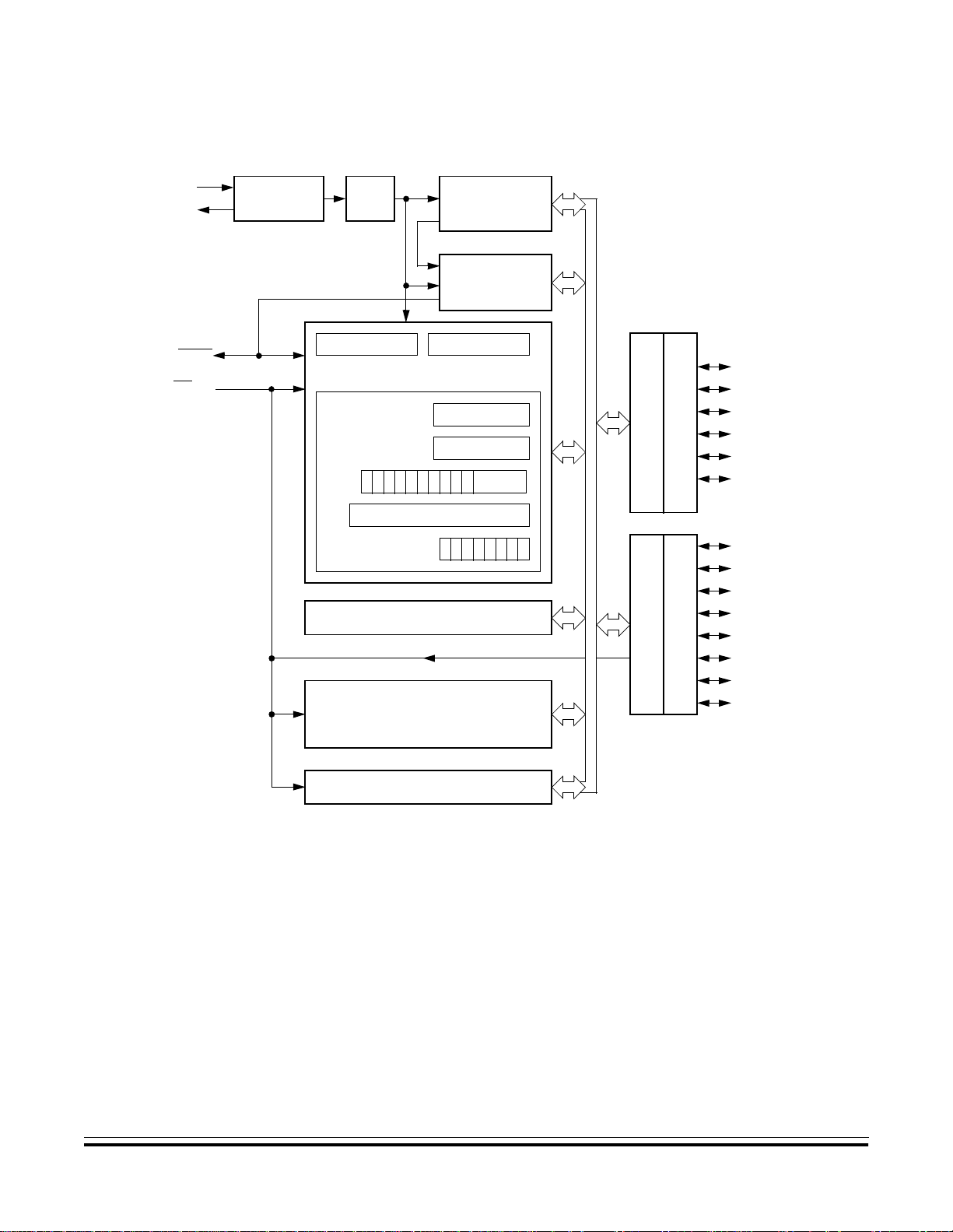
General Description
Introduction
OSC1
OSC2
RESET
IRQ/V
PP
INTERNAL
OSCILLATOR
DIVIDE
BY ³2
68HC05 CPU
CPU REGISTERS
0000000011
PROGRAM COUNTER
CONDITION CODE
REGISTER
STATIC RAM (SRAM) — 64 BYTES
USER EPROM — 1240 BYTES
15-STAGE
MULTIFUNCTION
TIMER SYSTEM
WATCHDOG AND
ILLEGAL ADDRESS
ALUCPU CONTROL
ACCUMULATOR
INDEX REGISTER
111HINZC
DETECT
STK PTR
PB5
PB4
PB3
PB2
PB1
PB0
PA7*
PA6*
PA5*
PA4*
PORT A PORT B
DATA DIRECTION REGISTER A DATA DIRECTION REGISTER B
*10-m A si nk capability
**External interrupt capability
PA3* *
PA2* *
PA1* *
PA0* *
MASK OPTION REGISTER (EPROM)
Figure 1-1. Block Diagram
MC68HC705J1A — Rev. 4.0 Technical Data
MOTOROLA General Description 23

General Description
1.3 Features
Features of the MC68HC705J1A include:
• Periphera l modules:
– 15-stage multifunction timer
– Computer operating properly (COP) watchdog
• 14 bidirectional input/output (I/O) lines, including:
– 10-mA sink capability on four I/O pins
– Mask option register (MOR) and software programmable
pulldowns on all I/O pins
– MOR selectable interrupt on four I/O pins, a keyboard scan
feature
• MOR selectable sensitivity on external interrupt (edge- and
level-sensitive or edge-sensitive only)
• On-chip oscillator with connections for:
– Crystal
– Ceramic resonator
– Resistor-capacitor (RC) oscillator
– External clock
• 1240 bytes of EPROM/OTPROM, including eight bytes for user
vectors
• 64 bytes of user random-access memory (RAM)
• Memory-mapped I/O registers
• Fully static operation with no minimum clock speed
• Power-saving stop, halt, wait, and data-retention modes
• External interrupt mask bit and acknowledge bit
• Illegal address reset
• Internal steer ing d iode and pullup resistor from RES ET
pin to V
DD
Technical Data MC68HC705J1A — Rev. 4.0
24 General Descri ptio n MOTOR OLA
1.4 Programmable Options
The options in Table 1-1 are programm abl e in the mask option register
(MOR).
COP watchdog timer Enabled or disabled
External interrupt triggering Edge-sensitive only or edge- and level-sensitive
General Description
Programmable Options
Table 1-1. Programmable Options
Feature Option
Port A IRQ
Port pulldown resistors Enabled or disabled
STOP instruction mode Stop mode or halt mode
Crystal oscillator internal resistor Enabled or disabled
EPROM security Enabled or disabled
Short oscillator delay counter Enabled or disabled
1.5 Pin Assignments
Figure 1-2 shows the MC68HC705J1A pin assignments.
1.5.1 VDD and V
SS
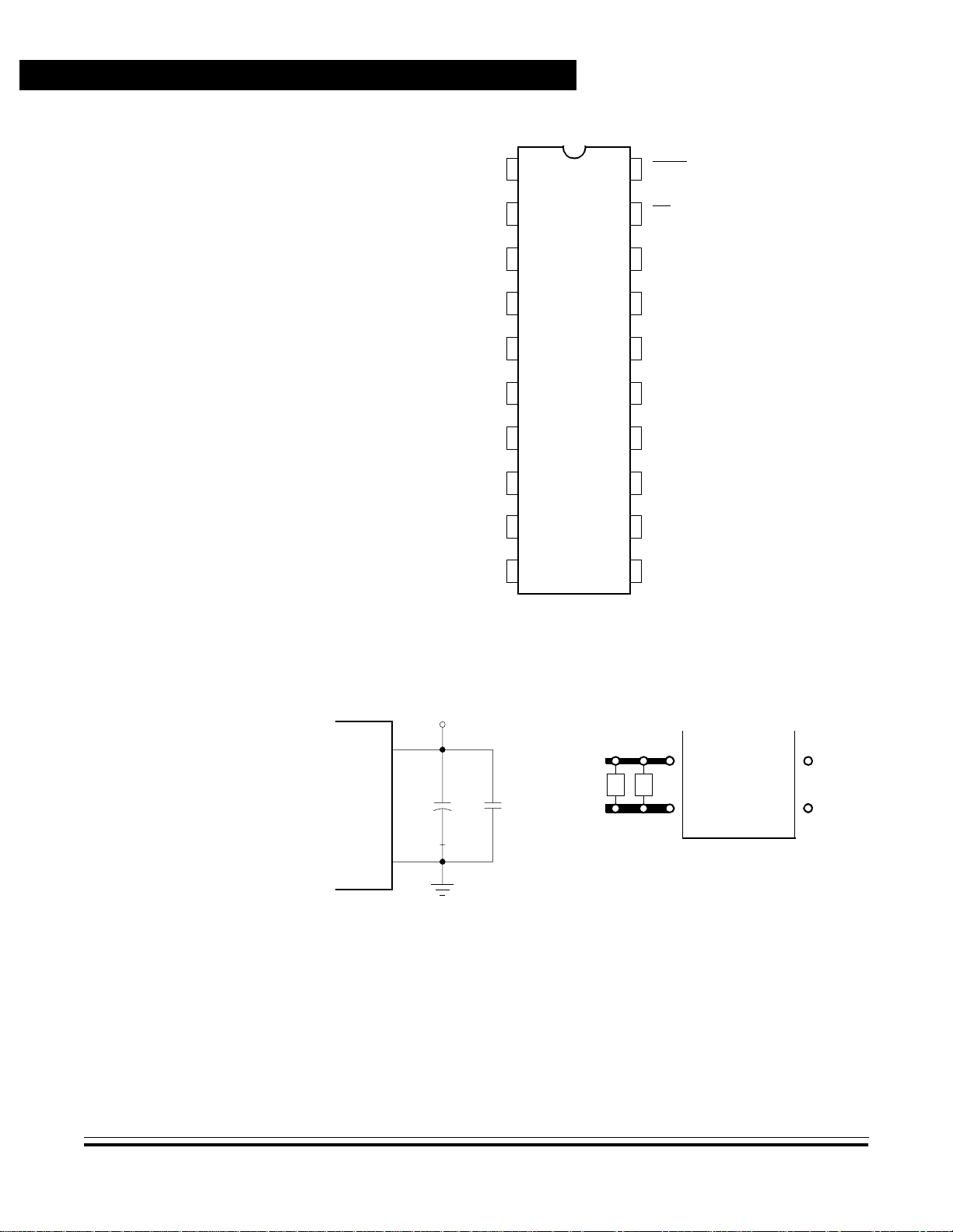
VDD and VSS are the power supply and g round pins. The MCU opera tes
from a single power supply.
Very fast signal transitions occur on the MCU pins, placing high,
short-duration current demands on the power supply. To prevent noise
problems, take special care as Figure 1-3 shows, by placing the bypas s
capacitors as close as possible to the MCU. C2 is an optional bulk
current bypass capaci tor for use in appl ications that requi re the port pi ns
to source high current levels.
pin interrupts Enabled or disabled
MC68HC705J1A — Rev. 4.0 Technical Data
MOTOROLA General Description 25
General Description
OSC1
OSC2 2
PB5 3
PB4 4
PB3 5
PB2 6
PB1 7
PB0 8
V
DD
V
SS
1
9
10
RESET
20
IRQ/V
19
12
11
PP
PA018
PA117
PA216
PA315
PA414
PA513
PA6
PA7
Figure 1-2. Pin Assignments
V+
V
MCU
DD
C1
0.1 µF
V
SS
C2
+
C2
C1
V
DD
V
SS
Figure 1-3. Bypassing Layout Recommendation
Technical Data MC68HC705J1A — Rev. 4.0
26 General Descri ptio n MOTOR OLA

1.5.2 OSC1 and OSC2
General Description
Pin Assignments
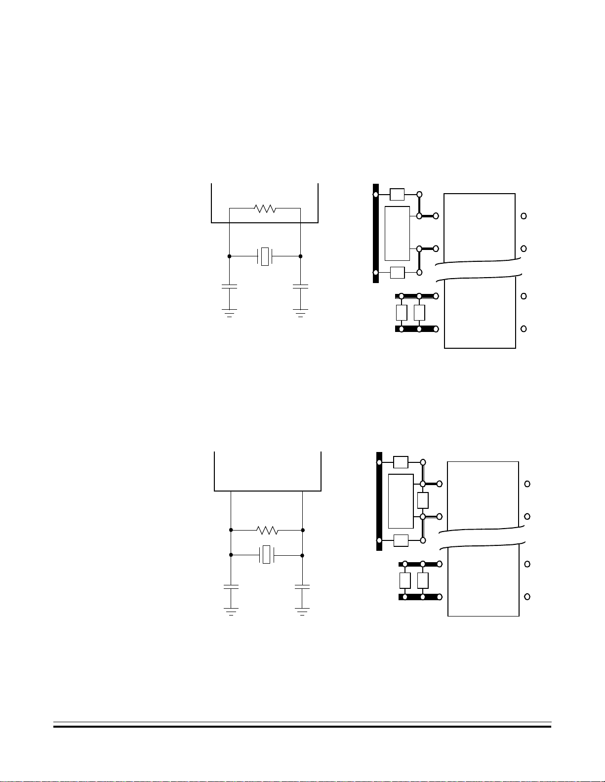
The OSC1 and OSC2 pins are the connections for the on-chip oscillator.
The oscillator can be driven by any of these:
1. Crystal (See Figure 1-4 and Figure 1-5.)
2. Ceramic resonator (See Figure 1-6 and Figure 1-7.)
3. Resistor/capacitor (RC) oscillator (Refer to Appendix A.
MC68HRC705J1A and Appendix C. MC68HSR705J1A.)
4. External clock signal (See Figure 1-8.)
1.5.2.1 Crystal Oscillator
NOTE: Use an AT-cut crystal and not an AT -strip crystal becau se the MCU can
The frequency, f
by two to produce the internal operating frequency, f
, of the oscillator or external clock source is divided
osc
.
op
Figure 1-4 and Figur e 1- 5 show a typica l crystal oscillator circuit for an
AT-cut, parallel re sonant crystal. Follow the crystal supplier’s
recommendations, as the crystal parameters determine the external
component values required to provide reliable startup and maximum
stability. The loa d capacitance values used in the oscilla tor circuit design
should include all stray layout capacitances.
To minimize out put distortion, mount the crystal an d capacitors a s close
as possible to the pins. An internal startup resistor of approximately
2MΩ is provided between OSC1 and OSC2 for the crystal oscillator as
a programmable mask option.
overdrive an AT-strip crystal.
MC68HC705J1A — Rev. 4.0 Technical Data
MOTOROLA General Description 27

General Description
V
SS
MCU
OSC1
OSC2
C3
OSC1
XTAL
OSC2
C3
27 pF
C3
27 pF
XTAL
C4
27 pF
C4
C1C2
Figure 1-4. Crystal Connections with
Oscillator Internal Resistor Mask Option
V
SS
MCU
R
OSC1
10 M¾Ω
XTAL
OSC2
27 pF
C4
C3
XTAL
C4
R
C1C2
V
DD
V
SS
OSC1
OSC2
V
DD
V
SS
Figure 1-5. Crystal Connections without
Oscillator Internal Resistor Mask Option
1.5.2.2 Ceramic Resonator Oscillator
To reduce cost, use a ceramic resonator instead of the crystal. The
circuits shown in Figure 1-6 and Figure 1-7 show ceramic resonator
circuits. Follow the resonator manufacturer’s recommendations, as the
resonator parameters determine the external component values
required for maximum stability and reliable starting. The load
capacitance values used in the o scillator circuit d esign should include all
stray capacitances.
Technical Data MC68HC705J1A — Rev. 4.0
28 General Descri ptio n MOTOR OLA
General Description
Pin Assignments
Mount the resonator and components as close as possible to the pins for
startup stabilization and to min imize output distortion. An internal startup
resistor of approximat ely 2 MΩ is provided between OSC1 and OSC2 as
a programmable mask option.
V
SS
MCU
C3
OSC1
C3
27 pF
OSC1
CERAMIC
RESON ATOR
OSC2
C4
27 pF
C4
CERAMIC
RESON ATOR
C1C2
OSC2
V
DD
V
SS
Figure 1-6. Ceramic Resonator Connections
with Oscillator Internal Resistor Mask Option
V
SS
C3
OSC1
R
CERAMIC
RESON ATOR
OSC2
OSC1
MCU
R
10 M¾Ω
OSC2
C4
V
DD
V
SS
C3
27 pF
CERAMIC
RESON ATOR
C4
27 pF
C1C2
Figure 1-7. Ceramic Resonator Connections
without Oscillator Internal Resistor Mask Option
MC68HC705J1A — Rev. 4.0 Technical Data
MOTOROLA General Description 29

General Description
1.5.2.3 RC Oscillator
1.5.2.4 External Clock
Refer to Appendix A. MC68HRC705J1A and Appendix C.
MC68HSR705J1A.
An external clock from another complementary metal-oxide
semiconductor (CMOS)-compatible device can be connected to the
OSC1 input, with the OSC2 input not connected, as shown in
Figure 1-8. This configuration is possible regardless of whether the
crystal/ceramic resonator or the RC oscillator is enabled.
MCU
1.6 RESET
OSC1
EXTERNAL
CMOS CLOCK
OSC2
Figure 1-8. External Clock Connections
Applying a logic 0 to the RE SET pin for ces the M CU to a known startup
state. An internal r eset also pulls the RESET pin low. An internal resist or
to VDD pulls the RESET pin hi gh. A steeri n g diode b etween the RESET
and V
pins discharges any RESET pin voltage when power is
DD
removed from the MCU. The RESET pin contains an internal Schmitt
trigger to improve its noise immunity as an input. Refer to Section 4.
Resets and Interrupts for more information.
Technical Data MC68HC705J1A — Rev. 4.0
30 General Descri ptio n MOTOR OLA
 Loading...