

Page 1

HC05RC16GRS/D
REV. 3.0
MC68HC05RC8
MC68HC05RC16
General Release Specification
October 24, 1996
CSIC MCU Design Center
Austin, Texas
NON-DISCLOSURE AGREEMENT REQUIRED
Page 2

General Release Specification
Motorola reserves the right to make changes without further notice to
any products herein to improve reliability, function or design. Motorola
does not assume any liability arising out of the application or use of any
product or circuit described herein; neither does it convey any license
under its patent rights nor the rights of others. Motorola products are not
designed, intended, or authorized for use as components in systems
intended for surgical implant into the body, or other applications intended
to support or sustain life, or for any other application in which the failure
of the Motorola product could create a situation where personal injury or
death may occur. Should Buyer purchase or use Motorola products for
any such unintended or unauthorized application, Buyer shall indemnify
and hold Motorola and its officers, employees, subsidiaries, affiliates,
and distributors harmless against all claims, costs, damages, and
expenses, and reasonable attorney fees arising out of, directly or
indirectly, any claim of personal injury or death associated with such
unintended or unauthorized use, even if such claim alleges that Motorola
was negligent regarding the design or manufacture of the part.
NON-DISCLOSURE AGREEMENT REQUIRED
© Motorola, Inc., 1996 MC68HC05RC16 — Rev. 3.0
2 MOTOROLA
Page 3

General Release Specification — MC68HC05RC16
Section 1. General Description . . . . . . . . . . . . . . . . . . . 15
Section 2. Memory . . . . . . . . . . . . . . . . . . . . . . . . . . . . . 27
Section 3. Central Processor Unit . . . . . . . . . . . . . . . . . 33
Section 4. Interrupts . . . . . . . . . . . . . . . . . . . . . . . . . . . . 37
Section 5. Resets . . . . . . . . . . . . . . . . . . . . . . . . . . . . . . . 45
List of Sections
Section 6. Low-Power Modes . . . . . . . . . . . . . . . . . . . . 53
Section 7. Parallel Input/Output (I/O) . . . . . . . . . . . . . . 57
Section 8. Core Timer . . . . . . . . . . . . . . . . . . . . . . . . . . . 61
Section 9. Carrier Modulator Transmitter (CMT) . . . . . . 67
Section 10. Instruction Set . . . . . . . . . . . . . . . . . . . . . . . 85
Section 11. Electrical Specifications . . . . . . . . . . . . . . 103
Section 12. Mechanical Specifications . . . . . . . . . . . 111
Section 13. Ordering Information . . . . . . . . . . . . . . . . 115
Appendix A. MC68HC05RC8 . . . . . . . . . . . . . . . . . . . . 119
MC68HC05RC16 — Rev. 3.0 General Release Specification
MOTOROLA List of Sections 3
Page 4

List of Sections
General Release Specification MC68HC05RC16 — Rev. 3.0
4 List of Sections MOTOROLA
Page 5

General Release Specification — MC68HC05RC16
Section 1. General Description
1.1 Contents . . . . . . . . . . . . . . . . . . . . . . . . . . . . . . . . . . . . . . . . . .15
1.2 Introduction. . . . . . . . . . . . . . . . . . . . . . . . . . . . . . . . . . . . . . . .16
1.3 Features . . . . . . . . . . . . . . . . . . . . . . . . . . . . . . . . . . . . . . . . . .16
1.4 Mask Options . . . . . . . . . . . . . . . . . . . . . . . . . . . . . . . . . . . . . .19
1.5 Signal Description. . . . . . . . . . . . . . . . . . . . . . . . . . . . . . . . . . .21
1.5.1 V
1.5.2
1.5.3 OSC1 and OSC2. . . . . . . . . . . . . . . . . . . . . . . . . . . . . . . . .24
1.5.4
1.5.5
1.5.6 IRO . . . . . . . . . . . . . . . . . . . . . . . . . . . . . . . . . . . . . . . . . . .25
1.5.7 PA0–PA7. . . . . . . . . . . . . . . . . . . . . . . . . . . . . . . . . . . . . . .25
1.5.8 PB0–PB7. . . . . . . . . . . . . . . . . . . . . . . . . . . . . . . . . . . . . . .25
1.5.9 PC0–PC3 (PC4–PC7). . . . . . . . . . . . . . . . . . . . . . . . . . . . .26
and VSS . . . . . . . . . . . . . . . . . . . . . . . . . . . . . . . . . . . .23
DD
IRQ (Maskable Interrupt Request) . . . . . . . . . . . . . . . . . . .23
RESET . . . . . . . . . . . . . . . . . . . . . . . . . . . . . . . . . . . . . . . .25
LPRST. . . . . . . . . . . . . . . . . . . . . . . . . . . . . . . . . . . . . . . . .25
Table of Contents
Section 2. Memory
2.1 Contents . . . . . . . . . . . . . . . . . . . . . . . . . . . . . . . . . . . . . . . . . .27
2.2 Introduction. . . . . . . . . . . . . . . . . . . . . . . . . . . . . . . . . . . . . . . .27
2.3 Memory Map. . . . . . . . . . . . . . . . . . . . . . . . . . . . . . . . . . . . . . .27
2.3.1 ROM . . . . . . . . . . . . . . . . . . . . . . . . . . . . . . . . . . . . . . . . . .30
2.3.2 ROM Security . . . . . . . . . . . . . . . . . . . . . . . . . . . . . . . . . . .30
2.3.3 RAM . . . . . . . . . . . . . . . . . . . . . . . . . . . . . . . . . . . . . . . . . .31
2.4 Input/Output Programming . . . . . . . . . . . . . . . . . . . . . . . . . . . .31
MC68HC05RC16 — Rev. 3.0 General Release Specification
MOTOROLA Table of Contents 5
Page 6

Table of Contents
Section 3. Central Processor Unit
3.1 Contents . . . . . . . . . . . . . . . . . . . . . . . . . . . . . . . . . . . . . . . . . .33
3.2 Introduction. . . . . . . . . . . . . . . . . . . . . . . . . . . . . . . . . . . . . . . .33
3.3 Accumulator . . . . . . . . . . . . . . . . . . . . . . . . . . . . . . . . . . . . . . .34
3.4 Index Register. . . . . . . . . . . . . . . . . . . . . . . . . . . . . . . . . . . . . .34
3.5 Condition Code Register. . . . . . . . . . . . . . . . . . . . . . . . . . . . . .35
3.6 Stack Pointer . . . . . . . . . . . . . . . . . . . . . . . . . . . . . . . . . . . . . .36
3.7 Program Counter . . . . . . . . . . . . . . . . . . . . . . . . . . . . . . . . . . .36
Section 4. Interrupts
4.1 Contents . . . . . . . . . . . . . . . . . . . . . . . . . . . . . . . . . . . . . . . . . .37
4.2 Introduction. . . . . . . . . . . . . . . . . . . . . . . . . . . . . . . . . . . . . . . .37
4.3 CPU Interrupt Processing. . . . . . . . . . . . . . . . . . . . . . . . . . . . .38
4.4 Reset Interrupt Sequence. . . . . . . . . . . . . . . . . . . . . . . . . . . . .39
4.5 Software Interrupt (SWI). . . . . . . . . . . . . . . . . . . . . . . . . . . . . .39
4.6 Hardware Interrupts . . . . . . . . . . . . . . . . . . . . . . . . . . . . . . . . .41
4.7 External Interrupt (
4.8 External Interrupt Timing . . . . . . . . . . . . . . . . . . . . . . . . . . . . .42
4.9 Carrier Modulator Transmitter Interrupt (CMT). . . . . . . . . . . . .42
4.10 Core Timer Interrupt . . . . . . . . . . . . . . . . . . . . . . . . . . . . . . . . .43
IRQ/Port B Keyscan). . . . . . . . . . . . . . . . . .41
Section 5. Resets
5.1 Contents . . . . . . . . . . . . . . . . . . . . . . . . . . . . . . . . . . . . . . . . . .45
5.2 Introduction. . . . . . . . . . . . . . . . . . . . . . . . . . . . . . . . . . . . . . . .45
5.3 External Reset (
5.4 Low-Power External Reset (LPRST) . . . . . . . . . . . . . . . . . . . .48
RESET). . . . . . . . . . . . . . . . . . . . . . . . . . . . . .46
General Release Specification MC68HC05RC16 — Rev. 3.0
6 Table of Contents MOTOROLA
Page 7

Table of Contents
5.5 Internal Resets . . . . . . . . . . . . . . . . . . . . . . . . . . . . . . . . . . . . .48
5.5.1 Power-On Reset (POR). . . . . . . . . . . . . . . . . . . . . . . . . . . .48
5.5.2 Computer Operating Properly Reset (COPR). . . . . . . . . . .49
5.5.2.1 Resetting the COP. . . . . . . . . . . . . . . . . . . . . . . . . . . . . .49
5.5.2.2 COP During Wait Mode . . . . . . . . . . . . . . . . . . . . . . . . . .49
5.5.2.3 COP During Stop Mode . . . . . . . . . . . . . . . . . . . . . . . . . .49
5.5.2.4 COP Watchdog Timer Considerations. . . . . . . . . . . . . . .50
5.5.2.5 COP Register. . . . . . . . . . . . . . . . . . . . . . . . . . . . . . . . . .51
5.5.3 Illegal Address. . . . . . . . . . . . . . . . . . . . . . . . . . . . . . . . . . .51
Section 6. Low-Power Modes
6.1 Contents . . . . . . . . . . . . . . . . . . . . . . . . . . . . . . . . . . . . . . . . . .53
6.2 Introduction. . . . . . . . . . . . . . . . . . . . . . . . . . . . . . . . . . . . . . . .53
6.3 Stop Mode . . . . . . . . . . . . . . . . . . . . . . . . . . . . . . . . . . . . . . . .53
6.4 Stop Recovery . . . . . . . . . . . . . . . . . . . . . . . . . . . . . . . . . . . . .54
6.5 Wait Mode. . . . . . . . . . . . . . . . . . . . . . . . . . . . . . . . . . . . . . . . .54
6.6 Low-Power Reset . . . . . . . . . . . . . . . . . . . . . . . . . . . . . . . . . . .55
Section 7. Parallel Input/Output (I/O)
7.1 Contents . . . . . . . . . . . . . . . . . . . . . . . . . . . . . . . . . . . . . . . . . .57
7.2 Introduction. . . . . . . . . . . . . . . . . . . . . . . . . . . . . . . . . . . . . . . .57
7.3 Port A . . . . . . . . . . . . . . . . . . . . . . . . . . . . . . . . . . . . . . . . . . . .57
7.4 Port B . . . . . . . . . . . . . . . . . . . . . . . . . . . . . . . . . . . . . . . . . . . .58
7.5 Port C . . . . . . . . . . . . . . . . . . . . . . . . . . . . . . . . . . . . . . . . . . . .58
7.6 Input/Output Programming . . . . . . . . . . . . . . . . . . . . . . . . . . . .59
MC68HC05RC16 — Rev. 3.0 General Release Specification
MOTOROLA Table of Contents 7
Page 8

Table of Contents
Section 8. Core Timer
8.1 Contents . . . . . . . . . . . . . . . . . . . . . . . . . . . . . . . . . . . . . . . . . .61
8.2 Introduction. . . . . . . . . . . . . . . . . . . . . . . . . . . . . . . . . . . . . . . .61
8.3 Core Timer Control and Status Register. . . . . . . . . . . . . . . . . .63
8.4 Core Timer Counter Register . . . . . . . . . . . . . . . . . . . . . . . . . .65
8.5 Computer Operating Properly (COP) Reset. . . . . . . . . . . . . . .66
8.6 Timer During Wait Mode. . . . . . . . . . . . . . . . . . . . . . . . . . . . . .66
Section 9. Carrier Modulator Transmitter (CMT)
9.1 Contents . . . . . . . . . . . . . . . . . . . . . . . . . . . . . . . . . . . . . . . . . .67
9.2 Introduction. . . . . . . . . . . . . . . . . . . . . . . . . . . . . . . . . . . . . . . .67
9.3 Overview. . . . . . . . . . . . . . . . . . . . . . . . . . . . . . . . . . . . . . . . . .68
9.4 Carrier Generator . . . . . . . . . . . . . . . . . . . . . . . . . . . . . . . . . . .70
9.4.1 Time Counter. . . . . . . . . . . . . . . . . . . . . . . . . . . . . . . . . . . .71
9.4.2 Carrier Generator Data Registers
(CHR1, CLR1, CHR2, and CLR2) . . . . . . . . . . . . . . . . .72
9.5 Modulator . . . . . . . . . . . . . . . . . . . . . . . . . . . . . . . . . . . . . . . . .74
9.5.1 Time Mode . . . . . . . . . . . . . . . . . . . . . . . . . . . . . . . . . . . . .76
9.5.2 FSK Mode . . . . . . . . . . . . . . . . . . . . . . . . . . . . . . . . . . . . . .77
9.5.3 Extended Space Operation. . . . . . . . . . . . . . . . . . . . . . . . .78
9.5.3.1 End Of Cycle (EOC) Interrupt . . . . . . . . . . . . . . . . . . . . .79
9.5.3.2 Modulator Control and Status Register . . . . . . . . . . . . . .80
9.5.4 Modulator Period Data Registers
(MDR1, MDR2, and MDR3) . . . . . . . . . . . . . . . . . . . . . .83
General Release Specification MC68HC05RC16 — Rev. 3.0
8 Table of Contents MOTOROLA
Page 9

Table of Contents
Section 10. Instruction Set
10.1 Contents . . . . . . . . . . . . . . . . . . . . . . . . . . . . . . . . . . . . . . . . . .85
10.2 Introduction. . . . . . . . . . . . . . . . . . . . . . . . . . . . . . . . . . . . . . . .86
10.3 Addressing Modes . . . . . . . . . . . . . . . . . . . . . . . . . . . . . . . . . .86
10.3.1 Inherent. . . . . . . . . . . . . . . . . . . . . . . . . . . . . . . . . . . . . . . .87
10.3.2 Immediate . . . . . . . . . . . . . . . . . . . . . . . . . . . . . . . . . . . . . .87
10.3.3 Direct. . . . . . . . . . . . . . . . . . . . . . . . . . . . . . . . . . . . . . . . . .87
10.3.4 Extended. . . . . . . . . . . . . . . . . . . . . . . . . . . . . . . . . . . . . . .87
10.3.5 Indexed, No Offset . . . . . . . . . . . . . . . . . . . . . . . . . . . . . . .88
10.3.6 Indexed, 8-Bit Offset . . . . . . . . . . . . . . . . . . . . . . . . . . . . . .88
10.3.7 Indexed,16-Bit Offset. . . . . . . . . . . . . . . . . . . . . . . . . . . . . .88
10.3.8 Relative . . . . . . . . . . . . . . . . . . . . . . . . . . . . . . . . . . . . . . . .89
10.4 Instruction Types . . . . . . . . . . . . . . . . . . . . . . . . . . . . . . . . . . .89
10.4.1 Register/Memory Instructions . . . . . . . . . . . . . . . . . . . . . . .90
10.4.2 Read-Modify-Write Instructions. . . . . . . . . . . . . . . . . . . . . .91
10.4.3 Jump/Branch Instructions . . . . . . . . . . . . . . . . . . . . . . . . . .92
10.4.4 Bit Manipulation Instructions . . . . . . . . . . . . . . . . . . . . . . . .94
10.4.5 Control Instructions . . . . . . . . . . . . . . . . . . . . . . . . . . . . . . .95
10.5 Instruction Set Summary . . . . . . . . . . . . . . . . . . . . . . . . . . . . .96
Section 11. Electrical Specifications
11.1 Contents . . . . . . . . . . . . . . . . . . . . . . . . . . . . . . . . . . . . . . . . .103
11.2 Introduction. . . . . . . . . . . . . . . . . . . . . . . . . . . . . . . . . . . . . . .103
11.3 Maximum Ratings. . . . . . . . . . . . . . . . . . . . . . . . . . . . . . . . . .104
11.4 Operating Range . . . . . . . . . . . . . . . . . . . . . . . . . . . . . . . . . .105
11.5 Thermal Characteristics . . . . . . . . . . . . . . . . . . . . . . . . . . . . .105
11.6 DC Electrical Characteristics (5.0 Vdc). . . . . . . . . . . . . . . . . .106
11.7 DC Electrical Characteristics (2.2 Vdc). . . . . . . . . . . . . . . . . .107
11.8 Control Timing (5.0 Vdc and 2.2 V
) . . . . . . . . . . . . . . . . . . .109
dc
MC68HC05RC16 — Rev. 3.0 General Release Specification
MOTOROLA Table of Contents 9
Page 10

Table of Contents
Section 12. Mechanical Specifications
12.1 Contents . . . . . . . . . . . . . . . . . . . . . . . . . . . . . . . . . . . . . . . . .111
12.2 Introduction. . . . . . . . . . . . . . . . . . . . . . . . . . . . . . . . . . . . . . .111
12.3 28-Pin Plastic Dual In-Line Package
(Case 710-02) . . . . . . . . . . . . . . . . . . . . . . . . . . . . . . . . . .112
12.4 28-Pin Small Outline Integrated Circuit Package
(Case 751F-04) . . . . . . . . . . . . . . . . . . . . . . . . . . . . . . . . .112
12.5 44-Pin Plastic Leaded Chip Carrier Package
(Case 777-02) . . . . . . . . . . . . . . . . . . . . . . . . . . . . . . . . . .113
Section 13. Ordering Information
13.1 Contents . . . . . . . . . . . . . . . . . . . . . . . . . . . . . . . . . . . . . . . . .115
13.2 Introduction. . . . . . . . . . . . . . . . . . . . . . . . . . . . . . . . . . . . . . .115
13.3 MCU Ordering Forms . . . . . . . . . . . . . . . . . . . . . . . . . . . . . . .115
13.4 Application Program Media. . . . . . . . . . . . . . . . . . . . . . . . . . .116
13.5 ROM Program Verification . . . . . . . . . . . . . . . . . . . . . . . . . . .117
13.6 ROM Verification Units (RVUs). . . . . . . . . . . . . . . . . . . . . . . .118
13.7 MC Order Numbers . . . . . . . . . . . . . . . . . . . . . . . . . . . . . . . .118
Appendix A. MC68HC05RC8
A.1 Contents . . . . . . . . . . . . . . . . . . . . . . . . . . . . . . . . . . . . . . . . .119
A.2 Introduction . . . . . . . . . . . . . . . . . . . . . . . . . . . . . . . . . . . . . .119
A.3 Memory Map . . . . . . . . . . . . . . . . . . . . . . . . . . . . . . . . . . . . .119
General Release Specification MC68HC05RC16 — Rev. 3.0
10 Table of Contents MOTOROLA
Page 11

General Release Specification — MC68HC05RC16
Figure Title Page
1-1 MC68HC05RC16 Block Diagram. . . . . . . . . . . . . . . . . . . . .18
1-2 28-Pin DIP Pinout. . . . . . . . . . . . . . . . . . . . . . . . . . . . . . . . .21
1-3 28-Pin SOIC Pinout . . . . . . . . . . . . . . . . . . . . . . . . . . . . . . .22
1-4 44-Pin PLCC Pinout. . . . . . . . . . . . . . . . . . . . . . . . . . . . . . .22
1-5 Oscillator Connections . . . . . . . . . . . . . . . . . . . . . . . . . . . . .24
2-1 MC68HC05RC16 Memory Map . . . . . . . . . . . . . . . . . . . . . .28
2-2 I/O Registers . . . . . . . . . . . . . . . . . . . . . . . . . . . . . . . . . . . .29
3-1 Programming Model. . . . . . . . . . . . . . . . . . . . . . . . . . . . . . .33
3-2 Stacking Order . . . . . . . . . . . . . . . . . . . . . . . . . . . . . . . . . . .34
List of Figures
4-1 Interrupt Processing Flowchart. . . . . . . . . . . . . . . . . . . . . . .40
4-2 IRQ Function Block Diagram . . . . . . . . . . . . . . . . . . . . . . . .41
5-1 Reset Block Diagram . . . . . . . . . . . . . . . . . . . . . . . . . . . . . .46
5-2 Reset and POR Timing Diagram . . . . . . . . . . . . . . . . . . . . .47
5-3 COP Watchdog Timer Location . . . . . . . . . . . . . . . . . . . . . .51
6-1 Stop Recovery Timing Diagram . . . . . . . . . . . . . . . . . . . . . .54
6-2 Stop/Wait Flowchart. . . . . . . . . . . . . . . . . . . . . . . . . . . . . . .56
7-1 Port B Pullup Option. . . . . . . . . . . . . . . . . . . . . . . . . . . . . . .58
7-2 I/O Circuitry . . . . . . . . . . . . . . . . . . . . . . . . . . . . . . . . . . . . .60
8-1 Core Timer Block Diagram. . . . . . . . . . . . . . . . . . . . . . . . . .62
8-2 Core Timer Control and Status Register (CTCSR) . . . . . . .63
8-3 Core Timer Counter Register (CTCR) . . . . . . . . . . . . . . . . .65
MC68HC05RC16 — Rev. 3.0 General Release Specification
MOTOROLA List of Figures 11
Page 12

List of Figures
Figure Title Page
9-1 Carrier Modulator Transmitter Module Block Diagram. . . . .69
9-2 Carrier Generator Block Diagram. . . . . . . . . . . . . . . . . . . . .70
9-3 Carrier Generator Data Register CHR1 . . . . . . . . . . . . . . . .72
9-4 Carrier Generator Data Register CLR1 . . . . . . . . . . . . . . . .72
9-5 Carrier Generator Data Register CHR2 . . . . . . . . . . . . . . . .72
9-6 Carrier Generator Data Register CLR2 . . . . . . . . . . . . . . . .73
9-7 Modulator Block Diagram. . . . . . . . . . . . . . . . . . . . . . . . . . .75
9-8 CMT Operation in Time Mode . . . . . . . . . . . . . . . . . . . . . . .77
9-9 Extended Space Operation . . . . . . . . . . . . . . . . . . . . . . . . .79
9-10 Modulator Control and Status Register (MCSR) . . . . . . . . .80
9-11 Modulator Period Data Register MDR1 . . . . . . . . . . . . . . . .83
9-12 Modulator Period Data Register MDR2 . . . . . . . . . . . . . . . .83
9-13 Modulator Period Data Register MDR3 . . . . . . . . . . . . . . . .83
11-1 Maximum Supply Current versus Internal
Clock Frequency . . . . . . . . . . . . . . . . . . . . . . . . . . . . . .108
A-1 MC68HC05RC8 Memory Map . . . . . . . . . . . . . . . . . . . . .120
General Release Specification MC68HC05RC16 — Rev. 3.0
12 List of Figures MOTOROLA
Page 13

General Release Specification — MC68HC05RC16
Table Title Page
4-1 Vector Address for Interrupts and Reset................................38
5-1 COP Watchdog Timer Recommendations .............................50
7-1 I/O Pin Functions....................................................................59
8-1 RTI and COP Rates at 4.096 MHz Oscillator.........................64
10-1 Register/Memory Instructions.................................................90
10-2 Read-Modify-Write Instructions..............................................91
10-3 Jump and Branch Instructions................................................93
10-4 Bit Manipulation Instructions...................................................94
10-5 Control Instructions.................................................................95
10-6 Instruction Set Summary........................................................96
10-7 Opcode Map.........................................................................102
List of Tables
13-1 MC Order Numbers..............................................................118
MC68HC05RC16 — Rev. 3.0 General Release Specification
MOTOROLA List of Tables 13
Page 14

List of Tables
General Release Specification MC68HC05RC16 — Rev. 3.0
14 List of Tables MOTOROLA
Page 15

General Release Specification — MC68HC05RC16
Section 1. General Description
1.1 Contents
1.2 Introduction. . . . . . . . . . . . . . . . . . . . . . . . . . . . . . . . . . . . . . . .16
1.3 Features . . . . . . . . . . . . . . . . . . . . . . . . . . . . . . . . . . . . . . . . . .16
1.4 Mask Options . . . . . . . . . . . . . . . . . . . . . . . . . . . . . . . . . . . . . .19
1.5 Signal Description. . . . . . . . . . . . . . . . . . . . . . . . . . . . . . . . . . .21
1.5.1 V
1.5.2
1.5.3 OSC1 and OSC2. . . . . . . . . . . . . . . . . . . . . . . . . . . . . . . . .24
1.5.4
1.5.5
1.5.6 IRO . . . . . . . . . . . . . . . . . . . . . . . . . . . . . . . . . . . . . . . . . . .25
1.5.7 PA0–PA7. . . . . . . . . . . . . . . . . . . . . . . . . . . . . . . . . . . . . . .25
1.5.8 PB0–PB7. . . . . . . . . . . . . . . . . . . . . . . . . . . . . . . . . . . . . . .25
1.5.9 PC0–PC3 (PC4–PC7). . . . . . . . . . . . . . . . . . . . . . . . . . . . .26
and VSS . . . . . . . . . . . . . . . . . . . . . . . . . . . . . . . . . . . .23
DD
IRQ (Maskable Interrupt Request) . . . . . . . . . . . . . . . . . . .23
RESET . . . . . . . . . . . . . . . . . . . . . . . . . . . . . . . . . . . . . . . .25
LPRST. . . . . . . . . . . . . . . . . . . . . . . . . . . . . . . . . . . . . . . . .25
MC68HC05RC16 — Rev. 3.0 General Release Specification
MOTOROLA General Description 15
Page 16

General Description
1.2 Introduction
The MC68HC05RC16 is a low-cost addition to the M68HC05 Family of
microcontrollers (MCUs) and is suitable for remote control applications.
This device contains the HC05 central processing unit (CPU) core,
including the 14-stage core timer with real-time interrupt (RTI) and
computer operating properly (COP) watchdog systems. On-chip
peripherals include a carrier modulator transmitter. The 16-kbyte
memory map has 15,936 bytes of user ROM and 352 bytes of RAM.
There are 20 input/output (I/O) lines (eight having keyscan
pullups/interrupts) and a low-power reset pin. This device is available in
28-pin small outline integrated circuit (SOIC), 28-pin dual in-line (DIP),
and 44-pin plastic leaded chip carrier (PLCC) packages. Four additional
I/O lines are available for bond out on the higher pin count package.
1.3 Features
Features for the MC68HC05RC16 include:
• Low Cost
• HC05 Core
• 28-Pin Plastic Dual In-Line (PDIP), Small Outline Integrated
Circuit (SOIC), or Plastic Leaded Chip Carrier (PLCC) Packages
• On-Chip Oscillator with Crystal/Ceramic Resonator
• 4-MHz Maximum Oscillator Frequency at 5 V and 2.2 V Supply
• Fully Static Operation
• 15,936 Bytes of User ROM
• 64 Bytes of Burn-In ROM
• 352 Bytes of On-Chip RAM
• 14-Stage Core Timer with Real-Time Interrupt (RTI) and
Computer Operating Properly (COP) Watchdog Circuits
• Carrier Modulator Transmitter Supporting Baseband, Pulse
Length Modulator (PLM), and Frequency Shift Keying (FSK)
Protocols
General Release Specification MC68HC05RC16 — Rev. 3.0
16 General Description MOTOROLA
Page 17

General Description
Features
• Low-Power Reset Pin
• 20 Bidirectional I/O Lines (Four Additional I/O Lines Available for
Bond Out in 44-Lead PLCC Package)
• Mask Programmable Pullups and Interrupts on Eight Port Pins
(PB0–PB7)
• High-Current Infrared (IR) Drive Pin
• High-Current Port Pin (PC0)
• Power-Saving Stop and Wait Modes
• Mask Selectable Options:
– COP Watchdog Timer
– STOP Instruction Disable
– Edge-Sensitive or Edge- and Level-Sensitive Interrupt Trigger
NOTE:
– Port B Pullups for Keyscan
• Illegal Address Reset
• ROM Security Feature
A line over a signal name indicates an active low signal. For example,
RESET is active low.
MC68HC05RC16 — Rev. 3.0 General Release Specification
MOTOROLA General Description 17
Page 18
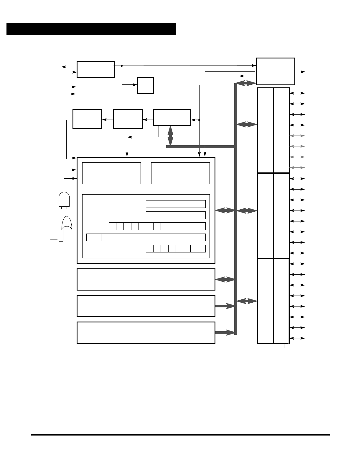
General Description
OSC2
OSC1
V
DD
V
SS
RESET
LPRST
IRQ
IRQEN
OSCILLATOR
COP
SYSTEM
CONTROL
CPU REGISTERS
0
0
CONDITION CODE REGISTER
CPU
0
SYSTEM
0
÷ 2
RTI
M68HC05 CPU
0
0
0
1
PROGRAM COUNTER
1
INTERNAL
PROCESSOR
CLOCK
CORE TIMER
SYSTEM
ALU
ACCUMULATOR
INDEX REGISTER
1
STACK POINTER
I
H
1
1
CARRIER
MODULATOR
IRQEN
Z
N
C
TRANSMITTER
PORT C
DATA DIRECTION REGISTER
PORT A
DATA DIRECTION REGISTER
IRO
PC0
PC1
PC2
PC3
PC4*
PC5*
PC6*
PC7*
PA0
PA1
PA2
PA3
PA4
PA5
PA6
PA7
PB0
SRAM — 352 BYTES
ROM — 15,936 BYTES
BURN-IN ROM — 64 BYTES
* Marked pins are available only 44-lead PLCC package.
PORT B
KEYSCAN PULLUPS
DATA DIRECTION REGISTER
PB1
PB2
PB3
PB4
PB5
PB6
PB7
Figure 1-1. MC68HC05RC16 Block Diagram
General Release Specification MC68HC05RC16 — Rev. 3.0
18 General Description MOTOROLA
Page 19

1.4 Mask Options
General Description
Mask Options
There are 11 total mask options on the MC68HC05RC16 including:
• Eight port B pullups
• IRQ sensitivity
• COP enable/disable
• STOP enable/disable
These are nonprogrammable options in that they are selected at the time
of code submission (when masks are made). These options are as
follows:
PB7PU — Port B7 Pullup/Interrupt
This bit enables or disables the pullup/interrupt on port B, bit 7.
1 = Enables the pullup/interrupt
0 = Disables the pullup/interrupt
PB6PU — Port B6 Pullup/Interrupt
This option enables or disables the pullup/interrupt on port B, bit 6.
1 = Enables pullup/interrupt
0 = Disables pullup/interrupt
PB5PU — Port B5 Pullup/Interrupt
This option enables or disables the pullup/interrupt on port B, bit 5.
1 = Enables pullup/interrupt
0 = Disables pullup/interrupt
PB4PU — Port B4 Pullup/Interrupt
This option enables or disables the pullup/interrupt on port B, bit 4.
1 = Enables pullup/interrupt
0 = Disables pullup/interrupt
PB3PU — Port B3 Pullup/Interrupt
This option enables or disables the pullup/interrupt on port B, bit 3.
1 = Enables pullup/interrupt
0 = Disables pullup/interrupt
MC68HC05RC16 — Rev. 3.0 General Release Specification
MOTOROLA General Description 19
Page 20

General Description
PB2PU — Port B2 Pullup/Interrupt
PB1PU — Port B1 Pullup/Interrupt
PB0PU — Port B0 Pullup/Interrupt
COPEN — COP Enable
This option enables or disables the pullup/interrupt on port B, bit 2.
1 = Enables pullup/interrupt
0 = Disables pullup/interrupt
This option enables or disables the pullup/interrupt on port B, bit 1.
1 = Enables pullup/interrupt
0 = Disables pullup/interrupt
This option enables or disables the pullup/interrupt on port B, bit 0.
1 = Enables pullup/interrupt
0 = Disables pullup/interrupt
NOTE:
When the COP option is selected (COPEN = 1), the COP watchdog
timer is enabled.
When the COP option is deselected (COPEN = 0), the COP watchdog
timer is disabled.
STOPEN — STOP Instruction Enable
When the STOP option is selected (STOPEN = 1), the STOP
instruction is enabled.
When the STOP option is deselected (STOPEN = 0), the STOP
instruction is equivalent to a WAIT instruction.
IRQ — IRQ sensitivity
When the IRQ option is selected (IRQ = 1), edge- and level-sensitive
IRQ is enabled.
When the IRQ option is deselected (IRQ = 0), edge-only sensitive IRQ
is enabled.
The port B keyscan interrupt sensitivity will match that of the IRQ
sensitivity. (See 4.7 External Interrupt (IRQ/Port B Keyscan) for more
information.)
General Release Specification MC68HC05RC16 — Rev. 3.0
20 General Description MOTOROLA
Page 21
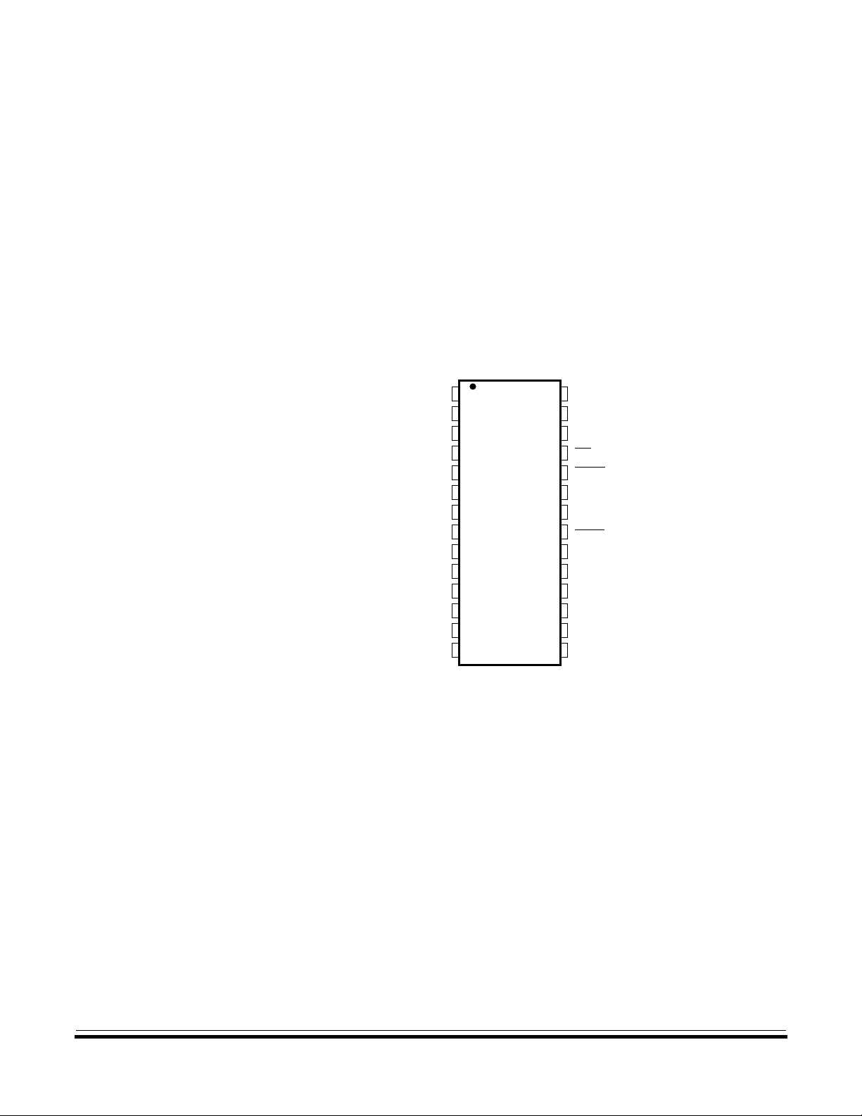
1.5 Signal Description
The MC68HC05RC16 is available in
1. 28-pin dual-in-line package (DIP) see Figure 1-2
2. 28-pin small outline integrated circuit (SOIC) package
3. 44-pin plastic leaded chip carrier (PLCC) package seeFigure 1-4
The signals are described in the following subsections.
see Figure 1-3
PB0
PB1
PB2
PB3
PB4
PB5
PB6
PB7
PA0
PA1
PA2
PA3
PA4
PA5
General Description
Signal Description
1
2
3
4
5
6
7
8
9
10
11
12
13
14
28
OSC1
27
OSC2
26
V
DD
25
IRQ
RESET
24
23
IRO
22
V
SS
21
LPRST
PC3
20
PC2
19
18
PC1
PC0
17
PA7
16
PA6
15
Figure 1-2. 28-Pin DIP Pinout
MC68HC05RC16 — Rev. 3.0 General Release Specification
MOTOROLA General Description 21
Page 22
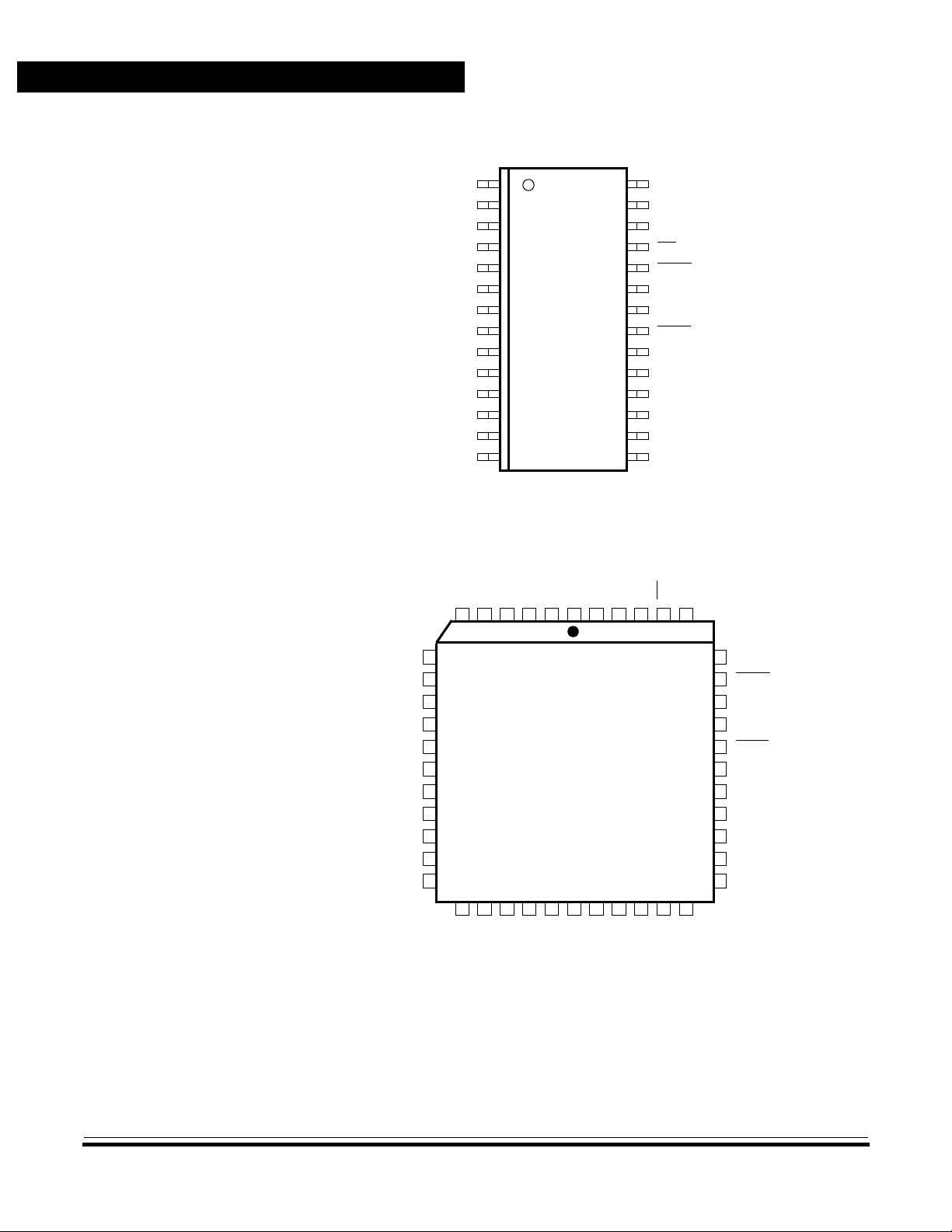
General Description
PB0 OSC1
PB1
PB2
PB3
PB4
PB5
PB6
PB7
PA0
PA1
PA2
PA3
PA4
PA5
1
2
3
4
5
6
7
8
9
10
11
12
13
14
Figure 1-3. 28-Pin SOIC Pinout
NC
PB0
2
22
OSC1
1
44
23
24
NC
PB4
PB5
PB6
PB7
NC
PC6
PC7
PA0
PA1
NC
NC
PB3
PB2
PB1
6
5
4
3
7
8
9
10
11
12
13
14
15
16
17
18
19
20
21
28
27
26
25
24
23
22
21
20
19
18
17
16
15
OSC2
43
25
OSC2
V
DD
IRQ
RESET
IRO
V
SS
LPRST
PC3
PC2
PC1
PC0
PA7
PA6
VDDIRQ
42
41
26
27
NC
40
28
NC
39
RESET
38
IRO
37
V
36
SS
LPRST
35
NC
34
PC5
33
PC4
32
PC3
31
PC2
30
NC
29
NC
PA2
PA3
PA4
NOTE: NC = No Connect
All no connects should be tied to an appropriate logic
level (either VDD or VSS).
PA5NCPA6
PA7
PC0
PC1
NC
Figure 1-4. 44-Pin PLCC Pinout
General Release Specification MC68HC05RC16 — Rev. 3.0
22 General Description MOTOROLA
Page 23

General Description
Signal Description
1.5.1 VDDand V
1.5.2
IRQ (Maskable Interrupt Request)
SS
Power is supplied to the microcontroller’s digital circuits using these two
pins. V
is the positive supply and VSS is ground.
DD
In addition to suppling the EPROM with the required programming
voltage, this pin has a mask option as specified by the user that provides
one of two different choices of interrupt triggering sensitivity. The options
are:
1. Negative edge-sensitive triggering only
2. Both negative edge-sensitive and level-sensitive triggering.
The MCU completes the current instruction before it responds to the
interrupt request. When
IRQ goes low for at least one t
(see 11.8
ILIH
Control Timing (5.0 Vdc and 2.2 Vdc)), a logic 1 is latched internally to
signify that an interrupt has been requested. When the MCU completes
its current instruction, the interrupt latch is tested. If the interrupt latch
contains a logic 1 and the interrupt mask bit (I bit) in the condition code
register is clear, the MCU then begins the interrupt sequence.
If the option is selected to include level-sensitive triggering, the
requires an external resistor to V
IRQ pin contains an internal Schmitt trigger as part of its input to
The
for wired-OR operation.
DD
IRQ input
improve noise immunity.
Refer to Section 4. Interrupts for more detail.
MC68HC05RC16 — Rev. 3.0 General Release Specification
MOTOROLA General Description 23
Page 24
General Description
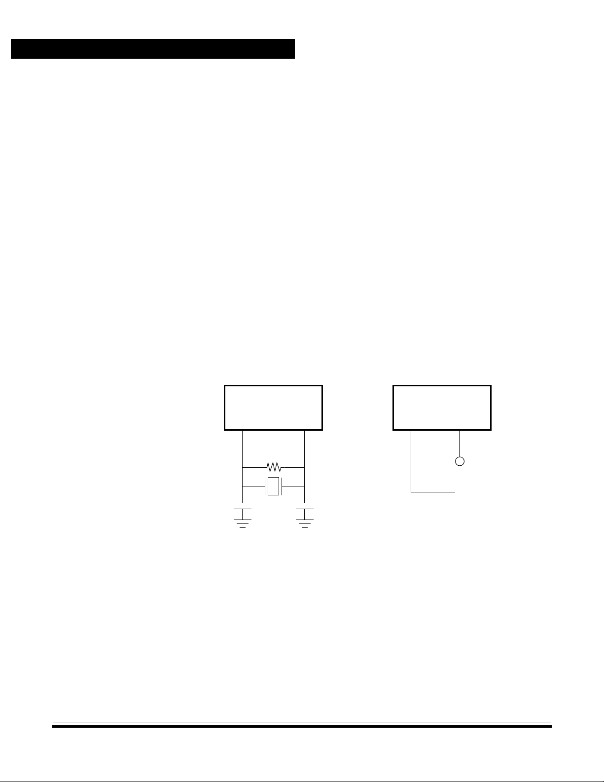
1.5.3 OSC1 and OSC2
These pins provide control input for an on-chip clock oscillator circuit. A
crystal, a ceramic resonator, or an external signal connects to these pins
to provide a system clock. The oscillator frequency is two times the
internal bus rate.
Figure 1-5 shows the recommended circuit when using a crystal. The
crystal and components should be mounted as close as possible to the
input pins to minimize output distortion and startup stabilization time.
A ceramic resonator may be used in place of the crystal in cost-sensitive
applications. Figure 1-5 (a) shows the recommended circuit for using a
ceramic resonator. The manufacturer of the particular ceramic resonator
being considered should be consulted for specific information.
An external clock should be applied to the OSC1 input with the OSC2 pin
not connected (see Figure 1-5 (b)). This setup can be used if the user
does not want to run the CPU with a crystal.
MCUMCU
OSC1 OSC2OSC1 OSC2
10 MΩ
30 pF
(a) Crystal/Ceramic Resonator (b) External Clock Source
Oscillator Connections Connections
30 pF
UNCONNECTED
<
EXTERNAL CLOCK
Figure 1-5. Oscillator Connections
General Release Specification MC68HC05RC16 — Rev. 3.0
24 General Description MOTOROLA
Page 25

1.5.4 RESET
1.5.5 LPRST
1.5.6 IRO
General Description
Signal Description
This active-low pin is used to reset the MCU to a known startup state by
pulling RESET low. The RESET pin contains an internal Schmitt trigger
as part of its input to improve noise immunity. See Section 5. Resets.
LPRST pin is an active-low pin and is used to put the MCU into
The
low-power reset mode. In low-power reset mode the MCU is held in reset
with all processor clocks halted. See Section 5. Resets.
The IRO pin is the high-current source and sink output of the carrier
modulator transmitter subsystem which is suitable for driving infrared
(IR) LED biasing logic. See Section 9. Carrier Modulator Transmitter
(CMT).
1.5.7 PA0–PA7
1.5.8 PB0–PB7
These eight I/O lines comprise port A. The state of any pin is software
programmable and all port A lines are configured as inputs during
power-on or reset. For detailed information on I/O programming, see2.4
Input/Output Programming.
These eight I/O lines comprise port B. The state of any pin is software
programmable and all port B lines are configured as inputs during
power-on or reset. Each port B I/O line has a mask optionable
pullup/interrupt for keyscan. For detailed information on I/O
programming, see 2.4 Input/Output Programming.
MC68HC05RC16 — Rev. 3.0 General Release Specification
MOTOROLA General Description 25
Page 26

General Description
1.5.9 PC0–PC3 (PC4–PC7)
These eight I/O lines comprise port C. PC0 is a high-current pin.
PC4–PC7 are available only in the 44-lead PLCC package. The state of
any pin is software programmable and all port C lines are configured as
input during power-on or reset. For detailed information on I/O
programming, see 2.4 Input/Output Programming.
NOTE:
NOTE:
Only four bits of port C are bonded out in 28-pin packages for the
MC68HC05RC16, although port C is truly an 8-bit port. Since pins
PC4–PC7 are unbonded, software should include the code to set their
respective data direction register locations to outputs to avoid floating
inputs.
Any unused inputs, I/O ports, and no connects should be tied to an
appropriate logic level (either V
or VSS). Although the I/O ports of the
DD
do not require termination, termination is recommended to reduce the
possibility of static damage.
General Release Specification MC68HC05RC16 — Rev. 3.0
26 General Description MOTOROLA
Page 27

General Release Specification — MC68HC05RC16
2.1 Contents
2.2 Introduction. . . . . . . . . . . . . . . . . . . . . . . . . . . . . . . . . . . . . . . .27
2.3 Memory Map. . . . . . . . . . . . . . . . . . . . . . . . . . . . . . . . . . . . . . .27
2.3.1 ROM . . . . . . . . . . . . . . . . . . . . . . . . . . . . . . . . . . . . . . . . . .30
2.3.2 ROM Security . . . . . . . . . . . . . . . . . . . . . . . . . . . . . . . . . . .30
2.3.3 RAM . . . . . . . . . . . . . . . . . . . . . . . . . . . . . . . . . . . . . . . . . .31
2.4 Input/Output Programming . . . . . . . . . . . . . . . . . . . . . . . . . . . .31
2.2 Introduction
Section 2. Memory
2.3 Memory Map
This section describes the organization of the on-chip memory.
The MC68HC05RC16 has a 16-Kbyte memory map consisting of user
ROM, RAM, burn-in ROM, and input/output (I/O).
Figure 2-1 shows the MC68HC05RC16 memory map in user mode.
MC68HC05RC16 — Rev. 3.0 General Release Specification
MOTOROLA Memory 27
Page 28
Memory
$0000
$001F
$0020
$00BF
$00C0
$00FF
$0100
$017F
$0180
$3FAF
$3FB0
$3FEF
$3FF0
$3FFF
I/O
32 BYTES
RAM
160 BYTES
STACK
64 BYTES
RAM
128 BYTES
USER ROM
15,920 BYTES
BURN-IN ROM
& VECTORS
64 BYTES
USER VECTORS
16 BYTES
0000
0031
0032
0191
0192
0255
0256
0383
0384
16303
16304
16367
16368
16383
PORT A DATA REGISTER
PORT B DATA REGISTER
PORT C DATA REGISTER
RESERVED
PORT A DATA DIRECTION REGISTER
PORT B DATA DIRECTION REGISTER
PORT C DATA DIRECTION REGISTER
RESERVED
CORE TIMER CONTROL & STATUS REG.
CORE TIMER COUNTER REGISTER
RESERVED
. . . . . . .
RESERVED
IR TIMER CHR1
IR TIMER CLR1
IR TIMER CHR2
IR TIMER CLR2
IR TIMER MCSR
IR TIMER MDR1
IR TIMER MDR2
IR TIMER MDR3
RESERVED
RESERVED
RESERVED
$00
$01
$02
$03
$04
$05
$06
$07
$08
$09
$0A
. . . . . . .
$0F
$10
$11
$12
$13
$14
$15
$16
$17
$18
$1E
$1F
UNUSED
$3FF0
... ..
UNUSED
CORE TIMER VECTOR (HIGH BYTE)
CORE TIMER VECTOR (LOW BYTE)
IR TIMER VECTOR (HIGH BYTE)
IR TIMER VECTOR (LOW BYTE)
IRQ/PTB KEYSCAN PULLUPS
VECTOR (HIGH BYTE)
IRQ/PTB KEYSCAN PULLUPS
VECTOR (LOW BYTE)
SWI VECTOR (HIGH BYTE)
SWI VECTOR (LOW BYTE)
RESET VECTOR (HIGH BYTE)
RESET VECTOR (LOW BYTE)
$3FF5
$3FF6
$3FF7
$3FF8
$3FF9
$3FFA
$3FFB
$3FFC
$3FFD
$3FFE
$3FFF
Figure 2-1. MC68HC05RC16 Memory Map
General Release Specification MC68HC05RC16 — Rev. 3.0
28 Memory MOTOROLA
Page 29

Memory
Memory Map
Addr. Register Bit 7 6 5 4 3 2 1 Bit 0
$0000 Port A Data Register
$0001 Port B Data Register
$0002 Port C Data Register
$0003 Reserved R RRRRRRR
$0004 Port A Data Direction Register
$0005 Port B Data Direction Register
$0006 Port C Data Direction Register
$0007 Reserved R RRRRRRR
$0008 Timer Control and Status Reg. CTOF RTIF TOFE RTIE TOFC RTFC RT1 RT0
$0009 Timer Counter Register
$000A Reserved R RRRRRRR
$000B Reserved R RRRRRRR
$000C Reserved R RRRRRRR
$000D Reserved R RRRRRRR
$000E Reserved R RRRRRRR
$000F Reserved R RRRRRRR
$0010 IR Timer CHR1 IROLN 0 PH5 PH4 PH3 PH2 PH1 PH0
$0011 IR Timer CLR1 IROLP 0 PL5 PL4 PL3 PL2 PL1 PL0
$0012 IR Timer CHR2 0 0 SH5 SH4 SH3 SH2 SH1 SH0
$0013 IR Timer CLR2 0 0 SL5 SL4 SL3 SL2 SL1 SL0
$0014 IR Timer MCSR EOC 0 EIMSK EXMRK BASE MODE EOCIE MCGEN
$0015 IR Timer MDR1 MB11 MB10 MB9 MB8 SB11 SB10 SB9 SB8
$0016 IR Timer MDR2 MB7 MB6 MB5 MB4 MB3 MB2 MB1 MB0
$0017 IR Timer MDR3 SB7 SB6 SB5 SB4 SB3 SB2 SB1 SB0
$0018 Reserved R RRRRRRR
$0019 Reserved R RRRRRRR
R= Reserved
Figure 2-2. I/O Registers
MC68HC05RC16 — Rev. 3.0 General Release Specification
MOTOROLA Memory 29
Page 30

Memory
Addr. Register Bit 7 6 5 4 3 2 1 Bit 0
$001A Reserved R RRRRRRR
$001B Reserved R RRRRRRR
$001C Reserved R RRRRRRR
$001D Reserved R RRRRRRR
$001E Reserved R RRRRRRR
$001F Reserved R RRRRRRR
R= Reserved
Figure 2-2. I/O Registers (Continued)
2.3.1 ROM
2.3.2 ROM Security
The user ROM consists of 15,920 bytes of ROM located from $0180 to
$3FAF and 16 bytes of user vectors located from $3FF0 to $3FFF.
The burn-in ROM is located from $3FB0 to $3FEF.
Ten of the user vectors, $3FF6–$3FFF, are dedicated to reset and
interrupt vectors. The six remaining locations — $3FF0, $3FF1, $3FF2,
$3FF3, $3FF4, and $3FF5 — are general-purpose user ROM locations.
Security has been incorporated into the MC68HC05RC16 to prevent
external viewing of the ROM contents. This feature ensures that
customer-developed software remains proprietary.
1
1. No security feature is absolutely secure. However, Motorola’s strategy is to make reading or
copying the ROM difficult for unauthorized users.
General Release Specification MC68HC05RC16 — Rev. 3.0
30 Memory MOTOROLA
Page 31

2.3.3 RAM
Memory
Input/Output Programming
The user RAM consists of 352 bytes of a shared stack area. The RAM
starts at address $0020 and ends at address $017F. The stack begins
at address $00FF. The stack pointer can access 64 bytes of RAM in the
range $00FF to $00C0.
NOTE:
Using the stack area for data storage or temporary work locations
requires care to prevent it from being overwritten due to stacking from an
interrupt or subroutine call.
2.4 Input/Output Programming
In user mode, 20 lines (28-pin PDIP or 28-pin SOIC) or 24 lines (44-lead
PLCC) are arranged as three 8-bit I/O ports. These ports are
programmable as either inputs or outputs under software control of the
data direction registers. For detailed information, refer to Section 7.
Parallel Input/Output (I/O).
MC68HC05RC16 — Rev. 3.0 General Release Specification
MOTOROLA Memory 31
Page 32

Memory
General Release Specification MC68HC05RC16 — Rev. 3.0
32 Memory MOTOROLA
Page 33

General Release Specification — MC68HC05RC16
Section 3. Central Processor Unit
3.1 Contents
3.2 Introduction. . . . . . . . . . . . . . . . . . . . . . . . . . . . . . . . . . . . . . . .33
3.3 Accumulator . . . . . . . . . . . . . . . . . . . . . . . . . . . . . . . . . . . . . . .34
3.4 Index Register. . . . . . . . . . . . . . . . . . . . . . . . . . . . . . . . . . . . . .34
3.5 Condition Code Register. . . . . . . . . . . . . . . . . . . . . . . . . . . . . .35
3.6 Stack Pointer . . . . . . . . . . . . . . . . . . . . . . . . . . . . . . . . . . . . . .36
3.7 Program Counter . . . . . . . . . . . . . . . . . . . . . . . . . . . . . . . . . . .36
3.2 Introduction
This section describes the registers of the MC68HC05RC16 central
processor unit (CPU). The MCU contains five registers as shown in
Figure 3-1. The interrupt stacking order is shown in Figure 3-2.
70
A
70
X
13
PC
13
0
0000 0
70
11
SP
CCR
HINZC
ACCUMULATOR
INDEX REGISTER
0
PROGRAM COUNTER
STACK POINTER
CONDITION CODE REGISTER
Figure 3-1. Programming Model
MC68HC05RC16 — Rev. 3.0 General Release Specification
MOTOROLA Central Processor Unit 33
Page 34

Central Processor Unit
3.3 Accumulator
70
111
R
INCREASING
MEMORY
ADDRESSES
NOTE: Since the stack pointer decrements during pushes, the PCL is stacked first,
followed by PCH, etc. Pulling from the stack is in the reverse order.
E
T
U
R
N
UNSTACK
CONDITION CODE REGISTER
ACCUMULATOR
INDEX REGISTER
PCH
PCL
STACK
I
N
T
E
R
R
U
P
T
DECREASING
MEMORY
ADDRESSES
Figure 3-2. Stacking Order
The accumulator (A) is a general-purpose 8-bit register used to hold
operands and results of arithmetic calculations or data manipulations.
70
A
3.4 Index Register
The index register (X) is an 8-bit register used for the indexed
addressing value to create an effective address. The index register also
may be used as a temporary storage area.
70
X
General Release Specification MC68HC05RC16 — Rev. 3.0
34 Central Processor Unit MOTOROLA
Page 35

3.5 Condition Code Register
The condition code register (CCR) is a 5-bit register in which four bits are
used to indicate the results of the instruction just executed, and the fifth
bit indicates whether interrupts are masked. These bits can be tested
individually by a program, and specific actions can be taken as a result
of their state. Each bit is explained in the following paragraphs.
H — Half Carry
This bit is set during ADD and ADC operations to indicate that a carry
occurred between bits 3 and 4.
I — Interrupt
Central Processor Unit
Condition Code Register
CCR
HINZC
When this bit is set, timer and external interrupts are masked
(disabled). If an interrupt occurs while this bit is set, the interrupt is
latched and processed as soon as the interrupt bit is cleared.
N — Negative
When set, this bit indicates that the result of the last arithmetic, logical,
or data manipulation was negative.
Z — Zero
When set, this bit indicates that the result of the last arithmetic, logical,
or data manipulation was zero.
C — Carry/Borrow
When set, this bit indicates that a carry or borrow out of the arithmetic
logical unit (ALU) occurred during the last arithmetic operation. This
bit is also affected during bit test and branch instructions and during
shifts and rotates.
MC68HC05RC16 — Rev. 3.0 General Release Specification
MOTOROLA Central Processor Unit 35
Page 36

Central Processor Unit
3.6 Stack Pointer
The stack pointer (SP) contains the address of the next free location on
the stack. During an MCU reset or the reset stack pointer (RSP)
instruction, the stack pointer is set to location $00FF. The stack pointer
is then decremented as data is pushed onto the stack and incremented
as data is pulled from the stack.
When accessing memory, the seven most significant bits are
permanently set to 0000011. These seven bits are appended to the six
least significant register bits to produce an address within the range of
$00FF to $00C0. Subroutines and interrupts may use up to 64 (decimal)
locations. If 64 locations are exceeded, the stack pointer wraps around
and loses the previously stored information. A subroutine call occupies
two locations on the stack; an interrupt uses five locations.
3.7 Program Counter
The program counter (PC) is a 13-bit register that contains the address
of the next byte to be fetched.
NOTE:
The HC05 CPU core is capable of addressing a 64-Kbyte memory map.
For this implementation, however, the addressing registers are limited to
an 16-Kbyte memory map.
13 7 0
0000011 SP
13 0
PC
General Release Specification MC68HC05RC16 — Rev. 3.0
36 Central Processor Unit MOTOROLA
Page 37

General Release Specification — MC68HC05RC16
4.1 Contents
4.2 Introduction. . . . . . . . . . . . . . . . . . . . . . . . . . . . . . . . . . . . . . . .37
4.3 CPU Interrupt Processing. . . . . . . . . . . . . . . . . . . . . . . . . . . . .38
4.4 Reset Interrupt Sequence. . . . . . . . . . . . . . . . . . . . . . . . . . . . .39
4.5 Software Interrupt (SWI). . . . . . . . . . . . . . . . . . . . . . . . . . . . . .39
4.6 Hardware Interrupts . . . . . . . . . . . . . . . . . . . . . . . . . . . . . . . . .41
4.7 External Interrupt (IRQ/Port B Keyscan). . . . . . . . . . . . . . . . . .41
4.8 External Interrupt Timing . . . . . . . . . . . . . . . . . . . . . . . . . . . . .42
Section 4. Interrupts
4.2 Introduction
4.9 Carrier Modulator Transmitter Interrupt (CMT). . . . . . . . . . . . .42
4.10 Core Timer Interrupt . . . . . . . . . . . . . . . . . . . . . . . . . . . . . . . . .43
The MCU can be interrupted four different ways:
1. Nonmaskable software interrupt instruction (SWI)
2. External asynchronous interrupt (IRQ/port B keyscan)
3. Internal carrier modulator transmitter interrupt
4. Internal core timer interrupt
MC68HC05RC16 — Rev. 3.0 General Release Specification
MOTOROLA Interrupts 37
Page 38

Interrupts
4.3 CPU Interrupt Processing
Interrupts cause the processor to save register contents on the stack
and to set the interrupt mask (I bit) to prevent additional interrupts. Unlike
reset, hardware interrupts do not cause the current instruction execution
to be halted, but are considered pending until the current instruction is
complete.
If interrupts are not masked (I bit in the CCR is clear) and the
corresponding interrupt enable bit is set, the processor will proceed with
interrupt processing. Otherwise, the next instruction is fetched and
executed. If an interrupt occurs, the processor completes the current
instruction, stacks the current CPU register state, sets the I bit to inhibit
further interrupts, and finally checks the pending hardware interrupts. If
more than one interrupt is pending after the stacking operation, the
interrupt with the highest vector location shown in Table 4-1 will be
serviced first. The SWI is executed the same as any other instruction,
regardless of the I-bit state.
When an interrupt is to be processed, the CPU fetches the address of
the appropriate interrupt software service routine from the vector table at
locations $3FF6–$3FFF as defined in Table 4-1.
Table 4-1. Vector Address for Interrupts and Reset
Register Flag Name Interrupt
N/A N/A Reset RESET $3FFE–$3FFF
N/A N/A Software Interrupt SWI $3FFC–$3FFD
N/A N/A External Interrupts* IRQ $3FFA–$3FFB
MCSR EOC
CTCSR
*External interrupts include IRQ and port B keyscan sources.
CTOF,
RTIF
End of Cycle
Interrupt
Real-Time Interrupt
Core Timer
Overflow
CPU
Interrupt
CMT $3FF8–$3FF9
CORE
TIMER
Vector Address
$3FF6–$3FF7
General Release Specification MC68HC05RC16 — Rev. 3.0
38 Interrupts MOTOROLA
Page 39

Interrupts
Reset Interrupt Sequence
The M68HC05 CPU does not support interruptible instructions. The
maximum latency to the first instruction of the interrupt service routine
must include the longest instruction execution time plus stacking
overhead.
Latency = (Longest instruction execution time + 10) x t
An RTI instruction is used to signify when the interrupt software service
routine is completed. The RTI instruction causes the register contents to
be recovered from the stack and normal processing to resume at the
next instruction that was to be executed when the interrupt took place.
Figure 4-1 shows the sequence of events that occurs during interrupt
processing.
4.4 Reset Interrupt Sequence
The reset function is not in the strictest sense an interrupt; however, it is
acted upon in a similar manner as shown inFigure 4-1. A low-level input
on the
program to vector to its starting address, which is specified by the
contents of memory locations $3FFE and $3FFF. The I bit in the
condition code register is also set. The MCU is configured to a known
state during this type of reset.
RESET pin or an internally generated RST signal causes the
seconds
cyc
4.5 Software Interrupt (SWI)
The SWI is an executable instruction and a nonmaskable interrupt since
it is executed regardless of the state of the I bit in the CCR. If the I bit is
zero (interrupts enabled), the SWI instruction executes after interrupts
that were pending before the SWI was fetched or before interrupts
generated after the SWI was fetched. The interrupt service routine
address is specified by the contents of memory locations $3FFC and
$3FFD.
MC68HC05RC16 — Rev. 3.0 General Release Specification
MOTOROLA Interrupts 39
Page 40

Interrupts
FROM
RESET
Y
I BIT
IN CCR
SET?
N
IRQ/PORT B
KEYSCAN
EXTERNAL
INTERRUPTS
N
INTERNAL
CMT
INTERRUPT
N
INTERNAL
CORE TIMER
INTERRUPT
N
FETCH NEXT
INSTRUCTION.
Y
EIMSK
CLEAR?
N
Y
Y
Y
CLEAR
REQUEST
LATCH.
STACK
PC, X, A, CCR.
SET I BIT IN
CC REGISTER.
IRQ
LOAD PC FROM
APPROPRIATE
VECTOR.
RESTORE REGISTERS
FROM STACK: CCR, A, X, PC.
SWI
INSTRUCTION
?
N
Y
RTI
INSTRUCTION
?
N
EXECUTE
INSTRUCTION.
Y
Figure 4-1. Interrupt Processing Flowchart
General Release Specification MC68HC05RC16 — Rev. 3.0
40 Interrupts MOTOROLA
Page 41

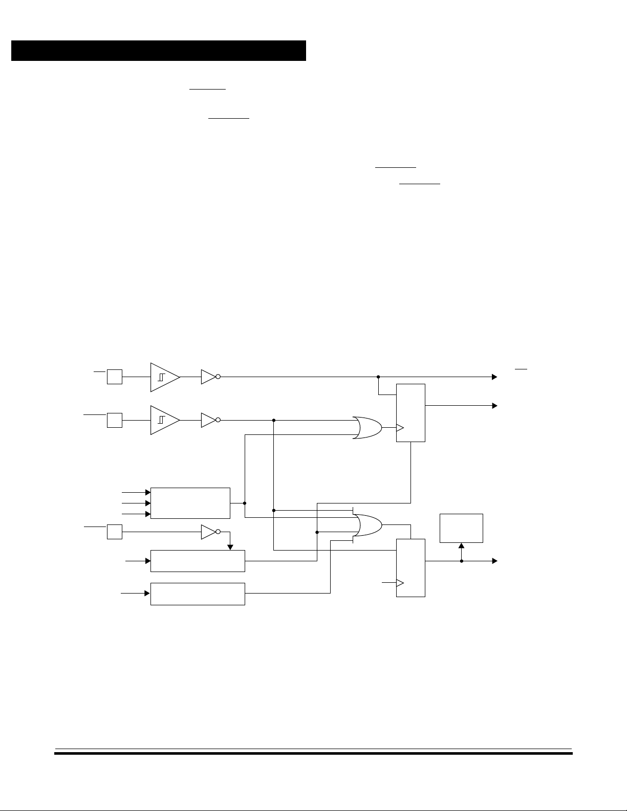
4.6 Hardware Interrupts
All hardware interrupts except RESET are maskable by the I bit in the
CCR. If the I bit is set, all hardware interrupts (internal and external) are
disabled. Clearing the I bit enables the hardware interrupts. The three
types of hardware interrupts are explained in the following sections.
4.7 External Interrupt (IRQ/Port B Keyscan)
The IRQ pin provides an asynchronous interrupt to the CPU. A block
diagram of the IRQ function is shown in Figure 4-2.
Interrupts
Hardware Interrupts
NOTE:
EIMSK
IRQ PIN
PORT B KEYSCAN
INTERRUPT
IRQ VECTOR FETCH
RST
LEVEL
(MASK OPTION)
The BIH and BIL instructions will apply to the level on the IRQ pin itself
and to the output of the logic OR function with the port B IRQ interrupts.
The states of the individual port B pins can be checked by reading the
appropriate port B pins as inputs.
The IRQ pin is one source of an external interrupt. All port B pins
(PB0–PB7) act as other external interrupt sources if the pullup feature is
enabled as specified by the user.
TO BIH & BIL
V
DD
IRQ
LATCH
R
INSTRUCTION
SENSING
TO IRQ
PROCESSING
IN CPU
Figure 4-2. IRQ Function Block Diagram
MC68HC05RC16 — Rev. 3.0 General Release Specification
MOTOROLA Interrupts 41
Page 42

Interrupts
When edge sensitivity is selected for the IRQ interrupt, it is sensitive to
these cases:
1. Falling edge on the IRQ pin
2. Falling edge on any port B pin with pullup enabled
When edge and level sensitivity is selected for the IRQ interrupt, it is
sensitive to these cases:
1. Low level on the IRQ pin
2. Falling edge on the
3. Falling edge or low level on any port B pin with pullup enabled
External interrupts also can be masked by setting the EIMSK bit in the
MSCR register of the IR remote timer. See 9.5.4 Modulator Period
Data Registers (MDR1, MDR2, and MDR3) for details.
4.8 External Interrupt Timing
If the interrupt mask bit (I bit) of the CCR is set, all maskable interrupts
(internal and external) are disabled. Clearing the I bit enables interrupts.
The interrupt request is latched immediately following the falling edge of
the
IRQ source. It is then synchronized internally and serviced as
specified by the contents of $3FFA and $3FFB.
Either a level-sensitive and edge-sensitive trigger or an
edge-sensitive-only trigger is available via the mask programmable
option for the
IRQ pin
IRQ pin.
4.9 Carrier Modulator Transmitter Interrupt (CMT)
A CMT interrupt occurs when the end of cycle flag (EOC) and the end of
cycle interrupt enable (EOCIE) bits are set in the modulator control and
status register (MCSR). This interrupt will vector to the interrupt service
routine located at the address specified by the contents of memory
locations $3FF8 and $3FF9.
General Release Specification MC68HC05RC16 — Rev. 3.0
42 Interrupts MOTOROLA
Page 43

4.10 Core Timer Interrupt
This timer can create two types of interrupts. A timer overflow interrupt
occurs whenever the 8-bit timer rolls over from $FF to $00 and the
enable bit TOFE is set. A real-time interrupt occurs whenever the
programmed time elapses and the enable bit RTIE is set. Either of these
interrupts vectors to the same interrupt service routine, located at the
address specified by the contents of memory locations $3FF6 and
$3FF7.
Interrupts
Core Timer Interrupt
MC68HC05RC16 — Rev. 3.0 General Release Specification
MOTOROLA Interrupts 43
Page 44

Interrupts
General Release Specification MC68HC05RC16 — Rev. 3.0
44 Interrupts MOTOROLA
Page 45

General Release Specification — MC68HC05RC16
5.1 Contents
5.2 Introduction. . . . . . . . . . . . . . . . . . . . . . . . . . . . . . . . . . . . . . . .45
5.3 External Reset (RESET). . . . . . . . . . . . . . . . . . . . . . . . . . . . . .46
5.4 Low-Power External Reset (LPRST) . . . . . . . . . . . . . . . . . . . .48
5.5 Internal Resets . . . . . . . . . . . . . . . . . . . . . . . . . . . . . . . . . . . . .48
5.5.1 Power-On Reset (POR). . . . . . . . . . . . . . . . . . . . . . . . . . . .48
5.5.2 Computer Operating Properly Reset (COPR). . . . . . . . . . .49
5.5.2.1 Resetting the COP. . . . . . . . . . . . . . . . . . . . . . . . . . . . . .49
5.5.2.2 COP During Wait Mode . . . . . . . . . . . . . . . . . . . . . . . . . .49
5.5.2.3 COP During Stop Mode . . . . . . . . . . . . . . . . . . . . . . . . . .49
5.5.2.4 COP Watchdog Timer Considerations. . . . . . . . . . . . . . .50
5.5.2.5 COP Register. . . . . . . . . . . . . . . . . . . . . . . . . . . . . . . . . .51
5.5.3 Illegal Address. . . . . . . . . . . . . . . . . . . . . . . . . . . . . . . . . . .51
Section 5. Resets
5.2 Introduction
The MCU can be reset from five sources: two external inputs and three
internal restart conditions. The
shown in Figure 5-1. All the internal peripheral modules will be reset by
the internal reset signal (RST). Refer toFigure 5-2 for reset timing detail.
MC68HC05RC16 — Rev. 3.0 General Release Specification
MOTOROLA Resets 45
RESET and LPRST pins are inputs as
Page 46
Resets
5.3 External Reset (RESET)
The RESET pin is one of the two external sources of a reset. This pin is
connected to a Schmitt trigger input gate to provide an upper and lower
threshold voltage separated by a minimum amount of hysteresis. This
external reset occurs whenever the
threshold and remains in reset until the
upper threshold. This active-low input will generate the RST signal and
reset the CPU and peripherals. Termination of the external RESET input
or the internal COP watchdog reset are the only reset sources that can
alter the operating mode of the MCU.
RESET pin is pulled below the lower
RESET pin rises above the
IRQ
RESET
DATA
ADDRESS
LPRST
ADDRESS
OSC
V
DD
NOTE:
COP WATCHDOG
Activation of the RST signal is generally referred to as reset of the
device, unless otherwise specified.
D
LATCH
R
CLOCKED
(COPR)
CPU
S
POWER-ON RESET
(POR)
ILLEGAL ADDRESS
(ILLADDR)
PH2
D
LATCH
RST
TO
IRQ
LOGIC
MODE
SELECT
TO OTHER
PERIPHERALS
Figure 5-1. Reset Block Diagram
General Release Specification MC68HC05RC16 — Rev. 3.0
46 Resets MOTOROLA
Page 47
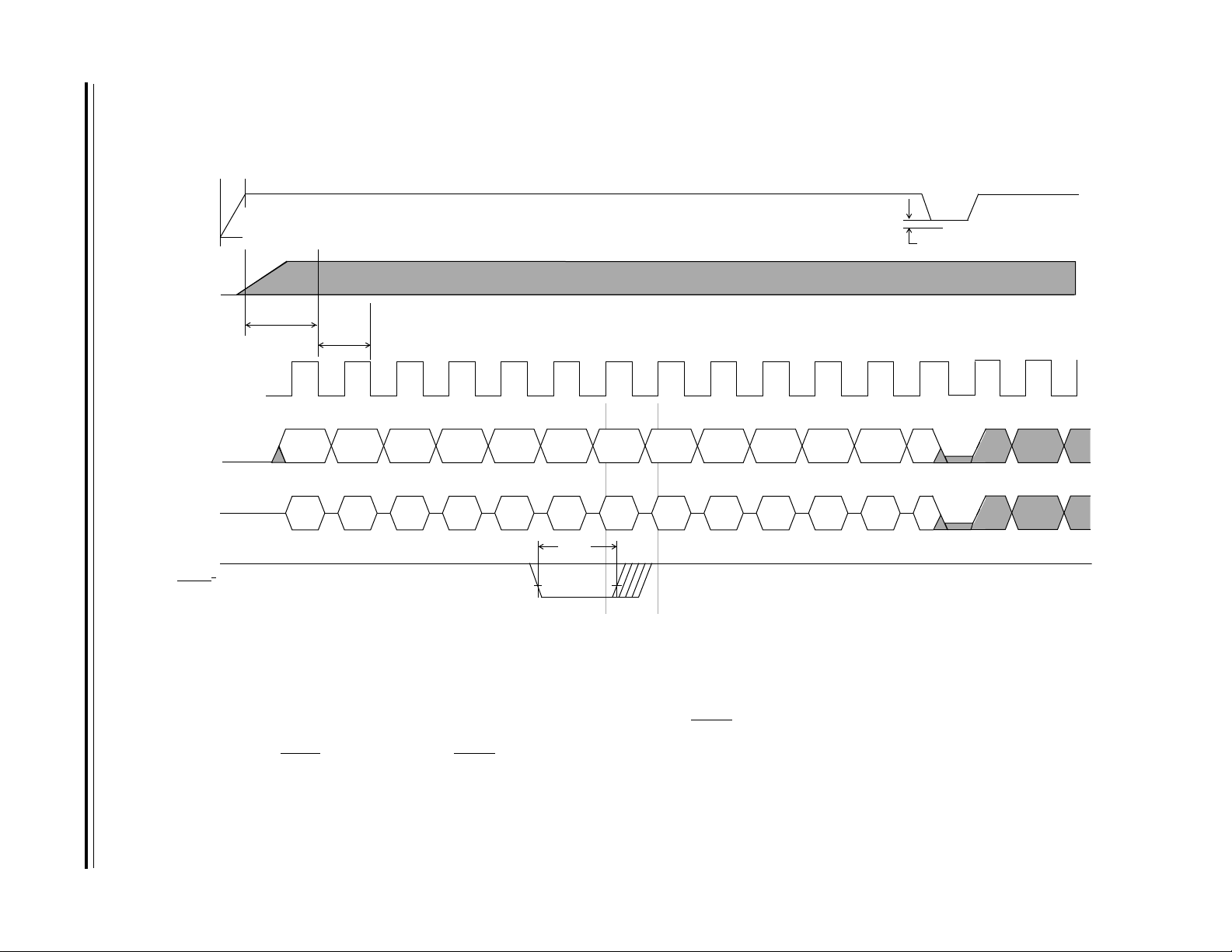
MC68HC05RC16 — Rev. 3.0 General Release Specification
MOTOROLA Resets 47
V
DD
2
OSC1
INTERNAL
PROCESSOR
CLOCK
INTERNAL
ADDRESS
BUS
1
1
0 V
4064 t
CYC
3FFE 3FFF
t
CYC
NEW PC NEW PC
3FFE3FFE3FFE 3FFE NEW PC3FFF
NEW PC
> V
POR
4
INTERNAL
DATA
BUS
RESET
1
5
NOTES:
1. Internal timing signal and bus information are not available externally.
2. OSC1 line is not meant to represent frequency. It is only used to represent time.
3. The next rising edge of the internal processor clock following the rising edge of RESET initiates the reset sequence.
4. VDD must fall to a level lower than V
5. The
NEW NEW OP
LPRST pin resets the CPU like RESET. However, 4064 POR cycles are executed first, before the reset vector address appears on the
internal address bus. (See 5.4 Low-Power External Reset (LPRST).)
CODEPCLPCH
t
RL
3
to be recognized as a power-on reset.
POR
PCH PCL
Figure 5-2. Reset and POR Timing Diagram
OP
CODE
External Reset (RESET)
Resets
Page 48

Resets
5.4 Low-Power External Reset (LPRST)
The LPRST pin is one of the two external sources of a reset. This
external reset occurs whenever the
threshold and remains in reset until the
input will, in addition to generating the RST signal and resetting the CPU
and peripherals, halt all internal processor clocks. The MCU will remain
in this low-power reset condition as long as a logic 0 remains on LPRST.
When a logic 1 is applied to LPRST , processor cloc ks will be re-enabled
with the MCU remaining in reset until the 4064 internal processor clock
cycle (t
) oscillator stabilization delay is completed. If any other reset
cyc
function is active at the end of this 4064-cycle delay, the RST signal
remains in the reset condition until the other reset condition(s) end.
5.5 Internal Resets
LPRST pin is pulled below the lower
LPRST pin rises. This active low
The three internally generated resets are the initial power-on reset
function, the COP watchdog timer reset, and the illegal address detector.
Termination of the external reset input, external
internal COP watchdog timer are the only reset sources that can alter the
operating mode of the MCU. The other internal resets do not have any
effect on the mode of operation when their reset state ends.
5.5.1 Power-On Reset (POR)
The internal POR is generated on power-up to allow the clock oscillator
to stabilize. The POR is strictly for power turn-on conditions and is not
able to detect a drop in the power supply voltage (brown-out). There is
an oscillator stabilization delay of 4064 internal processor bus clock
cycles (PH2) after the oscillator becomes active.
The POR generates the RST signal that resets the CPU. If any other
reset function is active at the end of this 4064-cycle delay, the RST
signal remains in the reset condition until the other reset condition(s)
ends.
LPRST input, or the
General Release Specification MC68HC05RC16 — Rev. 3.0
48 Resets MOTOROLA
Page 49

5.5.2 Computer Operating Properly Reset (COPR)
The MCU contains a watchdog timer that automatically times out if not
reset (cleared) within a specific time by a program reset sequence. If the
COP watchdog timer is allowed to time out, an internal reset is
generated to reset the MCU.
The COP reset function is enabled or disabled by a mask option and is
verified during production testing.
5.5.2.1 Resetting the COP
Writing a zero to the COPF bit prevents a COP reset. This action resets
the counter and begins the time-out period again. The COPF bit is bit 0
of address $3FF0. A read of address $3FF0 returns user data
programmed at that location.
Resets
Internal Resets
5.5.2.2 COP During Wait Mode
The COP continues to operate normally during wait mode. The software
should pull the device out of wait mode periodically and reset the COP
by writing to the COPF bit to prevent a COP reset.
5.5.2.3 COP During Stop Mode
When the stop enable mask option is selected, stop mode disables the
oscillator circuit and thereby turns the clock off for the entire device.
When stop is executed, the COP counter will hold its current state. If a
reset is used to exit stop mode, the COP counter is reset and held until
4064 POR cycles are completed at this time, counting will begin. If an
external IRQ is used to exit stop mode, the COP counter does not wait
for the completion of the 4064 POR cycles but does count these cycles.
It is, therefore, recommended that the COP is fed before executing the
STOP instruction.
MC68HC05RC16 — Rev. 3.0 General Release Specification
MOTOROLA Resets 49
Page 50

Resets
5.5.2.4 COP Watchdog Timer Considerations
The COP watchdog timer is active in all modes of operation if enabled
by a mask option. If the COP watchdog timer is selected by a mask
option, any execution of the STOP instruction (either intentionally or
inadvertently due to the CPU being disturbed) causes the oscillator to
halt and prevents the COP watchdog timer from timing out. If the COP
watchdog timer is selected by a mask option, the COP resets the MCU
when it times out. Therefore, it is recommended that the COP watchdog
be disabled for a system that must have intentional uses of the wait
mode for periods longer than the COP time out period.
The recommended interactions and considerations for the COP
watchdog timer, STOP instruction, and WAIT instruction are
summarized in Table 5-1.
Table 5-1. COP Watchdog Timer Recommendations
IF the Following Conditions Exist:
Wait Time
Wait Time Less than COP Time-Out Enable or Disable COP by Mask Option
Wait Time More than COP Time-Out Disable COP by Mask Option
Any Length Wait Time Disable COP by Mask Option
THEN the COP Watchdog Timer
Should Be as Follows:
General Release Specification MC68HC05RC16 — Rev. 3.0
50 Resets MOTOROLA
Page 51

5.5.2.5 COP Register
Resets
Internal Resets
The COP register is shared with the LSB of an unimplemented user
interrupt vector as shown in Figure 5-3. Reading this location returns
whatever user data has been programmed at this location. Writing a zero
to the COPR bit in this location clears the COP watchdog timer.
Address: $3FF0
BIt 7 654321Bit 0
Read: X X X X X X X X
Write: COPR
Reset: ———————0
= Unimplemented
Figure 5-3. COP Watchdog Timer Location
5.5.3 Illegal Address
An illegal address reset is generated when the CPU attempts to fetch an
instruction from I/O address space ($0000 to $001F).
MC68HC05RC16 — Rev. 3.0 General Release Specification
MOTOROLA Resets 51
Page 52

Resets
General Release Specification MC68HC05RC16 — Rev. 3.0
52 Resets MOTOROLA
Page 53

General Release Specification — MC68HC05RC16
Section 6. Low-Power Modes
6.1 Contents
6.2 Introduction. . . . . . . . . . . . . . . . . . . . . . . . . . . . . . . . . . . . . . . .53
6.3 Stop Mode . . . . . . . . . . . . . . . . . . . . . . . . . . . . . . . . . . . . . . . .53
6.4 Stop Recovery . . . . . . . . . . . . . . . . . . . . . . . . . . . . . . . . . . . . .54
6.5 Wait Mode. . . . . . . . . . . . . . . . . . . . . . . . . . . . . . . . . . . . . . . . .54
6.6 Low-Power Reset . . . . . . . . . . . . . . . . . . . . . . . . . . . . . . . . . . .55
6.2 Introduction
6.3 Stop Mode
NOTE:
This section describes the low-power modes.
The STOP instruction places the MCU in its lowest power-consumption
mode. In stop mode, the internal oscillator is turned off, halting all
internal processing, including timer operation.
During stop mode, the CTCSR ($08) bits are altered to remove any
pending timer interrupt request and to disable any further timer
interrupts. The timer prescaler is cleared. The I bit in the CCR is cleared
to enable external interrupts. All other registers and memory remain
unaltered. All input/output lines remain unchanged.
The EIMSK bit is not cleared automatically by the execution of a STOP
instruction. Care should be taken to clear this bit before entering stop
mode.
MC68HC05RC16 — Rev. 3.0 General Release Specification
MOTOROLA Low-Power Modes 53
Page 54

Low-Power Modes
OSC1
RESET
IRQ
1
t
RL
t
2
LIH
IRQ
INTERNAL
CLOCK
INTERNAL
ADDRESS
BUS
NOTES:
1. Represents the internal gating of the OSC1 pin
2. IRQ pin edge-sensitive mask option
3. IRQ pin level and edge-sensitive mask option
6.4 Stop Recovery
t
3
ILCH
4064 t
CYC
3FFE 3FFE 3FFE 3FFE 3FFF
RESET OR INTERRUPT
VECTOR FETCH
Figure 6-1. Stop Recovery Timing Diagram
The processor can be brought out of stop mode only by an external
interrupt,
LPRST, or RESET. Refer to Figure 6-1.
NOTE:
If an external interrupt is pending when stop mode is entered, then stop
mode will be exited immediately.
6.5 Wait Mode
The WAIT instruction places the MCU in a low power-consumption
mode, but wait mode consumes more power than stop mode. All CPU
action is suspended, but the core timer, the oscillator, and any enabled
module remain active. Any interrupt or reset will cause the MCU to exit
wait mode. The user must shut off subsystems to reduce power
General Release Specification MC68HC05RC16 — Rev. 3.0
54 Low-Power Modes MOTOROLA
Page 55

consumption. Wait current specifications assume CPU operation only
and do not include current consumption by any other subsystems.
During wait mode, the I bit in the CCR is cleared to enable interrupts. All
other registers, memory, and input/output lines remain in their previous
states. The timer may be enabled to allow a periodic exit from wait mode.
6.6 Low-Power Reset
Low-power reset mode is entered when a logic 0 is detected on the
LPRST pin. When in this mode (as long asLPRST is held low), the MCU
is held in reset and all internal clocks are halted. Applying a logic 1 to
LPRST will cause the part to exit low-power reset mode and begin
counting out the 4064-cycle oscillator stabilization period. Once this time
has elapsed, the MCU will begin operation from the reset vectors
($3FFE–$3FFF).
Low-Power Modes
Low-Power Reset
MC68HC05RC16 — Rev. 3.0 General Release Specification
MOTOROLA Low-Power Modes 55
Page 56

Low-Power Modes
EXTERNAL
INTERRUPT
(PTB KEYSCAN PULLUPS)
N
(IRQ)
STOP OSCILLATOR
AND ALL CLOCKS.
CLEAR I BIT.
N
Y
TURN ON OSCILLATOR.
WAIT FOR TIME
DELAY TO STABILIZE.
STOP
RESET
OR
LPRST
Y
WAIT
OSCILLATOR ACTIVE.
IR TIMER CLOCK ACTIVE.
CORE TIMER CLOCK ACTIVE.
PROCESSOR CLOCKS
STOPPED.
RESET
OR
LPRST
Y
RESTART
PROCESSOR CLOCK.
INTERRUPT
(PTB KEYSCAN PULLUPS)
N
EXTERNAL
IRQ)
(
Y
N
IR TIMER
INTERNAL
Y
INTERRUPT
Y
N
CORE TIMER
INTERNAL
INTERRUPT
N
1. FETCH RESET
VECTOR OR
2. SERVICE
INTERRUPT
A. STACK
B. SET I BIT
C. VECTOR TO
INTERRUPT
ROUTINE
Y
1. FETCH RESET
VECTOR OR
2. SERVICE
INTERRUPT
A. STACK
B. SET I BIT
C. VECTOR TO
INTERRUPT
ROUTINE
Figure 6-2. Stop/Wait Flowchart
General Release Specification MC68HC05RC16 — Rev. 3.0
56 Low-Power Modes MOTOROLA
Page 57

General Release Specification — MC68HC05RC16
Section 7. Parallel Input/Output (I/O)
7.1 Contents
7.2 Introduction. . . . . . . . . . . . . . . . . . . . . . . . . . . . . . . . . . . . . . . .57
7.3 Port A . . . . . . . . . . . . . . . . . . . . . . . . . . . . . . . . . . . . . . . . . . . .57
7.4 Port B . . . . . . . . . . . . . . . . . . . . . . . . . . . . . . . . . . . . . . . . . . . .58
7.5 Port C . . . . . . . . . . . . . . . . . . . . . . . . . . . . . . . . . . . . . . . . . . . .58
7.6 Input/Output Programming . . . . . . . . . . . . . . . . . . . . . . . . . . . .59
7.2 Introduction
7.3 Port A
NOTE:
In user mode, 20 lines (in 28-pin PDIP or SOIC) or 24 lines (in 44-lead
PLCC) are arranged as three 8-bit I/O ports. These ports are
programmable as either inputs or outputs under software control of the
data direction registers.
To avoid a glitch on the output pins, write data to the I/O port data
register before writing a one to the corresponding data direction register.
Port A is an 8-bit bidirectional port which does not share any of its pins
with other subsystems. The port A data register is at $0000 and the data
direction register (DDR) is at $0004. Reset does not affect the data
register, but clears the data direction register, thereby returning the ports
to inputs. Writing a one to a DDR bit sets the corresponding port bit to
output mode.
MC68HC05RC16 — Rev. 3.0 General Release Specification
MOTOROLA Parallel Input/Output (I/O) 57
Page 58

Parallel Input/Output (I/O)
7.4 Port B
Port B is an 8-bit bidirectional port which does not share any of its pins
with other subsystems. The address of the port B data register is $0001
and the data direction register (DDR) is at address $0005. Reset does
not affect the data register, but clears the data direction register, thereby
returning the ports to inputs. Writing a one to a DDR bit sets the
corresponding port bit to output mode. Each of the port B pins has a
mask programmable pullup device that can be enabled. When the pullup
device is enabled, this pin will become an interrupt pin also. The edge or
edge and level sensitivity of the
port B pins. Care needs to be taken when using port B pins that have the
pullup enabled. Before switching from an output to an input, the data
should be preconditioned to a logic one or the I bit should be set in the
condition code register to prevent an interrupt from occurring. The
EIMSK bit in the CMT MCSR register can be used to mask port B
keyscan and external interrupts (IRQ).
IRQ pin also will pertain to the enabled
7.5 Port C
NOTE:
When a port B pin is configured as an output, it’s corresponding keyscan
interrupt is disabled, regardless of it’s mask option.
PB7
V
DD
DISABLED
V
DD
MASK OPTION (PB7PU)
ENABLED
NORMAL PORT CIRCUITRY
AS SHOWN IN FIGURE 7-2
FROM ALL OTHER PORT B PINS
DDR BIT
IRQ
IRQEN
TO INTERRUPT
LOGIC
Figure 7-1. Port B Pullup Option
Port C is an 8-bit bidirectional port (PC0–PC7) which does not share any
of its pins with other subsystems. The port C data register is at $0003
and the data direction register (DDR) is at $0006. Reset does not affect
the data register, but clears the data direction register, thereby returning
General Release Specification MC68HC05RC16 — Rev. 3.0
58 Parallel Input/Output (I/O) MOTOROLA
Page 59

Parallel Input/Output (I/O)
Input/Output Programming
the ports to inputs. Writing a one to a DDR bit sets the corresponding
port bit to output mode. Port C pins PC4–PC7 are available only with the
44-lead PLCC package.
NOTE:
Only four bits of port C are bonded out in 28-pin packages for the
MC68HC05RC16, although port C is truly an 8-bit port. Since pins
PC4–PC7 are unbonded, software should include the code to set their
respective data direction register locations to outputs to avoid floating
inputs.
7.6 Input/Output Programming
Port pins may be programmed as inputs or outputs under software
control. The direction of the pins is determined by the state of the
corresponding bit in the port data direction register (DDR). Each I/O port
has an associated DDR. Any I/O port pin is configured as an output if its
corresponding DDR bit is set to a logic 1. A pin is configured as an input
if its corresponding DDR bit is cleared to a logic 0.
At power-on or reset, all DDRs are cleared, which configures all pins as
inputs. The data direction registers are capable of being written to or
read by the processor. During the programmed output state, a read of
the data register actually reads the value of the output data latch and not
the I/O pin.
Table 7-1. I/O Pin Functions
Access DDR I/O Pin Functions
Write 0
Write 1
Read 0 The state of the I/O pin is read.
Read 1 The I/O pin is in an output mode. The output data latch is read.
MC68HC05RC16 — Rev. 3.0 General Release Specification
MOTOROLA Parallel Input/Output (I/O) 59
The I/O pin is in input mode. Data is written into the output
data latch.
Data is written into the output data latch and output to the
I/O pin.
Page 60

Parallel Input/Output (I/O)
DATA DIRECTION
REGISTER BIT
INTERNAL
HC05
CONNECTIONS
LATCHED
OUTPUT
DATA BIT
INPUT
REG
BIT
Figure 7-2. I/O Circuitry
INPUT
I/O
OUTPUT
I/O
PIN
General Release Specification MC68HC05RC16 — Rev. 3.0
60 Parallel Input/Output (I/O) MOTOROLA
Page 61

General Release Specification — MC68HC05RC16
Section 8. Core Timer
8.1 Contents
8.2 Introduction. . . . . . . . . . . . . . . . . . . . . . . . . . . . . . . . . . . . . . . .61
8.3 Core Timer Control and Status Register. . . . . . . . . . . . . . . . . .63
8.4 Core Timer Counter Register . . . . . . . . . . . . . . . . . . . . . . . . . .65
8.5 Computer Operating Properly (COP) Reset. . . . . . . . . . . . . . .66
8.6 Timer During Wait Mode. . . . . . . . . . . . . . . . . . . . . . . . . . . . . .66
8.2 Introduction
The core timer for this device is a 14-stage multifunctional ripple counter.
Features include timer overflow, power-on reset (POR), real-time
interrupt (RTI), and COP watchdog timer.
As seen in Figure 8-1, the internal peripheral clock is divided by four,
and then drives an 8-bit ripple counter. The value of this 8-bit ripple
counter can be read by the CPU at any time by accessing the core timer
counter register (CTCR) at address $09. A timer overflow function is
implemented on the last stage of this counter, giving a possible interrupt
rate of the internal peripheral clock (E)/1024. This point is then followed
by three more stages, with the resulting clock (E/4096) driving the
real-time interrupt circuit (RTI). The RTI circuit consists of three divider
stages with a one-of-four selector. The output of the RTI circuit is further
divided by eight to drive the mask optional COP watchdog timer circuit.
The RTI rate selector bits and the RTI and CTOF enable bits and flags
are located in the timer control and status register at location $08.
MC68HC05RC16 — Rev. 3.0 General Release Specification
MOTOROLA Core Timer 61
Page 62

Core Timer
INTERNAL BUS
8
8
CTCR
CTCSR
$09 CORE TIMER COUNTER REGISTER (CTCR)
10
E ÷ 2
5-BIT COUNTER
E ÷ 215E ÷ 214E ÷ 213E ÷ 2
RTI SELECT CIRCUIT
OVERFLOW
DETECT
CIRCUIT
CTOF RTIF TOFE RTIE RT1
RTFCTOFC
INTERNAL PERIPHERAL CLOCK (E)
2
E ÷ 2
12
E ÷ 2
÷ 4
12
$08
RT0
TCBP
TIMER CONTROL &
STATUS REGISTER
RTI
POR
OUT
COP
CLEAR
INTERRUPT CIRCUIT
TO INTERRUPT
LOGIC
Figure 8-1. Core Timer Block Diagram
COP WATCHDOG
TIMER (÷8)
3
2
TO RESET
LOGIC
General Release Specification MC68HC05RC16 — Rev. 3.0
62 Core Timer MOTOROLA
Page 63

8.3 Core Timer Control and Status Register
The CTCSR contains the timer interrupt flag, the timer interrupt enable
bits, and the real-time interrupt rate select bits. Figure 8-2 shows the
value of each bit in the CTCSR when coming out of reset.
Address: $08
Core Timer
Core Timer Control and Status Register
Read: CTOF RTIF
TOFE RTIE
Write: TOFC RTFC
Reset: 00000011
= Unimplemented
00
RT1 RT0
Figure 8-2. Core Timer Control and Status Register (CTCSR)
CTOF — Core Timer Overflow
CTOF is a read-only status bit set when the 8-bit ripple counter rolls
over from $FF to $00. Clearing the CTOF is done by writing a one to
TOFC. Writing to this bit has no effect. Reset clears CTOF.
RTIF — Real-Time Interrupt Flag
The real-time interrupt circuit consists of a 3-stage divider and a
one-of-four selector. The clock frequency that drives the RTI circuit is
12
E/2
(or E ÷ 4096 with three additional divider stages giving a
maximum interrupt period of 16 milliseconds at a bus rate of 2.024
MHz. RTIF is a clearable, read-only status bit and is set when the
output of the chosen (one-of-four selection) stage goes active.
Clearing the RTIF is done by writing a one to RTFC. Writing has no
effect on this bit. Reset clears RTIF.
TOFE — Timer Overflow Enable
When this bit is set, a CPU interrupt request is generated when the
CTOF bit is set. Reset clears this bit.
RTIE — Real-Time Interrupt Enable
When this bit is set, a CPU interrupt request is generated when the
RTIF bit is set. Reset clears this bit.
MC68HC05RC16 — Rev. 3.0 General Release Specification
MOTOROLA Core Timer 63
Page 64

Core Timer
TOFC — Timer Overflow Flag Clear
When a one is written to this bit, CTOF is cleared. Writing a zero has
no effect on the CTOF bit. This bit always reads as zero.
RTFC — Real-Time Interrupt Flag Clear
When a one is written to this bit, RTIF is cleared. Writing a zero has
no effect on the RTIF bit. This bit always reads as zero.
RT1–RT0 — Real-Time Interrupt Rate Select
These two bits select one of four taps from the real-time interrupt
circuit. Refer toTable 8-1. Reset sets these two bits which selects the
lowest periodic rate and gives the maximum time in which to alter
these bits if necessary. Care should be taken when altering RT0 and
RT1 if the timeout period is imminent or uncertain. If the selected tap
is modified during a cycle in which the counter is switching, an RTIF
could be missed or an additional one could be generated. To avoid
problems, the COP should be cleared before changing RTI taps.
Table 8-1. RTI and COP Rates at 4.096 MHz Oscillator
RTI RATE
2.048-MHz Bus
2 ms
4 ms
8 ms
16 ms
212 ÷ E
213 ÷ E
214 ÷ E
215 ÷ E
RT1:RT0
00
01
10
11
MINIMUM COP RATES
2.048-MHz Bus
(215–212)/E
(216–213)/E
(217–214)/E
(218–215)/E
112 ms
14 ms
28 ms
56 ms
General Release Specification MC68HC05RC16 — Rev. 3.0
64 Core Timer MOTOROLA
Page 65

8.4 Core Timer Counter Register
The timer counter register is a read-only register that contains the
current value of the 8-bit ripple counter at the beginning of the timer
chain. This counter is clocked by the CPU clock (E/4) and can be used
for various functions, including a software input capture. Extended time
periods can be attained using the TOF function to increment a temporary
RAM storage location, thereby simulating a 16-bit (or more) counter.
Address: $09
Read: D7 D6 D5 D4 D3 D2 D1 D0
Write:
Reset: 00000011
= Unimplemented
Core Timer
Core Timer Counter Register
Figure 8-3. Core Timer Counter Register (CTCR)
The power-on cycle clears the entire counter chain and begins clocking
the counter. After 4064 cycles, the power-on reset circuit is released,
which again clears the counter chain and allows the device to come out
of reset. At this point, if
up from zero and normal device operation begins. When
RESET is not asserted, the timer starts counting
RESET is
asserted any time during operation (other than POR and low-power
reset), the counter chain is cleared.
MC68HC05RC16 — Rev. 3.0 General Release Specification
MOTOROLA Core Timer 65
Page 66

Core Timer
8.5 Computer Operating Properly (COP) Reset
The COP watchdog timer function is implemented on this device by
using the output of the RTI circuit and further dividing it by eight. The
minimum COP reset rates are listed inTable 8-1. If the COP circuit times
out, an internal reset is generated and the normal reset vector is fetched.
Preventing a COP timeout, or clearing the COP is accomplished by
writing a zero to bit 0 of address $3FF0. When the COP is cleared, only
the final divide-by-eight stage (output of the RTI) is cleared.
If the COP watchdog timer is allowed to time out, an internal reset is
generated to reset the MCU.
The COP remains enabled after execution of the WAIT instruction and
all associated operations apply. If the STOP instruction is disabled,
execution of STOP instruction causes the CPU to execute a WAIT
instruction. In addition, the COP is prohibited from being held in reset.
This prevents a device lock-up condition.
This COP’s objective is to make it impossible for this device to become
stuck or locked-up and to be sure the COP is able to rescue the part from
any situation where it might entrap itself in abnormal or unintended
behavior. This function is a mask option.
8.6 Timer During Wait Mode
The CPU clock halts during wait mode, but the timer remains active. If
interrupts are enabled, a timer interrupt will cause the processor to exit
wait mode. The COP is always enabled while in user mode.
General Release Specification MC68HC05RC16 — Rev. 3.0
66 Core Timer MOTOROLA
Page 67

General Release Specification — MC68HC05RC16
Section 9. Carrier Modulator Transmitter (CMT)
9.1 Contents
9.2 Introduction. . . . . . . . . . . . . . . . . . . . . . . . . . . . . . . . . . . . . . . .67
9.3 Overview. . . . . . . . . . . . . . . . . . . . . . . . . . . . . . . . . . . . . . . . . .68
9.4 Carrier Generator . . . . . . . . . . . . . . . . . . . . . . . . . . . . . . . . . . .70
9.4.1 Time Counter. . . . . . . . . . . . . . . . . . . . . . . . . . . . . . . . . . . .71
9.4.2 Carrier Generator Data Registers (CHR1, CLR1,
CHR2, and CLR2) . . . . . . . . . . . . . . . . . . . . . . . . . . . . .72
9.5 Modulator . . . . . . . . . . . . . . . . . . . . . . . . . . . . . . . . . . . . . . . . .74
9.5.1 Time Mode . . . . . . . . . . . . . . . . . . . . . . . . . . . . . . . . . . . . .76
9.5.2 FSK Mode . . . . . . . . . . . . . . . . . . . . . . . . . . . . . . . . . . . . . .77
9.5.3 Extended Space Operation. . . . . . . . . . . . . . . . . . . . . . . . .78
9.5.3.1 End Of Cycle (EOC) Interrupt . . . . . . . . . . . . . . . . . . . . .79
9.5.3.2 Modulator Control and Status Register (MCSR) . . . . . . .80
9.5.4 Modulator Period Data Registers
(MDR1, MDR2, and MDR3) . . . . . . . . . . . . . . . . . . . . . .83
9.2 Introduction
The carrier modulator transmitter (CMT) module provides a means to
generate the protocol timing and carrier signals for a wide variety of
encoding schemes. It incorporates hardware to off-load the critical
and/or lengthy timing requirements associated with code generation
from the CPU, releasing much of its bandwidth to handle other tasks
such as code data generation, data decompression, or keyboard
scanning. The CMT does not include dedicated hardware configurations
for specific protocols, but is intended to be sufficiently programmable in
its function to handle the timing requirements of most protocols with
minimal CPU intervention. When disabled, certain CMT registers can be
MC68HC05RC16 — Rev. 3.0 General Release Specification
MOTOROLA Carrier Modulator Transmitter (CMT) 67
Page 68

Carrier Modulator Transmitter (CMT)
used to change the state of the infrared out pin (IRO) directly. This
feature allows for the generation of future protocols not readily
producible by the current architecture.
9.3 Overview
The module consists of carrier generator, modulator, and transmitter
output blocks. The block diagram is shown in Figure 9-1.
The carrier generator has a resolution of 500 ns with a 2-MHz oscillator.
The user may independently define the high and low times of the carrier
signal to determine both period and duty cycle. The carrier generator can
generate signals with periods between 1 µs (1 MHz) and 64 µs (15.6
kHz) in steps of 500 ns. The possible duty cycle options will depend
upon the number of counts required to complete the carrier period. For
example, a 400-kHz signal has a period of 2.5 µs and will therefore
require 5 x 500 ns counts to generate. These counts may be split
between high and low times so the duty cycles available will be 20% (one
high, four low), 40% (two high, three low), 60% (three high, two low) and
80% (four high, one low). For lower frequency signals with larger
periods, higher resolution (as a percentage of the total period) duty
cycles are possible. The carrier generator may select between two sets
of high and low times. When operating in normal mode (subsequently
referred to as time mode), just one set will be used. When operating in
FSK (frequency shift key) mode, the generator will toggle between the
two sets when instructed to do so by the modulator, allowing the user to
dynamically switch between two carrier frequencies without CPU
intervention. When the BASE bit in the modulator control and status
register (MCSR) is set, the carrier output to the modulator is held high
continuously to allow for the generation of baseband protocols. See 9.4
Carrier Generator.
General Release Specification MC68HC05RC16 — Rev. 3.0
68 Carrier Modulator Transmitter (CMT) MOTOROLA
Page 69

PRIMARY/SECONDARY SELECT
MODE
BASE
Carrier Modulator Transmitter (CMT)
Overview
EOC
INTERRUPT
MODULATOR
MODULATOR/
CARRIER
ENABLE
ENABLE
OUT
TRANSMITTER
OUTPUT
f
OSC
f
OSC
÷ 2
CARRIER
.
GENERATOR
DB AB EOC INTERRUPT
CARRIER
OUT
MODULATOR
EOC FLAG
CPU INTERFACE
Figure 9-1. Carrier Modulator Transmitter Module Block Diagram
The modulator provides a simple method to control protocol timing. The
modulator has a resolution of 4 µs with a 2-MHz oscillator. It can count
system clocks to provide real-time control or it can count carrier clocks
for self-clocked protocols. It can either gate the carrier onto the
modulator output (TIME), control the logic level of the modulator output
(baseband) or directly route the carrier to the modulator output while
providing a signal to switch the carrier generator between high/low time
register buffers (FSK). See 9.5 Modulator.
IRO
PIN
The transmitter output block controls the state of the infrared out pin
(IRO). The modulator output is gated on to the IRO pin when the
modulator/carrier generator is enabled. Otherwise, the IRO pin is
controlled by the state of the IRO latch, which is directly accessible to the
CPU by means of bit 7 of the carrier generator data registers CHR1 and
CLR1. The IRO latch can be written to on either edge of the internal bus
clock (f
the bus clock frequency (f
/2), allowing for IR waveforms which have a resolution of twice
osc
). See 9.4.2 Carrier Generator Data
osc
Registers (CHR1, CLR1, CHR2, and CLR2).
MC68HC05RC16 — Rev. 3.0 General Release Specification
MOTOROLA Carrier Modulator Transmitter (CMT) 69
Page 70

Carrier Modulator Transmitter (CMT)
9.4 Carrier Generator
The carrier signal is generated by counting a predetermined number of
input clocks (500 ns for a 2-MHz oscillator) for both the carrier high time
and the carrier low time. The period is determined by the total number of
clocks counted. The duty cycle is determined by the ratio of high time
clocks to total clocks counted. The high and low time values are user
programmable and are held in two registers. An alternate set of high/low
count values is held in another set of registers to allow the generation of
dual frequency FSK (frequency shift keying) protocols without CPU
intervention. The MCGEN bit in the MCSR must be set and the BASE bit
in the MCSR must be cleared to enable carrier generator clocks. The
block diagram is shown in Figure 9-2.
f
OSC
BASE
MODULATOR/
CARRIER GENERATOR
ENABLE
CARRIER OUT
SECONDARY HIGH COUNT REGISTER
PRIMARY HIGH COUNT REGISTER
=?
CLK
6-BIT UP COUNTER
CLR
CLOCK AND OUTPUT CONTROL
=?
SECONDARY LOW COUNT REGISTER
PRIMARY LOW COUNT REGISTER
Figure 9-2. Carrier Generator Block Diagram
MODE
PRIMARY/
SECONDARY
SELECT
COUNT REGISTER SELECT CONTROL
General Release Specification MC68HC05RC16 — Rev. 3.0
70 Carrier Modulator Transmitter (CMT) MOTOROLA
Page 71

9.4.1 Time Counter
Carrier Modulator Transmitter (CMT)
Carrier Generator
The high/low time counter is a 6-bit up counter. After each increment, the
contents of the counter are compared with the appropriate high or low
count value register. When this value is reached, the counter is reset and
the compare is redirected to the other count value register. Assuming
that the high time count compare register is currently active, a valid
compare will cause the carrier output to be driven low. The counter will
continue to increment and when reaching the value stored in the
selected low count value register, it will be cleared and will cause the
carrier output to be driven high. The cycle repeats, automatically
generating a periodic signal which is directed to the modulator. The
lowest frequency (maximum period) and highest frequency (minimum
period) which can be generated are defined below.
f
min
= f
÷ (2 x (26 – 1)) Hz
osc
NOTE:
f
max
= f
÷ (2 x 1) Hz
osc
In the general case, the carrier generator output frequency is:
f
out
= f
÷ (Highcount + Lowcount) Hz
osc
Where:
0 <
Highcount
0 <
Lowcount
< 64 and
< 64
These equations assume the DIV2 bit (bit 6) of the MCSR is clear. When
the DIV2 bit is set, the carrier generator frequency will be half of what is
shown in these equations.
The duty cycle of the carrier signal is controlled by varying the ratio of
high time to low + high time. As the input clock period is fixed, the duty
cycle resolution will be proportional to the number of counts required to
generate the desired carrier period.
DutyCycle
Highcount
----------------------------------------------------------------=
Highcount Lowcount+
MC68HC05RC16 — Rev. 3.0 General Release Specification
MOTOROLA Carrier Modulator Transmitter (CMT) 71
Page 72

Carrier Modulator Transmitter (CMT)
9.4.2 Carrier Generator Data Registers (CHR1, CLR1, CHR2, and CLR2)
The carrier generator contains two, 7-bit data registers: primary high
time (CHR1), primary low time (CLR1); and two, 6-bit data registers:
secondary high time (CHR2) and secondary low time (CLR2). Bit 7 of
CHR1 and CHR2 is used to read and write the IRO latch.
Address: $0010
Bit 7 654321Bit 0
Read:
IROLN 0 PH5 PH4 PH3 PH2 PH1 PH0
Write:
Reset: 0 0 UUUUUU
U = Unaffected
Figure 9-3. Carrier Generator Data Register CHR1
Address: $0011
Bit 7 654321Bit 0
Read:
IROLP 0 PL5 PL4 PL3 PL2 PL1 PL0
Write:
Reset: 0 0 UUUUUU
U = Unaffected
Figure 9-4. Carrier Generator Data Register CLR1
Address: $0012
Bit 7 654321Bit 0
Read:
0 0 SH5 SH4 SH3 SH2 SH1 SH0
Write:
Reset: 0 0 UUUUUU
U = Unaffected
Figure 9-5. Carrier Generator Data Register CHR2
General Release Specification MC68HC05RC16 — Rev. 3.0
72 Carrier Modulator Transmitter (CMT) MOTOROLA
Page 73

Carrier Modulator Transmitter (CMT)
Carrier Generator
Address: $0013
Bit 7 654321Bit 0
Read:
0 0 SL5 SL4 SL3 SL2 SL1 SL0
Write:
Reset: 0 0 UUUUUU
U = Unaffected
Figure 9-6. Carrier Generator Data Register CLR2
PH0–PH5 and PL0–PL5 — Primary Carrier High and Low Time Data
Values
When selected, these bits contain the number of input clocks required
to generate the carrier high and low time periods. When operating in
time mode (see 9.5.1 Time Mode), this register pair is always
selected. When operating in FSK mode (see 9.5.2 FSK Mode), this
register pair and the secondary register pair are alternately selected
under control of the modulator. The primary carrier high and low time
values are undefined out of reset. These bits must be written to
nonzero values before the carrier generator is enabled to avoid
spurious results.
NOTE:
Writing to CHR1 to update PH0–PH5 or to CLR1 to update PL0–PL5 will
also update the IRO latch. When MCGEN (bit 0 in the MCSR) is clear,
the IRO latch value appears on the IRO output pin. Care should be taken
that bit 7 of the data to be written to CHR1 or CHL1 should contain the
desired state of the IRO latch.
SH0–SH5 and SL0–SL5 — Secondary Carrier High and Low Time Data
Values
When selected, these bits contain the number of input clocks required
to generate the carrier high and low time periods. When operating in
time mode (see9.5.1 Time Mode), this register pair is never selected.
When operating in FSK mode (see9.5.2 FSK Mode), this register pair
and the secondary register pair are alternately selected under control
MC68HC05RC16 — Rev. 3.0 General Release Specification
MOTOROLA Carrier Modulator Transmitter (CMT) 73
Page 74

Carrier Modulator Transmitter (CMT)
of the modulator. The secondary carrier high and low time values are
undefined out of reset. These bits must be written to nonzero values
before the carrier generator is enabled when operating in FSK mode.
IROLN and IROLP — IRO Latch Control
Reading IROLN or IROLP reads the state of the IRO latch. Writing
IROLN updates the IRO latch with the data being written on the
negative edge of the internal processor clock (f
updates the IRO latch on the positive edge of the internal processor
clock; for example, one f
reset.
/2). Writing IROLP
osc
period later. The IRO latch is clear out of
osc
NOTE:
9.5 Modulator
Writing to CHR1 to update IROLN or to CLR1 to update IROLP will also
update the primary carrier high and low data values. Care should be
taken that bits 5–0 of the data to be written to CHR1 or CHL1 should
contain the desired values for the primary carrier high or low data.
The modulator consists of a 12-bit down counter with underflow
detection which is loaded from the modulation mark period from the
mark buffer register, MBUFF. When this counter underflows, the
modulator gate is closed and a 12-bit comparator is enabled which
continually compares the logical complement of the contents of the (still)
decrementing counter with the contents of the modulation space period
register, SREG. When a match is obtained, the modulator control gate
is opened again. Should SREG = 0, the match will be immediate and no
space period will be generated (for instance, for FSK protocols which
require successive bursts of different frequencies). When the match
occurs, the counter is reloaded with the contents of MBUFF, SREG is
reloaded with the contents of its buffer, SBUFF, and the cycle repeats.
The MCGEN bit in the MCSR must be set to enable the modulator timer.
The 12-bit MBUFF and SBUFF registers are accessed through three
8-bit modulator period registers, MDR1, MDR2, and MDR3.
General Release Specification MC68HC05RC16 — Rev. 3.0
74 Carrier Modulator Transmitter (CMT) MOTOROLA
Page 75

Carrier Modulator Transmitter (CMT)
Modulator
The modulator can operate in two modes, time or FSK. In time mode the
modulator counts clocks derived from the system oscillator and
modulates a single-carrier frequency or no carrier (baseband). In FSK
mode, the modulator counts carrier periods and instructs the carrier
generator to alternate between two carrier frequencies whenever a
modulation period (mark + space counts) expires.
12 BITS
0
MS BIT
* DENOTES HIDDEN REGISTER
MBUFF
13-BIT DOWN COUNTER *
COUNTER
=?
SREG *
SBUFF
12 BITS
8
CLOCK CONTROL
12
LOAD MBUFF/SBUFF
.
SYSTEM CONTROL
12
MODULATOR
CONTROL/STATUS REGISTER
MODULATOR GATE
EOC FLAG SET
EXTENDED SPACE
.
PRIMARY/SECONDARY SELECT
f
OSC
CARRIER OUT
MODULATOR
OUT
MODULATOR/
CARRIER GENERATOR.
ENABLE
EOC FLAG
EOC INTERRUPT ENABLE
MODE
BASE
DIV2
Figure 9-7. Modulator Block Diagram
MC68HC05RC16 — Rev. 3.0 General Release Specification
MOTOROLA Carrier Modulator Transmitter (CMT) 75
Page 76

Carrier Modulator Transmitter (CMT)
9.5.1 Time Mode
When the modulator operates in time mode, the modulation mark and
space periods consist of zero or an integer number of f
(= 250 kHz @ 2 MHz osc). This provides a modulator resolution of 4 µs
and a maximum mark and space periods of about 16 ms (each).
However, to prevent carrier glitches which could affect carrier spectral
purity, the modulator control gate and carrier clock are synchronized.
The carrier signal is activated when the modulator gate opens. The
modulator gate can only close when the carrier signal is low (the output
logic level during space periods is low). If the carrier generator is in
baseband mode (BASE bit in MCSR is high), the modulator output will
be at a logic one for the duration of the mark period and at a logic zero
for the duration of a space period. See Figure 9-8.
The mark and space time equations are:
÷ 8 clocks
osc
t
mark
t
space
MBUFF 1+()8×
--------------------------------------------- -ssec=
f
osc
SBUFF 8×
------------------------------ ssec=
f
osc
Setting the DIV2 bit in the MCSR will double mark and space times.
General Release Specification MC68HC05RC16 — Rev. 3.0
76 Carrier Modulator Transmitter (CMT) MOTOROLA
Page 77

f
÷ 8
OSC
CARRIER FREQUENCY
Carrier Modulator Transmitter (CMT)
Modulator
MODULATOR GATE
TIME MODE OUTPUT
BASEBAND OUTPUT
9.5.2 FSK Mode
MARK SPACE MARK MARKSPACE
Figure 9-8. CMT Operation in Time Mode
When the modulator operates in FSK mode, the modulation mark and
space periods consist of an integer number of carrier clocks (space
period can be zero). When the mark period expires, the space period is
transparently started (as in time mode); however, in FSK mode the
carrier switches between data registers in preparation for the next mark
period. The carrier generator toggles between primary and secondary
data register values whenever the modulator mark period expires. The
space period provides an interpulse gap (no carrier), but if SBUFF = 0,
then the modulator and carrier generator will switch between carrier
frequencies without a gap or any carrier glitches (zero space).
Using timing data for carrier burst and interpulse gap length calculated
by the CPU, FSK mode can automatically generate a phase-coherent,
dual-frequency FSK signal with programmable burst and interburst
gaps.
MC68HC05RC16 — Rev. 3.0 General Release Specification
MOTOROLA Carrier Modulator Transmitter (CMT) 77
Page 78

Carrier Modulator Transmitter (CMT)
The mark and space time equations for FSK mode are:
Where f
is the frequency output from the carrier generator, setting the
cg
DIV2 bit in the MCSR will double mark and space times.
9.5.3 Extended Space Operation
In either time or FSK mode, the space period can be made longer than
the maximum possible value of SBUFF. Setting the EXSPC bit in the
MCSR will force the modulator to treat the next modulation period
(beginning with the next load of MBUFF/SBUFF) as a space period
equal in length to the mark and space counts combined. Subsequent
modulation periods will consist entirely of these extended space periods
with no mark periods. Clearing EXSPC will return the modulator to
standard operation at the beginning of the next modulation period. To
calculate the length of an extended space in time mode, use the
equation:
t
mark
t
space
MBUFF 1+
------------------------------- ssec=
f
g
c
SBUFF
-------------------- -ssec=
f
cg
t
exspace
((SBUFF1)+(MBUFF2+1+SBUFF2) +... (MBUFFn+1+SBUFFn)) x 8
=
f
osc
secs
Where:
the subscripts 1, 2, ... n refer to the modulation periods that elapsed
while the EXSPC bit was set.
Similarly, to calculate the length of an extended space in FSK mode, use
the equation:
t
exspace
General Release Specification MC68HC05RC16 — Rev. 3.0
78 Carrier Modulator Transmitter (CMT) MOTOROLA
((SBUFF1)+(MBUFF2+1+SBUFF2)+... (MBUFFn+1+SBUFFn))
=
f
cg
secs
Page 79

Carrier Modulator Transmitter (CMT)
Modulator
Where fcg is the frequency output from the carrier generator. For an
example of extended space operation, see Figure 9-9.
NOTE:
The EXSPC feature can be used to emulate a zero mark event.
SET EXSPC
9.5.3.1 End Of Cycle (EOC) Interrupt
At the end of each cycle (when the counter is reloaded from MBUFF),
the end of cycle (EOC) flag is set. If the interrupt enable bit was
previously set, an interrupt also will be issued to the CPU. The EOC
interrupt provides a means for the user to reload new mark/space values
into the MBUFF and SBUFF registers. As the EOC interrupt is coincident
with reloading the counter, MBUFF does not require additional buffering
and may be updated with a new value for the next period from within the
EOC interrupt service routine (ISR). To allow both mark and space
period values to be updated from within the same ISR, SREG is buffered
by SBUFF. The contents written to SBUFF are transferred to the active
register SREG at the end of every cycle regardless of the state of the
EOC flag. The EOC flag is cleared by a read of the modulator control and
status register (MCSR) followed by an access of MDR2 or MDR3. The
EOC flag must be cleared within the ISR to prevent another interrupt
being generated after exiting the ISR. If the EOC interrupt is not being
used (IE = 0), the EOC flag need not be cleared.
CLEAR EXSPC
Figure 9-9. Extended Space Operation
MC68HC05RC16 — Rev. 3.0 General Release Specification
MOTOROLA Carrier Modulator Transmitter (CMT) 79
Page 80

Carrier Modulator Transmitter (CMT)
9.5.3.2 Modulator Control and Status Register
The modulator control and status register (MCSR) contains the
modulator and carrier generator enable (MCGEN), interrupt enable (IE),
mode select (MODE), baseband enable (BASE), extended space
(EXSPC), and external interrupt mask (EIMSK) control bits,
divide-by-two prescaler (DIV2) bit, and the end of cycle (EOC) status
bit.
Address: $0014
Bit 7 654321Bit 0
Read: EOC
DIV2 EIMSK EXSPC BASE MODE IE MCGEN
Write:
Reset: 00000000
Unimplemented
Figure 9-10. Modulator Control and Status Register (MCSR)
EOC — End Of Cycle Status Flag
EOC is set when a match occurs between the contents of the space
period register, SREG, and the down counter. This is recognized as
the end of the modulation cycle. At this time, the counter is initialized
with the (possibly new) contents of the mark period buffer, MBUFF,
and the space period register, SREG, is loaded with the (possibly
new) contents of the space period buffer, SBUFF. This flag is cleared
by a read of the MCSR followed by an access of MDR2 or MDR3. The
EOC flag is cleared by reset.
1 = End of modulator cycle (counter = SBUFF) has occurred
0 = Current modulation cycle in progress
DIV2 — Divide-by-two prescaler
The divide-by-two prescaler causes the CMT to be clocked at the bus
rate when enabled; 2 x the bus rate when disabled (f
). This bit is
osc
not double buffered and so should not be set during a transmission.
1 = Divide-by-two prescaler enabled
0 = Divide-by-two prescaler disabled
General Release Specification MC68HC05RC16 — Rev. 3.0
80 Carrier Modulator Transmitter (CMT) MOTOROLA
Page 81

Carrier Modulator Transmitter (CMT)
Modulator
EIMSK — External Interrupt Mask
The external interrupt mask bit is used to mask IRQ and keyscan
interrupts. This bit is cleared by reset.
1 = IRQ and keyscan interrupts masked
0 = IRQ and keyscan interrupts enabled
EXSPC — Extended Space Enable
For a description of the extended space enable bit, see 9.5.3
Extended Space Operation. This bit is cleared by reset.
1 = Extended space enabled
0 = Extended space disabled
BASE — Baseband Enable
When set, the BASE bit disables the carrier generator and forces the
carrier output high for generation of baseband protocols. When BASE
is clear, the carrier generator is enabled and the carrier output toggles
at the frequency determined by values stored in the carrier data
registers. See 9.5.1 Time Mode. This bit is cleared by reset. This bit
is not double buffered and should not be written to during a
transmission.
1 = Baseband enabled
0 = Baseband disabled
MODE — Mode Select
For a description of CMT operation in time mode, see 9.5.1 Time
Mode. For a description of CMT operation in FSK mode, see 9.5.2
FSK Mode. This bit is cleared by reset. This bit is not double buffered
and should not be written to during a transmission.
1 = CMT operates in FSK mode.
0 = CMT operates in time mode.
IE — Interrupt Enable
A CPU interrupt will be requested when EOC is set if IE was
previously set. If IE is clear, EOC will not request a CPU interrupt.
1 = CPU interrupt enabled
0 = CPU interrupt disabled
MC68HC05RC16 — Rev. 3.0 General Release Specification
MOTOROLA Carrier Modulator Transmitter (CMT) 81
Page 82

Carrier Modulator Transmitter (CMT)
MCGEN — Modulator and Carrier Generator Enable
Setting MCGEN will initialize the carrier generator and modulator and
will enable all clocks. Once enabled, the carrier generator and
modulator will function continuously. When MCGEN is cleared, the
current modulator cycle will be allowed to expire before all carrier and
modulator clocks are disabled (to save power) and the modulator
output is forced low. The user should initialize all data and control
registers before enabling the system to prevent spurious operation.
This bit is cleared by reset.
1 = Modulator and carrier generator enabled
0 = Modulator and carrier generator disabled
General Release Specification MC68HC05RC16 — Rev. 3.0
82 Carrier Modulator Transmitter (CMT) MOTOROLA
Page 83

Carrier Modulator Transmitter (CMT)
9.5.4 Modulator Period Data Registers (MDR1, MDR2, and MDR3)
The 12-bit MBUFF and SBUFF registers are accessed through three
8-bit registers: MDR1, MDR2, and MDR3. MDR2 and MDR3 contain the
least significant eight bits of MBUFF and SBUFF respectively. MDR1
contains the two most significant nibbles of MBUFF and SBUFF. In
many applications, periods greater than those obtained by eight bits will
not be required. Dividing the registers in this manner allows the user to
clear MDR1 and generate 8-bit periods with just two data writes.
Address: $0015
Bit 7 654321Bit 0
Read:
MB11 MB10 MB9 MB8 SB11 SB10 SB9 SB8
Write:
Reset: Unaffected by Reset
Modulator
Figure 9-11. Modulator Period Data Register MDR1
Address: $0016
Bit 7 654321Bit 0
Read:
MB7 MB6 MB5 MB4 MB3 MB2 MB1 MB0
Write:
Reset: Unaffected by Reset
Figure 9-12. Modulator Period Data Register MDR2
Address: $0017
Bit 7 654321Bit 0
Read:
SB7 SB6 SB5 SB4 SB3 SB2 SB1 SB0
Write:
Reset: Unaffected by Reset
Figure 9-13. Modulator Period Data Register MDR3
MC68HC05RC16 — Rev. 3.0 General Release Specification
MOTOROLA Carrier Modulator Transmitter (CMT) 83
Page 84

Carrier Modulator Transmitter (CMT)
General Release Specification MC68HC05RC16 — Rev. 3.0
84 Carrier Modulator Transmitter (CMT) MOTOROLA
Page 85

General Release Specification — MC68HC05RC16
Section 10. Instruction Set
10.1 Contents
10.2 Introduction. . . . . . . . . . . . . . . . . . . . . . . . . . . . . . . . . . . . . . . .86
10.3 Addressing Modes . . . . . . . . . . . . . . . . . . . . . . . . . . . . . . . . . .86
10.3.1 Inherent. . . . . . . . . . . . . . . . . . . . . . . . . . . . . . . . . . . . . . . .87
10.3.2 Immediate . . . . . . . . . . . . . . . . . . . . . . . . . . . . . . . . . . . . . .87
10.3.3 Direct. . . . . . . . . . . . . . . . . . . . . . . . . . . . . . . . . . . . . . . . . .87
10.3.4 Extended. . . . . . . . . . . . . . . . . . . . . . . . . . . . . . . . . . . . . . .87
10.3.5 Indexed, No Offset . . . . . . . . . . . . . . . . . . . . . . . . . . . . . . .88
10.3.6 Indexed, 8-Bit Offset . . . . . . . . . . . . . . . . . . . . . . . . . . . . . .88
10.3.7 Indexed,16-Bit Offset. . . . . . . . . . . . . . . . . . . . . . . . . . . . . .88
10.3.8 Relative . . . . . . . . . . . . . . . . . . . . . . . . . . . . . . . . . . . . . . . .89
10.4 Instruction Types . . . . . . . . . . . . . . . . . . . . . . . . . . . . . . . . . . .89
10.4.1 Register/Memory Instructions . . . . . . . . . . . . . . . . . . . . . . .90
10.4.2 Read-Modify-Write Instructions. . . . . . . . . . . . . . . . . . . . . .91
10.4.3 Jump/Branch Instructions . . . . . . . . . . . . . . . . . . . . . . . . . .92
10.4.4 Bit Manipulation Instructions . . . . . . . . . . . . . . . . . . . . . . . .94
10.4.5 Control Instructions . . . . . . . . . . . . . . . . . . . . . . . . . . . . . . .95
10.5 Instruction Set Summary . . . . . . . . . . . . . . . . . . . . . . . . . . . . .96
MC68HC05RC16 — Rev. 3.0 General Release Specification
MOTOROLA Instruction Set 85
Page 86

Instruction Set
10.2 Introduction
The MCU instruction set has 62 instructions and uses eight addressing
modes. The instructions include all those of the M146805 CMOS Family
plus one more: the unsigned multiply (MUL) instruction. The MUL
instruction allows unsigned multiplication of the contents of the
accumulator (A) and the index register (X). The high-order product is
stored in the index register, and the low-order product is stored in the
accumulator.
10.3 Addressing Modes
The CPU uses eight addressing modes for flexibility in accessing data.
The addressing modes provide eight different ways for the CPU to find
the data required to execute an instruction. The eight addressing modes
are:
• Inherent
• Immediate
• Direct
• Extended
• Indexed, no offset
• Indexed, 8-bit offset
• Indexed, 16-bit offset
• Relative
General Release Specification MC68HC05RC16 — Rev. 3.0
86 Instruction Set MOTOROLA
Page 87

10.3.1 Inherent
10.3.2 Immediate
Instruction Set
Addressing Modes
Inherent instructions are those that have no operand, such as return
from interrupt (RTI) and stop (STOP). Some of the inherent instructions
act on data in the CPU registers, such as set carry flag (SEC) and
increment accumulator (INCA). Inherent instructions require no operand
address and are one byte long.
Immediate instructions are those that contain a value to be used in an
operation with the value in the accumulator or index register. Immediate
instructions require no operand address and are two bytes long. The
opcode is the first byte, and the immediate data value is the second byte.
10.3.3 Direct
10.3.4 Extended
Direct instructions can access any of the first 256 memory locations with
two bytes. The first byte is the opcode, and the second is the low byte of
the operand address. In direct addressing, the CPU automatically uses
$00 as the high byte of the operand address.
Extended instructions use three bytes and can access any address in
memory. The first byte is the opcode; the second and third bytes are the
high and low bytes of the operand address.
When using the Motorola assembler, the programmer does not need to
specify whether an instruction is direct or extended. The assembler
automatically selects the shortest form of the instruction.
MC68HC05RC16 — Rev. 3.0 General Release Specification
MOTOROLA Instruction Set 87
Page 88

Instruction Set
10.3.5 Indexed, No Offset
Indexed instructions with no offset are 1-byte instructions that can
access data with variable addresses within the first 256 memory
locations. The index register contains the low byte of the effective
address of the operand. The CPU automatically uses $00 as the high
byte, so these instructions can address locations $0000–$00FF.
Indexed, no offset instructions are often used to move a pointer through
a table or to hold the address of a frequently used RAM or I/O location.
10.3.6 Indexed, 8-Bit Offset
Indexed, 8-bit offset instructions are 2-byte instructions that can access
data with variable addresses within the first 511 memory locations. The
CPU adds the unsigned byte in the index register to the unsigned byte
following the opcode. The sum is the effective address of the operand.
These instructions can access locations $0000–$01FE.
Indexed 8-bit offset instructions are useful for selecting the kth element
in an n-element table. The table can begin anywhere within the first 256
memory locations and could extend as far as location 510 ($01FE). The
k value is typically in the index register, and the address of the beginning
of the table is in the byte following the opcode.
10.3.7 Indexed,16-Bit Offset
Indexed, 16-bit offset instructions are 3-byte instructions that can access
data with variable addresses at any location in memory. The CPU adds
the unsigned byte in the index register to the two unsigned bytes
following the opcode. The sum is the effective address of the operand.
The first byte after the opcode is the high byte of the 16-bit offset; the
second byte is the low byte of the offset.
Indexed, 16-bit offset instructions are useful for selecting the kth element
in an n-element table anywhere in memory.
As with direct and extended addressing, the Motorola assembler
determines the shortest form of indexed addressing.
General Release Specification MC68HC05RC16 — Rev. 3.0
88 Instruction Set MOTOROLA
Page 89

10.3.8 Relative
Relative addressing is only for branch instructions. If the branch
condition is true, the CPU finds the effective branch destination by
adding the signed byte following the opcode to the contents of the
program counter. If the branch condition is not true, the CPU goes to the
next instruction. The offset is a signed, two’s complement byte that gives
a branching range of –128 to +127 bytes from the address of the next
location after the branch instruction.
When using the Motorola assembler, the programmer does not need to
calculate the offset, because the assembler determines the proper offset
and verifies that it is within the span of the branch.
10.4 Instruction Types
Instruction Set
Instruction Types
The MCU instructions fall into the following five categories:
• Register/Memory Instructions
• Read-Modify-Write Instructions
• Jump/Branch Instructions
• Bit Manipulation Instructions
• Control Instructions
MC68HC05RC16 — Rev. 3.0 General Release Specification
MOTOROLA Instruction Set 89
Page 90

Instruction Set
10.4.1 Register/Memory Instructions
These instructions operate on CPU registers and memory locations.
Most of them use two operands. One operand is in either the
accumulator or the index register. The CPU finds the other operand in
memory.
Table 10-1. Register/Memory Instructions
Add Memory Byte and Carry Bit to Accumulator ADC
Add Memory Byte to Accumulator ADD
AND Memory Byte with Accumulator AND
Bit Test Accumulator BIT
Compare Accumulator CMP
Compare Index Register with Memory Byte CPX
Instruction Mnemonic
EXCLUSIVE OR Accumulator with Memory Byte EOR
Load Accumulator with Memory Byte LDA
Load Index Register with Memory Byte LDX
Multiply MUL
OR Accumulator with Memory Byte ORA
Subtract Memory Byte and Carry Bit from Accumulator SBC
Store Accumulator in Memory STA
Store Index Register in Memory STX
Subtract Memory Byte from Accumulator SUB
General Release Specification MC68HC05RC16 — Rev. 3.0
90 Instruction Set MOTOROLA
Page 91

10.4.2 Read-Modify-Write Instructions
These instructions read a memory location or a register, modify its
contents, and write the modified value back to the memory location or to
the register.
Instruction Set
Instruction Types
NOTE:
Do not use read-modify-write operations on write-only registers.
Table 10-2. Read-Modify-Write Instructions
Instruction Mnemonic
Arithmetic Shift Left (Same as LSL) ASL
Arithmetic Shift Right ASR
Bit Clear BCLR
Bit Set BSET
Clear Register CLR
Complement (One’s Complement) COM
Decrement DEC
Increment INC
Logical Shift Left (Same as ASL) LSL
Logical Shift Right LSR
Negate (Two’s Complement) NEG
(1)
(1)
Rotate Left through Carry Bit ROL
Rotate Right through Carry Bit ROR
Test for Negative or Zero TST
1. Unlike other read-modify-write instructions, BCLR and
BSET use only direct addressing.
2. TST is an exception to the read-modify-write sequence
because it does not write a replacement value.
MC68HC05RC16 — Rev. 3.0 General Release Specification
MOTOROLA Instruction Set 91
(2)
Page 92

Instruction Set
10.4.3 Jump/Branch Instructions
Jump instructions allow the CPU to interrupt the normal sequence of the
program counter. The unconditional jump instruction (JMP) and the
jump-to-subroutine instruction (JSR) have no register operand. Branch
instructions allow the CPU to interrupt the normal sequence of the
program counter when a test condition is met. If the test condition is not
met, the branch is not performed.
The BRCLR and BRSET instructions cause a branch based on the state
of any readable bit in the first 256 memory locations. These 3-byte
instructions use a combination of direct addressing and relative
addressing. The direct address of the byte to be tested is in the byte
following the opcode. The third byte is the signed offset byte. The CPU
finds the effective branch destination by adding the third byte to the
program counter if the specified bit tests true. The bit to be tested and its
condition (set or clear) is part of the opcode. The span of branching is
from –128 to +127 from the address of the next location after the branch
instruction. The CPU also transfers the tested bit to the carry/borrow bit
of the condition code register.
General Release Specification MC68HC05RC16 — Rev. 3.0
92 Instruction Set MOTOROLA
Page 93
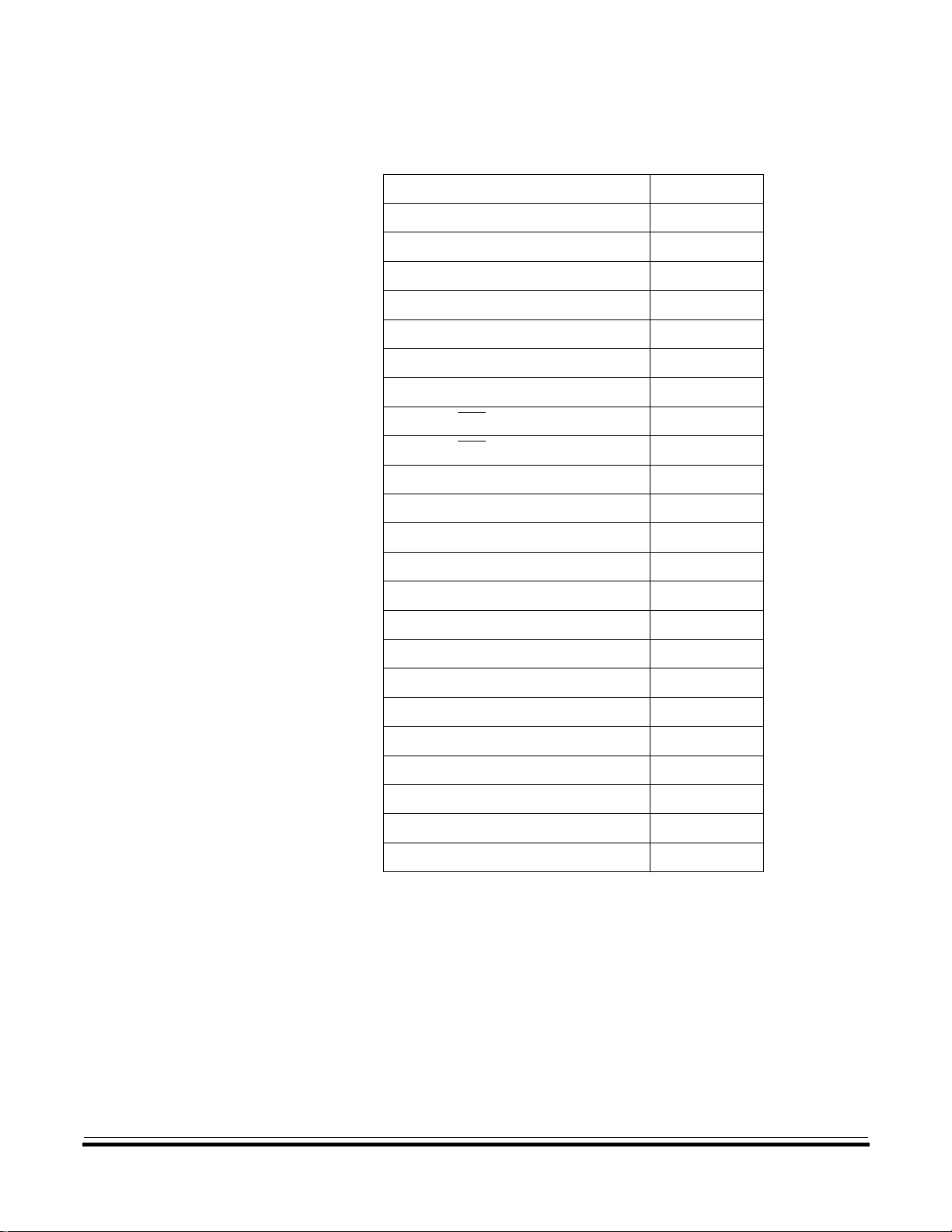
Table 10-3. Jump and Branch Instructions
Instruction Mnemonic
Branch if Carry Bit Clear BCC
Branch if Carry Bit Set BCS
Branch if Equal BEQ
Branch if Half-Carry Bit Clear BHCC
Branch if Half-Carry Bit Set BHCS
Branch if Higher BHI
Branch if Higher or Same BHS
Branch if IRQ Pin High BIH
Branch if IRQ Pin Low BIL
Branch if Lower BLO
Branch if Lower or Same BLS
Instruction Set
Instruction Types
Branch if Interrupt Mask Clear BMC
Branch if Minus BMI
Branch if Interrupt Mask Set BMS
Branch if Not Equal BNE
Branch if Plus BPL
Branch Always BRA
Branch if Bit Clear BRCLR
Branch Never BRN
Branch if Bit Set BRSET
Branch to Subroutine BSR
Unconditional Jump JMP
Jump to Subroutine JSR
MC68HC05RC16 — Rev. 3.0 General Release Specification
MOTOROLA Instruction Set 93
Page 94

Instruction Set
10.4.4 Bit Manipulation Instructions
The CPU can set or clear any writable bit in the first 256 bytes of
memory, which includes I/O registers and on-chip RAM locations. The
CPU can also test and branch based on the state of any bit in any of the
first 256 memory locations.
Table 10-4. Bit Manipulation Instructions
Instruction Mnemonic
Bit Clear BCLR
Branch if Bit Clear BRCLR
Branch if Bit Set BRSET
Bit Set BSET
General Release Specification MC68HC05RC16 — Rev. 3.0
94 Instruction Set MOTOROLA
Page 95

10.4.5 Control Instructions
These instructions act on CPU registers and control CPU operation
during program execution.
Instruction Set
Instruction Types
Table 10-5. Control Instructions
Instruction Mnemonic
Clear Carry Bit CLC
Clear Interrupt Mask CLI
No Operation NOP
Reset Stack Pointer RSP
Return from Interrupt RTI
Return from Subroutine RTS
Set Carry Bit SEC
Set Interrupt Mask SEI
Stop Oscillator and Enable IRQ Pin STOP
Software Interrupt SWI
Transfer Accumulator to Index Register TAX
Transfer Index Register to Accumulator TXA
Stop CPU Clock and Enable Interrupts
WAIT
MC68HC05RC16 — Rev. 3.0 General Release Specification
MOTOROLA Instruction Set 95
Page 96

Instruction Set
10.5 Instruction Set Summary
Table 10-6. Instruction Set Summary
Source
Form
ADC #
ADC
opr
ADC
opr
ADC
opr
ADC
opr
ADC ,X
ADD #
ADD
opr
ADD
opr
ADD
opr
ADD
opr
ADD ,X
AND #
AND
opr
AN
D opr
AND
opr
AND
opr
AND ,X
ASL
opr
ASLA
ASLX
ASL
opr
ASL ,X
ASR
opr
ASRA
ASRX
ASR
opr
ASR ,X
BCC
rel
BCLR
BCS
rel
BEQ
rel
BHCC
BHCS
BHI
rel
BHS
rel
opr
,X
,X
opr
,X
,X
opr
,X
,X
,X
,X
n opr
rel
rel
Add with Carry A ← (A) + (M) + (C) ↕— ↕ ↕ ↕
Add without Carry A ← (A) + (M) ↕— ↕ ↕↕
Logical AND A ← (A) ∧ (M) — — ↕ ↕ —
Arithmetic Shift Left (Same as LSL) — — ↕ ↕↕
Arithmetic Shift Right — — ↕ ↕↕
Branch if Carry Bit Clear PC ← (PC) + 2 +
Clear Bit n Mn ← 0 —————
Branch if Carry Bit Set (Same as BLO) PC ← (PC) + 2 +
Branch if Equal PC ← (PC) + 2 +
Branch if Half-Carry Bit Clear PC ← (PC) + 2 +
Branch if Half-Carry Bit Set PC ← (PC) + 2 +
Branch if Higher PC ← (PC) + 2 +
Branch if Higher or Same PC ← (PC) + 2 +
Operation Description
C
Effect on
CCR
HINZC
0
b7
b7
b0
C
b0
rel
? C = 0 ————— REL 24 rr 3
rel
? C = 1 ————— REL 25 rr 3
rel
? Z = 1 ————— REL 27 rr 3
rel
? H = 0 ————— REL 28 rr 3
rel
? H = 1 ————— REL 29 rr 3
rel
? C ∨ Z = 0 ————— REL 22 rr 3
rel
? C = 0 ————— REL 24 rr 3
Address
IMM
DIR
EXT
IX2
IX1
IX
IMM
DIR
EXT
IX2
IX1
IX
IMM
DIR
EXT
IX2
IX1
IX
DIR
INH
INH
IX1
IX
DIR
INH
INH
IX1
IX
DIR (b0)
DIR (b1)
DIR (b2)
DIR (b3)
DIR (b4)
DIR (b5)
DIR (b6)
DIR (b7)
Mode
A9
B9
C9
D9
E9
F9
AB
BB
CB
DB
EB
FB
A4
B4
C4
D4
E4
F4
38
48
58
68
78
37
47
57
67
77
11
13
15
17
19
1B
1D
1F
Opcode
Operand
ii
dd
hh ll
ee ff
ff
ii
dd
hh ll
ee ff
ff
ii
dd
hh ll
ee ff
ff
dd
ff
dd
ff
dd
dd
dd
dd
dd
dd
dd
dd
Cycles
2
3
4
5
4
3
2
3
4
5
4
3
2
3
4
5
4
3
5
3
3
6
5
5
3
3
6
5
5
5
5
5
5
5
5
5
General Release Specification MC68HC05RC16 — Rev. 3.0
96 Instruction Set MOTOROLA
Page 97

Instruction Set
Instruction Set Summary
Table 10-6. Instruction Set Summary (Continued)
Effect on
Source
Form
BIH
rel
BIL
rel
BIT #
opr
BIT
opr
BIT
opr
BIT
opr
,X
BIT
opr
,X
BIT ,X
BLO
rel
BLS
rel
BMC
rel
BMI
rel
BMS
rel
BNE
rel
BPL
rel
BRA
rel
BRCLR
n opr rel
BRN
rel
BRSET
n opr rel
BSET
n opr
BSR
rel
CLC Clear Carry Bit C ← 0 ———— 0 INH 98 2
CLI Clear Interrupt Mask I ← 0 — 0 — — — INH 9A 2
Branch if IRQ Pin High PC ← (PC) + 2 +
Branch if IRQ Pin Low PC ← (PC) + 2 +
Bit Test Accumulator with Memory Byte (A) ∧ (M) — — ↕ ↕ —
Branch if Lower (Same as BCS) PC ← (PC) + 2 +
Branch if Lower orSame PC ← (PC) + 2 +
Branch if Interrupt Mask Clear PC ← (PC) + 2 +
Branch if Minus PC ← (PC) + 2 +
Branch if Interrupt Mask Set PC ← (PC) + 2 +
Branch if Not Equal PC ← (PC) + 2 +
Branch if Plus PC ← (PC) + 2 +
Branch Always PC ← (PC) + 2 +
Branch if Bit n Clear PC ← (PC) + 2 +
Branch Never PC ← (PC) + 2 +
Branch if Bit n Set PC ← (PC) + 2 +
Set Bit n Mn ← 1 —————
Branch to Subroutine
Operation Description
rel
? IRQ = 1 ————— REL 2F rr 3
rel
? IRQ = 0 ————— REL 2E rr 3
rel
rel
? C ∨ Z = 1 ————— REL 23 rr 3
rel
rel
rel
rel
rel
rel
rel
? Mn = 0 ———— ↕
rel
rel
? Mn = 1 ———— ↕
PC ← (PC) + 2; push (PCL)
SP ← (SP) – 1; push (PCH)
SP ← (SP) – 1
PC ← (PC) +
? C = 1 ————— REL 25 rr 3
? I = 0 ————— REL 2C rr 3
? N = 1 ————— REL 2B rr 3
? I = 1 ————— REL 2D rr 3
? Z = 0 ————— REL 26 rr 3
? N = 0 ————— REL 2A rr 3
? 1 = 1 ————— REL 20 rr 3
? 1 = 0 ————— REL 21 rr 3
rel
CCR
HINZC
————— REL AD rr 6
Address
IMM
DIR
EXT
IX2
IX1
IX
DIR (b0)
DIR (b1)
DIR (b2)
DIR (b3)
DIR (b4)
DIR (b5)
DIR (b6)
DIR (b7)
DIR (b0)
DIR (b1)
DIR (b2)
DIR (b3)
DIR (b4)
DIR (b5)
DIR (b6)
DIR (b7)
DIR (b0)
DIR (b1)
DIR (b2)
DIR (b3)
DIR (b4)
DIR (b5)
DIR (b6)
DIR (b7)
Mode
A5
B5
C5
D5
E5
F5
01
03
05
07
09
0B
0D
0F
00
02
04
06
08
0A
0C
0E
10
12
14
16
18
1A
1C
1E
Opcode
Operand
ii
dd
hh ll
ee ff
ff
dd rr
dd rr
dd rr
dd rr
dd rr
dd rr
dd rr
dd rr
dd rr
dd rr
dd rr
dd rr
dd rr
dd rr
dd rr
dd rr
dd
dd
dd
dd
dd
dd
dd
dd
2
3
4
5
4
3
5
5
5
5
5
5
5
5
5
5
5
5
5
5
5
5
5
5
5
5
5
5
5
5
Cycles
MC68HC05RC16 — Rev. 3.0 General Release Specification
MOTOROLA Instruction Set 97
Page 98

Instruction Set
Source
Form
CLR
opr
CLRA
CLRX
CLR
opr
CLR ,X
CMP #
CMP
opr
CMP
opr
CMP
opr
CMP
opr
CMP ,X
COM
opr
COMA
COMX
COM
opr
COM ,X
CPX #
CPX
opr
CPX
opr
CPX
opr
CPX
opr
CPX ,X
DEC
opr
DECA
DECX
DEC
opr
DEC ,X
EOR #
EOR
opr
EOR
opr
EOR
opr
EOR
opr
EOR ,X
INC
opr
INCA
INCX
INC
opr
INC ,X
JMP
opr
JMP
opr
JMP
opr
JMP
opr
JMP ,X
,X
opr
,X
,X
,X
opr
,X
,X
,X
opr
,X
,X
,X
,X
,X
Clear Byte
Compare Accumulator with Memory Byte (A) – (M) — — ↕ ↕↕
Complement Byte (One’s Complement)
Compare Index Register with Memory Byte (X) – (M) — — ↕↕ ↕
Decrement Byte
EXCLUSIVE OR Accumulator with Memory
Byte
Increment Byte
Unconditional Jump PC ← Jump Address —————
Table 10-6. Instruction Set Summary (Continued)
Effect on
Operation Description
M ← $00
A ← $00
X ← $00
M ← $00
M ← $00
M ← (M) = $FF – (M)
A ← (A) = $FF – (A)
X ← (X) = $FF – (X)
M ← (M) = $FF – (M)
M ← (M) = $FF – (M)
M ← (M) – 1
A ← (A) – 1
X ← (X) – 1
M ← (M) – 1
M ← (M) – 1
A ← (A) ⊕ (M) — — ↕ ↕ —
M ← (M) + 1
A ← (A) + 1
X ← (X) + 1
M ← (M) + 1
M ← (M) + 1
CCR
HINZC
—— 0 1—
—— ↕ ↕
—— ↕ ↕—
—— ↕ ↕—
1
Mode
Address
DIR
INH
INH
IX1
IX
IMM
DIR
EXT
IX2
IX1
IX
DIR
INH
INH
IX1
IX
IMM
DIR
EXT
IX2
IX1
IX
DIR
INH
INH
IX1
IX
IMM
DIR
EXT
IX2
IX1
IX
DIR
INH
INH
IX1
IX
DIR
EXT
IX2
IX1
IX
Opcode
dd
3F
4F
5F
6F
7F
A1
dd
B1
hh ll
C1
ee ff
D1
E1
F1
dd
33
43
53
63
73
A3
dd
B3
hh ll
C3
ee ff
D3
E3
F3
dd
3A
4A
5A
6A
7A
A8
dd
B8
hh ll
C8
ee ff
D8
E8
F8
dd
3C
4C
5C
6C
7C
dd
BC
hh ll
CC
ee ff
DC
EC
FC
Cycles
Operand
5
3
3
6
ff
5
ii
2
3
4
5
ff
4
3
5
3
3
6
ff
5
ii
2
3
4
5
ff
4
3
5
3
3
6
ff
5
ii
2
3
4
5
ff
4
3
5
3
3
6
ff
5
2
3
4
ff
3
2
General Release Specification MC68HC05RC16 — Rev. 3.0
98 Instruction Set MOTOROLA
Page 99

Source
Form
JSR
opr
JSR
opr
JSR
opr
JSR
opr
JSR ,X
LDA #
LDA
opr
LDA
opr
LDA
opr
LDA
opr
LDA ,X
LDX #
LDX
opr
LDX
opr
LDX
opr
LDX
opr
LDX ,X
LSL
opr
LSLA
LSLX
LSL
opr
LSL ,X
LSR
opr
LSRA
LSRX
LSR
opr
LSR ,X
opr
opr
Instruction Set
Instruction Set Summary
Table 10-6. Instruction Set Summary (Continued)
Effect on
Operation Description
PC ← (PC) + n (n = 1, 2, or 3)
,X
,X
,X
,X
,X
,X
,X
,X
Jump to Subroutine
Load Accumulator with Memory Byte A ← (M) — — ↕ ↕ —
Load Index Register with Memory Byte X ← (M) — — ↕ ↕—
Logical Shift Left (Same as ASL) — — ↕ ↕↕
Logical Shift Right — — 0 ↕↕
Push (PCL); SP ← (SP) – 1
Push (PCH); SP ← (SP) – 1
PC ← Effective Address
C
b7
b7
0
b0
C0
b0
CCR
HINZC
—————
Mode
Address
DIR
EXT
IX2
IX1
IX
IMM
DIR
EXT
IX2
IX1
IX
IMM
DIR
EXT
IX2
IX1
IX
DIR
INH
INH
IX1
IX
DIR
INH
INH
IX1
IX
Opcode
dd
BD
hh ll
CD
ee ff
DD
ED
FD
A6
dd
B6
hh ll
C6
ee ff
D6
E6
F6
AE
dd
BE
hh ll
CE
ee ff
DE
EE
FE
dd
38
48
58
68
78
dd
34
44
54
64
74
Cycles
Operand
5
6
7
ff
6
5
ii
2
3
4
5
ff
4
3
ii
2
3
4
5
ff
4
3
5
3
3
6
ff
5
5
3
3
6
ff
5
MUL Unsigned Multiply X : A← (X) × (A) 0 — — — 0 INH 42 11
NEG
opr
NEGA
NEGX
NEG
opr
,X
NEG ,X
NOP No Operation ————— INH 9D 2
ORA #
opr
ORA
opr
ORA
opr
ORA
opr
,X
ORA
opr
,X
ORA ,X
ROL
opr
ROLA
ROLX
ROL
opr
,X
ROL ,X
Negate Byte (Two’s Complement)
Logical OR Accumulator with Memory A ← (A) ∨ (M) — — ↕ ↕ —
Rotate Byte Left through Carry Bit — — ↕ ↕↕
M ← –(M) = $00 – (M)
A ← –(A) = $00 – (A)
X ← –(X) = $00 – (X)
M ← –(M) = $00 – (M)
M ← –(M) = $00 – (M)
C
b7
b0
—— ↕ ↕↕
DIR
INH
INH
IX1
IX
IMM
DIR
EXT
IX2
IX1
IX
DIR
INH
INH
IX1
IX
30
40
50
60
70
AA
BA
CA
DA
EA
FA
39
49
59
69
79
dd
ff
ii
dd
hh ll
ee ff
ff
dd
ff
5
3
3
6
5
2
3
4
5
4
3
5
3
3
6
5
MC68HC05RC16 — Rev. 3.0 General Release Specification
MOTOROLA Instruction Set 99
Page 100
Instruction Set
Table 10-6. Instruction Set Summary (Continued)
Effect on
Source
Form
ROR
opr
RORA
RORX
ROR
opr
,X
ROR ,X
RSP Reset Stack Pointer SP ← $00FF ————— INH 9C 2
RTI Return from Interrupt
RTS Return from Subroutine
SBC #
opr
SBC
opr
SBC
opr
SBC
opr
,X
SBC
opr
,X
SBC ,X
SEC Set Carry Bit C ← 1 ———— 1 INH 99 2
SEI Set Interrupt Mask I ← 1 — 1 — — — INH 9B 2
STA
opr
STA
opr
STA
opr
,X
STA
opr
,X
STA ,X
STOP Stop Oscillator and Enable IRQ Pin — 0 — — — INH 8E 2
STX
opr
STX
opr
STX
opr
,X
STX
opr
,X
STX ,X
SUB #
opr
SUB
opr
SUB
opr
SUB
opr
,X
SUB
opr
,X
SUB ,X
SWI Software Interrupt
TAX Transfer Accumulator to Index Register X ← (A) ————— INH 97 2
Rotate Byte Right through Carry Bit — — ↕ ↕↕
Subtract Memory Byte and Carry Bit from
Accumulator
Store Accumulator in Memory M ← (A) — — ↕ ↕ —
Store Index Register In Memory M ← (X) — — ↕ ↕ —
Subtract Memory Byte from Accumulator A ← (A) – (M) — — ↕↕↕
Operation Description
b7
SP ← (SP) + 1; Pull (CCR)
SP ← (SP) + 1; Pull (A)
SP ← (SP) + 1; Pull (X)
SP ← (SP) + 1; Pull (PCH)
SP ← (SP) + 1; Pull (PCL)
SP ← (SP) + 1; Pull (PCH)
SP ← (SP) + 1; Pull (PCL)
A ← (A) – (M) – (C) — — ↕↕↕
PC ← (PC) + 1; Push (PCL)
SP ← (SP) – 1; Push (PCH)
SP ← (SP) – 1; Push (X)
SP ← (SP) – 1; Push (A)
SP ← (SP) – 1; Push (CCR)
SP ← (SP) – 1; I ← 1
PCH ← Interrupt Vector High Byte
PCL ← Interrupt Vector Low Byte
b0
C
CCR
HINZC
↕ ↕↕↕↕ INH 80 9
————— INH 81 6
— 1 — — — INH 83 10
Mode
Address
DIR
INH
INH
IX1
IX
IMM
DIR
EXT
IX2
IX1
IX
DIR
EXT
IX2
IX1
IX
DIR
EXT
IX2
IX1
IX
IMM
DIR
EXT
IX2
IX1
IX
Opcode
dd
36
46
56
66
76
A2
dd
B2
hh ll
C2
ee ff
D2
E2
F2
dd
B7
hh ll
C7
ee ff
D7
E7
F7
dd
BF
hh ll
CF
ee ff
DF
EF
FF
A0
dd
B0
hh ll
C0
ee ff
D0
E0
F0
Operand
ff
ii
ff
ff
ff
ii
ff
Cycles
5
3
3
6
5
2
3
4
5
4
3
4
5
6
5
4
4
5
6
5
4
2
3
4
5
4
3
General Release Specification MC68HC05RC16 — Rev. 3.0
100 Instruction Set MOTOROLA
 Loading...