

Page 1

查询M68300供应商
MOTOROLA
MC68360
QUad Integrated
Communications Controller
User’s Manual
Motorola reserves the right to make changes without further notice to any products herein to improve reliability, function or design. Motorola does not assume any
liability arising out of the application or use of any product or circuit described herein; neither does it convey any license under its patent rights nor the rights of
others. Motorola products are not designed, intended, or authorized for use as components in systems intended for surgical implant into the body, or other
applications intended to support or sustain life, or for any other application in which the failure of the Motorola product could create a situation where personal
injury or death may occur. Should Buyer purchase or use Motorola products for any such unintended or unauthorized application, Buyer shall indemnify and hold
Motorola and its officers, employees, subsidiaries, affiliates, and distributors harmless against all claims, costs, damages, and expenses, and reasonable attorney
fees arising out of, directly or indirectly, any claim of personal injury or death associated with such unintended or unauthorized use, even if such claim alleges that
Motorola was negligent regarding the design or manufacture of the part. Motorola and the are registered trademarks of Motorola, Inc. Motorola, Inc. is an
Equal Opportunity/Affirmative Action Employer.
Page 2

ii MC68360 USER’S MANUAL MOTOROLA
Page 3

PREFACE
The complete documentation package for the MC68360 consists of the MC68360UM/AD,
MC68360 QUad Integrated Communications Controller User’s Manual
MC68000 Family Programmer’s Reference Manual,
Integrated Communications Controller Product Brief
and the MC68360/D,
.
, M68000PM/AD,
MC68360 QUad
MC68360 QUad Integrated Communications Controller User’s Manual
The
programming, capabilities, registers, and operation of the MC68360 and the MC68EN360;
MC68000 Family Programmer’s Reference Manual
the
the
MC68360; and
provides a brief description of the MC68360 capabilities.
This user’s manual is organized as follows:
Section 1 Introduction
Section 2 Signal Descriptions
Section 3 Memory Map
Section 4 Bus Operation
Section 5 CPU32+
Section 6 System Integration Module (SIM60)
Section 7 Communication Processor Module (CPM)
Section 8 IEEE 1149.1 Test Access Port
Section 9 Applications
Section 10 Electrical Characteristics
Section 11 Ordering Information and Mechanical Data
Appendix A Serial Performance
Appendix B Development Tools and Support
Appendix C RISC Microcode from RAM
Appendix D MC68MH360 Product Brief
MC68360 QUad Integrated Communications Controller Product Brief
provides instruction details for the
describes the
MOTOROLA MC68360 USER’S MANUAL iii
Page 4

iv MC68360 USER’S MANUAL MOTOROLA
Page 5

Table of Contents
Paragraph Title Page
Number Number
Section 1
Introduction
1.1 QUICC Key Features .............................................................................. 1-1
1.2 QUICC Architecture Overview................................................................. 1-4
1.2.1 CPU32+ Core.......................................................................................... 1-5
1.2.2 System Integration Module (SIM60)........................................................1-5
1.2.3 Communications Processor Module (CPM)............................................1-6
1.3 Upgrading Designs from the MC68302................................................... 1-6
1.3.1 Architectural Approach............................................................................ 1-6
1.3.2 Hardware Compatibility Issues................................................................1-7
1.3.3 Software Compatibility Issues................................................................. 1-7
1.4 QUICC Glueless System Design............................................................. 1-8
1.5 QUICC Serial Configurations .................................................................. 1-9
1.6 QUICC Serial Configuration Examples ................................................. 1-16
1.7 QUICC System Bus Configurations ...................................................... 1-17
Section 2
Signal Descriptions
2.1 System Bus Signal Index ........................................................................2-1
2.1.1 Address Bus............................................................................................ 2-1
2.1.1.1 Address Bus (A27–A0)............................................................................2-1
2.1.1.2 Address Bus (A31–A28)..........................................................................2-1
2.1.2 Function Codes (FC3–FC0).................................................................... 2-5
2.1.3 Data Bus.................................................................................................. 2-5
2.1.3.1 Data Bus (D31–D16)............................................................................... 2-5
2.1.3.2 Data Bus (D15–D0)................................................................................. 2-6
2.1.4 Parity....................................................................................................... 2-6
2.1.4.1 Parity (PRTY0)........................................................................................ 2-6
2.1.4.2 Parity (PRTY1)........................................................................................ 2-6
2.1.4.3 Parity (PRTY2)........................................................................................ 2-6
2.1.4.4 Parity (PRTY3)........................................................................................ 2-6
2.1.5 Memory Controller...................................................................................2-6
2.1.5.1 Chip Select/Row Address Select (CS6–CS0/RAS6–RAS0) ...................2-6
2.1.5.2 Chip Select/Row Address Select/Interrupt Acknowledge (CS7/RAS7/IACK7).
2-6
2.1.5.3 Column Address Select/Interrupt Acknowledge (CAS3–CAS0/IACK6, 3, 2,
1). 2-7
2.1.5.4 Address Multiplex (AMUX)...................................................................... 2-7
2.1.6 Interrupt Request Level (IRQ7–IRQ1).....................................................2-7
2.1.7 Bus Control Signals.................................................................................2-7
2.1.7.1 Data and Size Acknowledge (DSACK1–DSACK0)................................. 2-8
2.1.7.2 Autovector/Interrupt Acknowledge (AVEC/IACK5)..................................2-8
2.1.7.3 Address Strobe (AS). ..............................................................................2-8
2.1.7.4 Data Strobe (DS).....................................................................................2-8
MOTOROLA
MC68360 USER’S MANUAL
i
Page 6

ii
Table of Contents
Paragraph Title Page
Number Number
2.1.7.5 Transfer Size (SIZ1, SIZ0).......................................................................2-8
2.1.7.6 Read/Write (R/W).....................................................................................2-8
2.1.7.7 Output Enable/Address Multiplex (OE/AMUX).........................................2-9
2.1.7.8 Byte Write Enable (WE3–WE0)...............................................................2-9
2.1.8 Bus Arbitration Signals.............................................................................2-9
2.1.8.1 Bus Request (BR)....................................................................................2-9
2.1.8.2 Bus Grant (BG)........................................................................................2-9
2.1.8.3 Bus Grant Acknowledge (BGACK). .........................................................2-9
2.1.8.4 Read-Modify-Write Cycle/Initial Configuration (RMC/CONFIG0).............2-9
2.1.8.5 Bus Clear Out/Initial Configuration/Row Address Select Double-Drive (BCLRO/CONFIG1/RAS2DD).2-9
2.1.9 System Control Signals..........................................................................2-10
2.1.9.1 Soft Reset (RESETS). ...........................................................................2-10
2.1.9.2 Hard Reset (RESETH)...........................................................................2-10
2.1.9.3 Halt (HALT)............................................................................................2-10
2.1.9.4 Bus Error (BERR). .................................................................................2-10
2.1.10 Clock Signals.........................................................................................2-10
2.1.10.1 System Clock Outputs (CLKO2–CLKO1). .............................................2-10
2.1.10.2 Crystal Oscillator (EXTAL, XTAL)..........................................................2-11
2.1.10.3 External Filter Capacitor (XFC)..............................................................2-11
2.1.10.4 Clock Mode Select (MODCK1–MODCK0).............................................2-11
2.1.11 Instrumentation and Emulation Signals .................................................2-11
2.1.11.1 Instruction Fetch/Development Serial Input (IFETCH/DSI)....................2-11
2.1.11.2 Instruction Pipe/Development Serial Output (
2.1.11.3 Instruction Pipe/Row Address Select Double-Drive (
IPIPE0/DSO )...................2-11
IPIPE1/RAS1DD ).2-11
2.1.11.4 Breakpoint/Development Serial clock (BKPT/DSCLK). .........................2-11
2.1.11.5 Freeze/Initial Configuration (FREEZE/CONFIG2). ................................2-12
2.1.12 Test Signals...........................................................................................2-12
2.1.12.1 TRI-State Signal (TRIS).........................................................................2-12
2.1.12.2 Test Reset (TRST).................................................................................2-12
2.1.12.3 Test Clock (TCK). ..................................................................................2-12
2.1.12.4 Test Mode Select (TMS)........................................................................2-12
2.1.12.5 Test Data In (TDI)..................................................................................2-12
2.1.12.6 Test Data Out (TDO)..............................................................................2-12
2.1.13 Initial Configuration Pins (CONFIG).......................................................2-12
2.1.14 Power Signals........................................................................................2-13
2.1.14.1 VCCSYN and GNDSYN.........................................................................2-13
2.1.14.2 VCCCLK and GNDCLK. ........................................................................2-13
2.1.14.3 GNDS1 and GNDS2..............................................................................2-13
2.1.14.4 VCC and GND. ......................................................................................2-13
2.1.14.5 NC4–NC1...............................................................................................2-13
2.2 System Bus Signal Index in Slave Mode...............................................2-14
2.3 On-Chip Peripherals Signal Index..........................................................2-15
Section 3
MC68360 USER’S MANUAL
MOTOROLA
Page 7

Table of Contents
Paragraph Title Page
Number Number
QUICC Memory Map
3.1 Dual-Port RAM Memory Map.................................................................. 3-2
3.2 CPM Sub-Module Base Addresses.........................................................3-3
3.3 Internal Registers Memory Map.............................................................. 3-4
3.3.1 SIM Registers Memory Map....................................................................3-4
3.3.2 CPM Registers Memory Map.................................................................. 3-6
Section 4
Bus Operation
4.1 Bus Transfer Signals............................................................................... 4-2
4.1.1 Bus Control Signals.................................................................................4-3
4.1.2 Function Codes (FC3–FC0).................................................................... 4-3
4.1.3 Address Bus (A31–A0)............................................................................4-4
4.1.4 Address Strobe (AS) ...............................................................................4-4
4.1.5 Data Bus (D31-D0)..................................................................................4-4
4.1.6 Data Strobe (DS).....................................................................................4-4
4.1.7 Output Enable (OE).................................................................................4-4
4.1.8 Byte Write Enable (WE0, WE1, WE2, WE3)........................................... 4-4
4.1.9 Bus Cycle Termination Signals ............................................................... 4-5
4.1.9.1 Data transfer and size acknowledge (DSACK1 and DSACK0)............... 4-5
4.1.9.2 Bus Error (BERR)....................................................................................4-5
4.1.9.3 Autovector (AVEC).................................................................................. 4-6
4.2 Data Transfer Mechanism....................................................................... 4-6
4.2.1 Dynamic Bus Sizing ................................................................................4-6
4.2.2 Misaligned Operands ............................................................................4-11
4.2.3 Effects of Dynamic Bus Sizing and Operand Misalignment.................. 4-19
4.2.4 Bus Operation .......................................................................................4-20
4.2.5 Synchronous Operation with DSACKx.................................................. 4-21
4.2.6 Fast Termination Cycles........................................................................ 4-21
4.3 Data Transfer Cycles............................................................................. 4-22
4.3.1 Read Cycle............................................................................................4-23
4.3.2 Write Cycle............................................................................................ 4-26
4.3.3 Read-Modify-Write Cycle ...................................................................... 4-28
4.4 CPU Space Cycles................................................................................4-31
4.4.1 Breakpoint Acknowledge Cycle.............................................................4-31
4.4.2 LPSTOP Broadcast Cycle..................................................................... 4-35
4.4.3 Module Base Address Register (MBAR) Access .................................. 4-36
4.4.4 Interrupt Acknowledge Bus Cycles........................................................ 4-36
4.4.4.1 Interrupt Acknowledge Cycle—Terminated Normally............................ 4-36
4.4.4.2 Autovector Interrupt Acknowledge Cycle. .............................................4-38
4.4.4.3 Spurious Interrupt Cycle........................................................................4-40
4.5 Bus Exception Control Cycles............................................................... 4-41
4.5.1 Bus Errors ............................................................................................. 4-42
4.5.2 Retry Operation..................................................................................... 4-44
4.5.3 Halt Operation....................................................................................... 4-46
4.5.4 Double Bus Fault...................................................................................4-48
MOTOROLA
MC68360 USER’S MANUAL
iii
Page 8

iv
Table of Contents
Paragraph Title Page
Number Number
4.6 Bus Arbitration .......................................................................................4-49
4.6.1 Bus Request ..........................................................................................4-52
4.6.2 Bus Grant...............................................................................................4-53
4.6.3 Bus Grant Acknowledge ........................................................................4-53
4.6.4 Bus Arbitration Control...........................................................................4-54
4.6.5 Slave (Disable CPU32+) Mode Bus Arbitration .....................................4-55
4.6.6 Slave (Disable CPU32+) Mode Bus Exceptions....................................4-59
4.6.6.1 HALT......................................................................................................4-59
4.6.6.2 RETRY...................................................................................................4-59
4.6.7 Internal Accesses...................................................................................4-59
4.6.8 Show Cycles..........................................................................................4-62
4.7 Reset Operation.....................................................................................4-63
Section 5
CPU32+
5.1 Overview..................................................................................................5-1
5.1.1 Features...................................................................................................5-2
5.1.2 Loop Mode Instruction Execution.............................................................5-3
5.1.3 Vector Base Register...............................................................................5-4
5.1.4 Exception Handling..................................................................................5-4
5.1.5 Addressing Modes...................................................................................5-5
5.2 Architecture Summary .............................................................................5-5
5.2.1 Programming Model.................................................................................5-6
5.2.2 Registers..................................................................................................5-7
5.3 Instruction Set..........................................................................................5-8
5.3.1 M68000 Family Compatibility.................................................................5-10
5.3.1.1 New Instructions. ...................................................................................5-10
5.3.1.2 Low-Power Stop (LPSTOP)...................................................................5-10
5.3.1.3 Table Lookup and Interpolate (TBL)......................................................5-10
5.3.1.4 Unimplemented Instructions. .................................................................5-10
5.3.2 Instruction Format and Notation.............................................................5-10
5.3.3 Instruction Summary..............................................................................5-13
5.3.3.1 Condition Code Register........................................................................5-17
5.3.3.2 Data Movement Instructions..................................................................5-19
5.3.3.3 Integer Arithmetic Operations................................................................5-19
5.3.3.4 Logic Instructions...................................................................................5-21
5.3.3.5 Shift and Rotate Instructions..................................................................5-22
5.3.3.6 Bit Manipulation Instructions..................................................................5-23
5.3.3.7 Binary-Coded Decimal (BCD) Instructions.............................................5-24
5.3.3.8 Program Control Instructions.................................................................5-24
5.3.3.9 System Control Instructions...................................................................5-25
5.3.3.10 Condition Tests......................................................................................5-26
5.3.4 Using the TBL Instructions.....................................................................5-27
5.3.4.1 Table Example 1: Standard Usage........................................................5-28
5.3.4.2 Table Example 2: Compressed Table....................................................5-29
MC68360 USER’S MANUAL
MOTOROLA
Page 9

Table of Contents
Paragraph Title Page
Number Number
5.3.4.3 Table Example 3: 8-Bit Independent Variable.......................................5-30
5.3.4.4 Table Example 4: Maintaining Precision............................................... 5-32
5.3.4.5 Table Example 5: Surface Interpolations ..............................................5-33
5.3.5 Nested Subroutine Calls........................................................................ 5-33
5.3.6 Pipeline Synchronization with the NOP Instruction............................... 5-34
5.4 Processing States .................................................................................5-34
5.4.1 State Transitions ...................................................................................5-34
5.4.2 Privilege Levels..................................................................................... 5-34
5.4.2.1 Supervisor Privilege Level.....................................................................5-35
5.4.2.2 User Privilege Level .............................................................................. 5-35
5.4.2.3 Changing Privilege Level....................................................................... 5-35
5.5 Exception Processing............................................................................5-36
5.5.1 Exception Vectors .................................................................................5-36
5.5.1.1 Types of Exceptions.............................................................................. 5-36
5.5.1.2 Exception Processing Sequence........................................................... 5-38
5.5.1.3 Exception Stack Frame......................................................................... 5-38
5.5.1.4 Multiple Exceptions ...............................................................................5-39
5.5.2 Processing of Specific Exceptions ........................................................5-40
5.5.2.1 Reset..................................................................................................... 5-40
5.5.2.2 Bus Error............................................................................................... 5-40
5.5.2.3 Address Error........................................................................................ 5-42
5.5.2.4 Instruction Traps.................................................................................... 5-42
5.5.2.5 Software Breakpoints............................................................................ 5-43
5.5.2.6 Hardware Breakpoints...........................................................................5-43
5.5.2.7 Format Error.......................................................................................... 5-43
5.5.2.8 Illegal or Unimplemented Instructions................................................... 5-44
5.5.2.9 Privilege Violations................................................................................ 5-44
5.5.2.10 Tracing ..................................................................................................5-45
5.5.2.11 Interrupts............................................................................................... 5-46
5.5.2.12 Return from Exception........................................................................... 5-47
5.5.3 Fault Recovery...................................................................................... 5-48
5.5.3.1 Types of Faults......................................................................................5-51
5.5.3.1.1 Type I—Released Write Faults ............................................................. 5-51
5.5.3.1.2 Type II—Prefetch, Operand, RMW, and MOVEP Faults....................... 5-51
5.5.3.1.3 Type III—Faults During MOVEM Operand Transfer ............................. 5-52
5.5.3.1.4 Type IV—Faults During Exception Processing .....................................5-52
5.5.3.2 Correcting a Fault..................................................................................5-53
5.5.3.2.1 Type I—Completing Released Writes via Software .............................. 5-53
5.5.3.2.2 Type I—Completing Released Writes via RTE ..................................... 5-53
5.5.3.2.3 Type II—Correcting Faults via RTE....................................................... 5-54
5.5.3.2.4 Type III—Correcting Faults via Software............................................... 5-54
5.5.3.2.5 Type III—Correcting Faults by Conversion and Restart........................5-55
5.5.3.2.6 Type III—Correcting Faults via RTE...................................................... 5-55
5.5.3.2.7 Type IV—Correcting Faults via Software.............................................. 5-55
5.5.4 CPU32+ Stack Frames ......................................................................... 5-56
MOTOROLA
MC68360 USER’S MANUAL
v
Page 10

vi
Table of Contents
Paragraph Title Page
Number Number
5.5.4.1 Four-Word Stack Frame ........................................................................5-56
5.5.4.2 Six-Word Stack Frame...........................................................................5-56
5.5.4.3 Bus Error Stack Frame ..........................................................................5-56
5.6 Development Support............................................................................5-59
5.6.1 CPU32+ Integrated Development Support ............................................5-59
5.6.1.1 Background Debug Mode (BDM) Overview...........................................5-59
5.6.1.2 Deterministic Opcode Tracking Overview..............................................5-60
5.6.1.3 On-Chip Hardware Breakpoint Overview...............................................5-60
5.6.2 Background Debug Mode......................................................................5-60
5.6.2.1 Enabling BDM........................................................................................5-60
5.6.2.2 BDM Sources.........................................................................................5-61
5.6.2.2.1 External BKPT Signal ............................................................................5-62
5.6.2.2.2 BGND Instruction...................................................................................5-62
5.6.2.2.3 Double Bus Fault ...................................................................................5-62
5.6.2.3 Entering BDM.........................................................................................5-62
5.6.2.4 Command Execution..............................................................................5-62
5.6.2.5 BDM Registers.......................................................................................5-63
5.6.2.5.1 Fault Address Register (FAR)................................................................5-63
5.6.2.5.2 Return Program Counter (RPC).............................................................5-63
5.6.2.5.3 Current Instruction Program Counter (PCC)..........................................5-63
5.6.2.6 Returning from BDM..............................................................................5-63
5.6.2.7 Serial Interface.......................................................................................5-63
5.6.2.7.1 CPU Serial Logic....................................................................................5-65
5.6.2.7.2 Development System Serial Logic.........................................................5-66
5.6.2.8 Command Set........................................................................................5-68
5.6.2.8.1 Command Format..................................................................................5-68
5.6.2.8.2 Command Sequence Diagram...............................................................5-69
5.6.2.8.3 Command Set Summary........................................................................5-69
5.6.2.8.4 Read A/D Register (RAREG/RDREG)...................................................5-71
5.6.2.8.5 Write A/D Register (WAREG/WDREG) .................................................5-71
5.6.2.8.6 Read System Register (RSREG)...........................................................5-71
5.6.2.8.7 Write System Register (WSREG)..........................................................5-72
5.6.2.8.8 Read Memory Location (READ) ............................................................5-73
5.6.2.8.9 Write Memory Location (WRITE)...........................................................5-74
5.6.2.8.10 Dump Memory Block (DUMP)................................................................5-75
5.6.2.8.11 Fill Memory Block (FILL)........................................................................5-76
5.6.2.8.12 Resume Execution (GO)........................................................................5-77
5.6.2.8.13 Call User Code (CALL)..........................................................................5-77
5.6.2.8.14 Reset Peripherals (RST)........................................................................5-79
5.6.2.8.15 No Operation (NOP) ..............................................................................5-79
5.6.2.8.16 Future Commands.................................................................................5-80
5.6.3 Deterministic Opcode Tracking..............................................................5-80
5.6.3.1 Instruction Fetch (IFETCH)....................................................................5-80
5.6.3.2 Instruction Pipe (IPIPE1–IPIPE0) ..........................................................5-80
5.6.3.3 Opcode Tracking during Loop Mode......................................................5-82
MC68360 USER’S MANUAL
MOTOROLA
Page 11

Table of Contents
Paragraph Title Page
Number Number
5.7 Instruction Execution Timing................................................................. 5-82
5.7.1 Resource Scheduling............................................................................ 5-83
5.7.1.1 Microsequencer.....................................................................................5-83
5.7.1.2 Instruction Pipeline................................................................................ 5-83
5.7.1.3 Bus Controller Resources ..................................................................... 5-83
5.7.1.3.1 Prefetch Controller ................................................................................ 5-84
5.7.1.3.2 Write-Pending Buffer............................................................................. 5-84
5.7.1.3.3 Microbus Controller............................................................................... 5-85
5.7.1.4 Instruction Execution Overlap ...............................................................5-85
5.7.1.5 Effects of Wait States............................................................................ 5-86
5.7.1.6 Instruction Execution Time Calculation................................................. 5-86
5.7.1.7 Effects of Negative Tails........................................................................ 5-87
5.7.2 Instruction Timing Tables...................................................................... 5-88
5.7.2.1 Fetch Effective Address ........................................................................5-90
5.7.2.2 Calculate Effective Address ..................................................................5-91
5.7.2.3 MOVE Instruction.................................................................................. 5-92
5.7.2.4 Special-Purpose MOVE Instruction.......................................................5-92
5.7.2.5 Arithmetic/Logic Instructions ................................................................. 5-93
5.7.2.6 Immediate Arithmetic/Logic Instructions................................................ 5-95
5.7.2.7 Binary-Coded Decimal and Extended Instructions................................5-95
5.7.2.8 Single Operand Instructions.................................................................. 5-96
5.7.2.9 Shift/Rotate Instructions........................................................................ 5-96
5.7.2.10 Bit Manipulation Instructions .................................................................5-97
5.7.2.11 Conditional Branch Instructions............................................................. 5-98
5.7.2.12 Control Instructions ...............................................................................5-99
5.7.2.13 Exception-Related Instructions and Operations.................................. 5-100
5.7.2.14 Save and Restore Operations............................................................. 5-101
Section 6
System Integration Module (SIM60)
6.1 Module Overview..................................................................................... 6-1
6.2 Module Base Address Register (MBAR)................................................. 6-3
6.3 System Configuration and Protection......................................................6-3
6.3.1 System Configuration.............................................................................. 6-5
6.3.1.1 SIM60 Interrupt Generation.....................................................................6-6
6.3.1.2 Simultaneous SIM60 Interrupt Sources................................................... 6-8
6.3.1.2.1 Bus Monitor............................................................................................. 6-8
6.3.1.2.2 Spurious Interrupt Monitor.......................................................................6-8
6.3.1.2.3 Double Bus Fault Monitor........................................................................6-9
6.3.1.2.4 Software Watchdog Timer (SWT) ........................................................... 6-9
6.3.2 Periodic Interrupt Timer (PIT)................................................................6-10
6.3.2.1 PIT Period Calculation........................................................................... 6-10
6.3.2.2 Using the PIT as a Real-Time Clock..................................................... 6-11
6.3.3 Freeze Support...................................................................................... 6-11
6.3.4 Low-Power Stop Support ......................................................................6-11
6.4 Low Power in Normal Operation ........................................................... 6-12
MOTOROLA
MC68360 USER’S MANUAL
vii
Page 12

Table of Contents
Paragraph Title Page
Number Number
6.5 SIM60 System Clock Generation...........................................................6-12
6.5.1 Clock Generation Methods ....................................................................6-12
6.5.2 Oscillator Prescaler (Divide by 128).......................................................6-13
6.5.3 Phase-Locked Loop (PLL).....................................................................6-14
6.5.3.1 Frequency Multiplication........................................................................6-14
6.5.3.2 Skew Elimination....................................................................................6-15
6.5.4 Low-Power Divider.................................................................................6-15
6.5.5 QUICC Internal Clock Signals................................................................6-15
6.5.5.1 SPCLK...................................................................................................6-16
6.5.5.2 General System Clock...........................................................................6-16
6.5.5.3 BRGCLK................................................................................................6-17
6.5.5.4 SyncCLK................................................................................................6-17
6.5.5.5 SIMCLK..................................................................................................6-18
6.5.5.6 CLKO1...................................................................................................6-18
6.5.5.7 CLKO2...................................................................................................6-18
6.5.6 PLL Power Pins .....................................................................................6-19
6.5.6.1 VCCSYN................................................................................................6-19
6.5.6.2 GNDSYN................................................................................................6-19
6.5.6.3 XFC........................................................................................................6-19
6.5.7 CLKO Power Pins..................................................................................6-19
6.5.7.1 VCCCLK ................................................................................................6-19
6.5.7.2 GNDCLK................................................................................................6-19
6.5.8 Configuration Pins (MODCK1–MODCK0) .............................................6-19
6.6 Breakpoint Logic....................................................................................6-20
6.7 External Bus Interface Control...............................................................6-21
6.7.1 Initial Configuration................................................................................6-22
6.7.2 Port D.....................................................................................................6-22
6.7.3 Port E.....................................................................................................6-23
6.8 Slave (Disable CPU32+) Mode..............................................................6-23
6.8.1 MBAR in a Multiple QUICC System.......................................................6-24
6.8.2 Global Chip Select (CS0) in Slave Mode...............................................6-25
6.8.3 Bus Clear in Slave Mode .......................................................................6-25
6.8.4 Interrupts in Slave Mode........................................................................6-26
6.8.5 Pin Differences in Slave Mode...............................................................6-26
6.8.6 Other Functionality in Slave Mode.........................................................6-27
6.9 Programmer’s Model..............................................................................6-27
6.9.1 Module Base Address Register (MBAR)................................................6-27
6.9.2 Module Base Address Register Enable (MBARE).................................6-29
6.9.3 System Configuration and Protection Registers....................................6-29
6.9.3.1 Module Configuration Register (MCR)...................................................6-29
6.9.3.2 Autovector Register (AVR).....................................................................6-34
6.9.3.3 Reset Status Register (RSR).................................................................6-34
6.9.3.4 Software Watchdog Interrupt Vector Register (SWIV)...........................6-35
6.9.3.5 System Protection Control Register (SYPCR).......................................6-35
6.9.3.6 Periodic Interrupt Control Register (PICR).............................................6-37
viii
MC68360 USER’S MANUAL
MOTOROLA
Page 13

Table of Contents
Paragraph Title Page
Number Number
6.9.3.7 Periodic Interrupt Timer Register (PITR)...............................................6-38
6.9.3.8 Software Service Register (SWSR)....................................................... 6-39
6.9.3.9 CLKO Control Register (CLKOCR)....................................................... 6-39
6.9.3.10 PLL Control Register (PLLCR).............................................................. 6-40
6.9.3.11 Clock Divider Control Register (CDVCR).............................................. 6-42
6.9.3.12 Breakpoint Address Register (BKAR) ................................................... 6-44
6.9.3.13 Breakpoint Control Register (BKCR).....................................................6-44
6.9.4 Port E Pin Assignment Register (PEPAR) ............................................ 6-48
6.10 Memory Controller.................................................................................6-50
6.10.1 Memory Controller Key Features .......................................................... 6-50
6.10.2 Memory Controller Overview.................................................................6-51
6.11 General-Purpose Chip-Select Overview (SRAM Banks)....................... 6-56
6.11.1 Associated Registers............................................................................. 6-56
6.11.2 8-, 16-, and 32-Bit Port Size Configuration............................................ 6-56
6.11.3 Write Protect Configuration................................................................... 6-56
6.11.4 Programmable Wait State Configuration...............................................6-56
6.11.5 Address and Address Space Checking.................................................6-57
6.11.6 SRAM Bank Parity................................................................................. 6-57
6.11.7 External Master Support........................................................................ 6-57
6.11.8 Global (Boot) Chip-Select Operation.....................................................6-58
6.11.9 SRAM Bus Error....................................................................................6-58
6.12 DRAM Controller Overview (DRAM Banks).......................................... 6-58
6.12.1 DRAM Normal Access Support............................................................. 6-60
6.12.2 DRAM Page Mode Support...................................................................6-60
6.12.3 DRAM Burst Access Support................................................................ 6-61
6.12.4 DRAM Bank Parity ................................................................................ 6-62
6.12.5 Refresh Operation................................................................................. 6-62
6.12.6 DRAM Bank External Master Support...................................................6-63
6.12.7 Double-Drive RAS Lines ....................................................................... 6-63
6.12.8 DRAM Bus Error.................................................................................... 6-63
6.13 Programming Model.............................................................................. 6-64
6.13.1 Global Memory Register (GMR)............................................................6-64
6.13.2 Memory Controller Status Register (MSTAT)........................................ 6-69
6.13.3 Base Register (BR) ............................................................................... 6-70
6.13.4 Option Register (OR)............................................................................. 6-74
6.13.5 DRAM-SRAM Performance Summary;................................................. 6-78
Section 7
Communication Processor Module (CPM)
Introduction.............................................................................................. 7-1
7.1 RISC Controller....................................................................................... 7-3
7.1.1 RISC Controller Configuration Register (RCCR).................................... 7-4
7.1.2 RISC Microcode Revision Number......................................................... 7-5
7.2 Command Set ........................................................................................7-5
7.2.1 Command Register Examples................................................................. 7-8
7.2.2 Command Execution Latency .................................................................7-8
MOTOROLA
MC68360 USER’S MANUAL
ix
Page 14

x
Table of Contents
Paragraph Title Page
Number Number
7.3 Dual-Port RAM.........................................................................................7-8
7.3.1 Buffer Descriptors..................................................................................7-10
7.3.2 Parameter RAM.....................................................................................7-10
7.4 RISC Timer Tables ................................................................................7-11
7.4.1 RISC Timer Table Parameter RAM .......................................................7-12
7.4.2 RISC Timer Table Entries......................................................................7-14
7.4.3 RISC Timer Event Register (RTER) ......................................................7-14
7.4.4 RISC Timer Mask Register (RTMR) ......................................................7-14
7.4.5 SET TIMER Command..........................................................................7-14
7.4.6 RISC Timer Initialization Sequence.......................................................7-14
7.4.7 RISC Timer Initialization Example .........................................................7-15
7.4.8 RISC Timer Interrupt Handling..............................................................7-16
7.4.9 RISC Timer Table Algorithm.................................................................7-16
7.4.10 RISC Timer Table Application: Track the RISC Loading.......................7-16
7.5 Timers...................................................................................................7-17
7.5.1 Timer Key Features ...............................................................................7-17
7.5.2 General-Purpose Timer Units...............................................................7-18
7.5.2.1 Cascaded Mode.....................................................................................7-19
7.5.2.2 Timer Global Configuration Register (TGCR)........................................7-20
7.5.2.3 Timer Mode Register (TMR1, TMR2, TMR3, TMR4).............................7-21
7.5.2.4 Timer Reference Registers (TRR1, TRR2, TRR3, TRR4).....................7-22
7.5.2.5 Timer Capture Registers (TCR1, TCR2, TCR3, TCR4).........................7-22
7.5.2.6 Timer Counter (TCN1, TCN2, TCN3, TCN4).........................................7-22
7.5.2.7 Timer Event Registers (TER1, TER2, TER3, TER4).............................7-22
7.5.3 Timer Examples.....................................................................................7-23
7.6 IDMA Channels......................................................................................7-24
7.6.1 IDMA Key Features;..............................................................................7-25
7.6.2 IDMA Registers.....................................................................................7-26
7.6.2.1 IDMA Channel Configuration Register (ICCR).......................................7-26
7.6.2.2 Channel Mode Register (CMR)..............................................................7-28
7.6.2.3 Source Address Pointer Register (SAPR) .............................................7-30
7.6.2.4 Destination Address Pointer Register (DAPR).......................................7-31
7.6.2.5 Function Code Register (FCR) ..............................................................7-31
7.6.2.6 Byte Count Register (BCR)....................................................................7-31
7.6.2.7 Channel Status Register (CSR).............................................................7-32
7.6.2.8 Channel Mask Register (CMAR)............................................................7-33
7.6.2.9 Data Holding Register (DHR).................................................................7-33
7.6.3 Interface Signals...................................................................................7-33
7.6.3.1 DREQ and DACK...................................................................................7-33
7.6.3.2 DONEx...................................................................................................7-33
7.6.4 IDMA Operation....................................................................................7-34
7.6.4.1 Single Buffer ..........................................................................................7-34
7.6.4.2 Auto Buffer and Buffer Chaining............................................................7-34
7.6.4.2.1 IDMA Parameter RAM...........................................................................7-35
7.6.4.2.2 IDMA Buffer Descriptors (BDs)..............................................................7-36
MC68360 USER’S MANUAL
MOTOROLA
Page 15

Table of Contents
Paragraph Title Page
Number Number
7.6.4.2.3 IDMA Commands (INIT_IDMA).............................................................7-38
7.6.4.3 Starting the IDMA.................................................................................. 7-38
7.6.4.4 Requesting IDMA Transfers.................................................................. 7-39
7.6.4.4.1 Internal Maximum Rate......................................................................... 7-39
7.6.4.4.2 Internal Limited Rate............................................................................. 7-39
7.6.4.4.3 External Burst Mode..............................................................................7-40
7.6.4.4.4 External Cycle Steal.............................................................................. 7-42
7.6.4.5 IDMA Bus Arbitration.............................................................................7-43
7.6.4.6 IDMA Operand Transfers...................................................................... 7-45
7.6.4.6.1 Dual Address Mode...............................................................................7-45
7.6.4.6.2 Single Address Mode (Flyby Transfers)................................................ 7-48
7.6.4.6.3 Fast-Termination Option........................................................................ 7-50
7.6.4.6.4 Externally Recognizing IDMA Operand Transfers................................. 7-51
7.6.4.7 Bus Exceptions...................................................................................... 7-51
7.6.4.7.1 Reset..................................................................................................... 7-51
7.6.4.7.2 Bus Error............................................................................................... 7-51
7.6.4.7.3 Retry......................................................................................................7-51
7.6.4.8 Ending the IDMA Transfer.....................................................................7-52
7.6.4.8.1 Single Buffer Mode Termination............................................................7-52
7.6.4.8.2 Auto Buffer Mode Termination. .............................................................7-53
7.6.4.8.3 Buffer Chaining Mode Termination........................................................ 7-54
7.6.5 IDMA Examples.................................................................................... 7-55
7.6.5.1 Single Buffer Examples......................................................................... 7-55
7.6.5.2 Buffer Chaining Example....................................................................... 7-55
7.6.5.3 Auto Buffer Example .............................................................................7-56
7.7 SDMA Channels....................................................................................7-57
7.7.1 SDMA Bus Arbitration and Bus Transfers............................................. 7-57
7.7.2 SDMA Registers....................................................................................7-59
7.7.2.1 SDMA Configuration Register (SDCR).................................................. 7-59
7.7.2.2 SDMA Status Register (SDSR)............................................................. 7-61
7.7.2.3 SDMA Address Register (SDAR).......................................................... 7-61
7.8 Serial Interface with Time Slot Assigner................................................ 7-62
7.8.1 SI Key Features.................................................................................... 7-62
7.8.2 TSA Overview ...................................................................................... 7-64
7.8.3 Enabling Connections to the TSA ........................................................7-67
7.8.4 SI RAM................................................................................................. 7-68
7.8.4.1 One Multiplexed Channel with Static Frames ....................................... 7-69
7.8.4.2 One Multiplexed Channel with Dynamic Frames .................................. 7-69
7.8.4.3 Two Multiplexed Channels with Static Frames...................................... 7-70
7.8.4.4 Two Multiplexed Channels with Dynamic Frames................................. 7-71
7.8.4.5 Programming SI RAM Entries............................................................... 7-72
7.8.4.6 SI RAM Programming Example ............................................................ 7-75
7.8.4.7 SI RAM Dynamic Changes.................................................................... 7-75
7.8.5 SI Registers...........................................................................................7-77
7.8.5.1 SI Global Mode Register (SIGMR)........................................................ 7-77
MOTOROLA
MC68360 USER’S MANUAL
xi
Page 16

Table of Contents
Paragraph Title Page
Number Number
7.8.5.2 SI Mode Register (SIMODE)..................................................................7-78
7.8.5.3 SI Clock Route Register (SICR).............................................................7-86
7.8.5.4 SI Command Register (SICMR).............................................................7-87
7.8.5.5 SI Status Register (SISTR)....................................................................7-87
7.8.5.6 SI RAM Pointers (SIRP).........................................................................7-88
7.8.5.6.1 SIRP When RDM = 00 (One Static TDM)..............................................7-89
7.8.5.6.2 SIRP When RDM = 01 (One Dynamic TDM).........................................7-89
7.8.5.6.3 SIRP When RDM = 10 (Two Static TDMs)............................................7-90
7.8.5.6.4 SIRP When RDM = 11 (Two Dynamic TDMs).......................................7-90
7.8.6 SI IDL Interface Support .......................................................................7-90
7.8.6.1 IDL Interface Example ...........................................................................7-91
7.8.6.2 IDL Interface Programming....................................................................7-95
7.8.7 SI GCI Support......................................................................................7-96
7.8.7.1 SI GCI Activation/Deactivation Procedure.............................................7-98
7.8.7.2 SI GCI Programming..............................................................................7-98
7.8.7.2.1 Normal Mode GCI Programming ...........................................................7-98
7.8.7.2.2 SCIT Programming................................................................................7-98
7.8.8 Serial Interface Synchronization..........................................................7-100
7.8.9 NMSI Configuration..............................................................................7-100
7.9 Baud Rate Generators (BRGs)............................................................7-103
7.9.1 Autobaud Support...............................................................................7-105
7.9.2 BRG Configuration Register (BRGC)..................................................7-106
7.9.3 UART Baud Rate Examples ...............................................................7-108
7.10 Serial Communication Controllers (SCCs)...........................................7-109
7.10.1 SCC Overview .....................................................................................7-110
7.10.2 General SCC Mode Register (GSMR)................................................7-111
7.10.3 SCC Protocol-Specific Mode Register (PSMR)..................................7-120
7.10.4 SCC Data Synchronization Register (DSR)........................................7-121
7.10.5 SCC Transmit on Demand Register (TODR)......................................7-121
7.10.6 SCC Buffer Descriptors.......................................................................7-122
7.10.7 SCC Parameter RAM..........................................................................7-124
7.10.7.1 BD Table Pointer (RBASE, TBASE)....................................................7-125
7.10.7.2 SCC Function Code Registers (RFCR, TFCR)....................................7-125
7.10.7.3 Maximum Receive Buffer Length Register (MRBLR) ..........................7-127
7.10.7.4 Receiver BD Pointer (RBPTR).............................................................7-127
7.10.7.5 Transmitter BD Pointer (TBPTR).........................................................7-127
7.10.7.6 Other General Parameters...................................................................7-128
7.10.8 Interrupts from the SCCs....................................................................7-128
7.10.8.1 SCC Event Register (SCCE) ...............................................................7-128
7.10.8.2 SCC Mask Register (SCCM) ...............................................................7-129
7.10.8.3 SCC Status Register (SCCS) ..............................................................7-129
7.10.9 SCC Initialization.................................................................................7-129
7.10.10 SCC Interrupt Handling........................................................................7-130
7.10.11 SCC Timing Control.............................................................................7-130
7.10.11.1 Synchronous Protocols........................................................................7-130
xii
MC68360 USER’S MANUAL
MOTOROLA
Page 17

Table of Contents
Paragraph Title Page
Number Number
7.10.11.2 Asynchronous Protocols......................................................................7-134
7.10.12 Digital Phase-Locked Loop (DPLL)..................................................... 7-135
7.10.12.1 Data Encoding.....................................................................................7-135
7.10.12.2 DPLL Operation...................................................................................7-136
7.10.13 Clock Glitch Detection.........................................................................7-139
7.10.14 Disabling the SCCs on the Fly ............................................................ 7-139
7.10.14.1 SCC Transmitter Full Sequence.......................................................... 7-140
7.10.14.2 SCC Transmitter Shortcut SEQUENCE.............................................. 7-140
7.10.14.3 SCC Receiver Full Sequence..............................................................7-140
7.10.14.4 SCC Receiver Shortcut Sequence...................................................... 7-141
7.10.14.5 Switching Protocols............................................................................. 7-141
7.10.15 Saving Power...................................................................................... 7-141
7.10.16 UART Controller..................................................................................7-141
7.10.16.1 UART Key Features............................................................................ 7-143
7.10.16.2 Normal Asynchronous Mode............................................................... 7-143
7.10.16.3 Synchronous Mode .............................................................................7-144
7.10.16.4 UART Memory Map............................................................................. 7-145
7.10.16.5 UART Programming Model................................................................. 7-147
7.10.16.6 UART Command Set........................................................................... 7-147
7.10.16.6.1 Transmit Commands........................................................................... 7-147
7.10.16.6.2 Receive Commands............................................................................ 7-148
7.10.16.7 UART Address Recognition (Receiver)...............................................7-149
7.10.16.8 UART Control Characters (Receiver)..................................................7-150
7.10.16.9 Wake-Up Timer (Receiver).................................................................. 7-151
7.10.16.10 Break Support (Receiver)....................................................................7-151
7.10.16.11 Send Break (Transmitter).................................................................... 7-153
7.10.16.12 Sending a Preamble (Transmitter)...................................................... 7-153
7.10.16.13 Fractional Stop Bits (Transmitter)........................................................ 7-153
7.10.16.14 UART Error-Handling Procedure......................................................... 7-154
7.10.16.14.1 Transmission Error.............................................................................. 7-155
7.10.16.14.2 Reception Errors .................................................................................7-155
7.10.16.15 UART Mode Register (PSMR) ............................................................ 7-156
7.10.16.16 UART Receive Buffer Descriptor (Rx BD)...........................................7-159
7.10.16.17 UART Transmit Buffer Descriptor (Tx BD).......................................... 7-163
7.10.16.18 UART Event Register (SCCE)............................................................. 7-164
7.10.16.19 UART Mask Register (SCCM)............................................................. 7-167
7.10.16.20 SCC Status Register (SCCS)..............................................................7-167
7.10.16.21 SCC UART Example........................................................................... 7-167
7.10.16.22 S-Records Programming Example......................................................7-169
7.10.17 HDLC Controller..................................................................................7-169
7.10.17.1 HDLC Controller Key Features............................................................ 7-170
7.10.17.2 HDLC Channel Frame Transmission Processing................................ 7-171
7.10.17.3 HDLC Channel Frame Reception Processing.....................................7-172
7.10.17.4 HDLC Memory Map............................................................................. 7-172
7.10.17.5 HDLC Programming Model................................................................. 7-174
MOTOROLA
MC68360 USER’S MANUAL
xiii
Page 18

Table of Contents
Paragraph Title Page
Number Number
7.10.17.6 HDLC Command Set...........................................................................7-175
7.10.17.6.1 Transmit Commands............................................................................7-175
7.10.17.6.2 Receive Commands.............................................................................7-176
7.10.17.7 HDLC Error-handling Procedure..........................................................7-176
7.10.17.7.1 Transmission Errors.............................................................................7-176
7.10.17.7.2 Reception Errors..................................................................................7-177
7.10.17.8 HDLC Mode Register (PSMR).............................................................7-178
7.10.17.9 HDLC Receive Buffer Descriptor (Rx BD) ...........................................7-179
7.10.17.10 HDLC Transmit Buffer Descriptor (Tx BD)...........................................7-183
7.10.17.11 HDLC Event Register (SCCE).............................................................7-184
7.10.17.12 HDLC Mask Register (SCCM).............................................................7-186
7.10.17.13 SCC Status Register (SCCS) ..............................................................7-187
7.10.17.14 SCC HDLC Example #1.......................................................................7-187
7.10.17.15 SCC HDLC Example #2.......................................................................7-189
7.10.18 HDLC Bus Controller ...........................................................................7-189
7.10.18.1 HDLC Bus Key Features......................................................................7-192
7.10.18.2 HDLC Bus Operation...........................................................................7-192
7.10.18.2.1 Accessing the HDLC Bus.....................................................................7-192
7.10.18.2.2 More Performance...............................................................................7-193
7.10.18.2.3 Delayed RTS Mode..............................................................................7-194
7.10.18.2.4 Using the TSA......................................................................................7-195
7.10.18.3 HDLC Bus Memory Map and Programming ........................................7-196
7.10.18.3.1 GSMR Programming............................................................................7-196
7.10.18.3.2 PSMR Programming............................................................................7-196
7.10.18.3.3 HDLC Bus Controller Example ............................................................7-196
7.10.19 AppleTalk Controller ............................................................................7-196
7.10.19.1 LocalTalk Bus Operation......................................................................7-197
7.10.19.2 Appletalk Controller Key Features.......................................................7-198
7.10.19.3 QUICC AppleTalk Hardware Connection.............................................7-198
7.10.19.4 AppleTalk Memory Map and Programming Model...............................7-198
7.10.19.4.1 GSMR Programming............................................................................7-199
7.10.19.4.2 PSMR Programming............................................................................7-200
7.10.19.4.3 TODR Programming............................................................................7-200
7.10.19.4.4 AppleTalk Controller Example .............................................................7-200
7.10.20 BISYNC Controller...............................................................................7-200
7.10.20.1 BISYNC Controller Features................................................................7-201
7.10.20.2 BISYNC Channel Frame Transmission ...............................................7-201
7.10.20.3 BISYNC Channel Frame Reception.....................................................7-202
7.10.20.4 BISYNC Memory Map..........................................................................7-203
7.10.20.5 BISYNC Command Set........................................................................7-204
7.10.20.5.1 Transmit Commands............................................................................7-204
7.10.20.5.2 Receive Commands.............................................................................7-205
7.10.20.6 BISYNC Control Character Recognition..............................................7-206
7.10.20.7 BSYNC-BISYNC SYNC Register.........................................................7-207
7.10.20.8 BDLE-BISYNC DLE Register...............................................................7-208
xiv
MC68360 USER’S MANUAL
MOTOROLA
Page 19

Table of Contents
Paragraph Title Page
Number Number
7.10.20.9 Transmitting and Receiving the Synchronization Sequence............... 7-208
7.10.20.10 BISYNC Error-Handling PROCEDURE............................................... 7-209
7.10.20.10.1 Transmission Errors............................................................................ 7-209
7.10.20.10.2 Reception Errors .................................................................................7-209
7.10.20.11 BISYNC Mode Register (PSMR).........................................................7-209
7.10.20.12 BISYNC Receive Buffer Descriptor (Rx BD)....................................... 7-211
7.10.20.13 BISYNC Transmit Buffer Descriptor (Tx BD)....................................... 7-213
7.10.20.14 BISYNC Event Register (SCCE)......................................................... 7-216
7.10.20.15 BISYNC Mask Register (SCCM)......................................................... 7-217
7.10.20.16 SCC Status Register (SCCS)..............................................................7-217
7.10.20.17 Programming the BISYNC Controller..................................................7-217
7.10.20.18 SCC BISYNC Example .......................................................................7-218
7.10.21 Transparent Controller ........................................................................ 7-220
7.10.21.1 Transparent Controller Features......................................................... 7-221
7.10.21.2 Transparent Channel Frame Transmission Processing...................... 7-221
7.10.21.3 Transparent Channel Frame Reception Processing........................... 7-222
7.10.21.4 Achieving Synchronization in Transparent Mode................................ 7-223
7.10.21.4.1 In-Line Synchronization Pattern.......................................................... 7-223
7.10.21.4.2 Transparent Synchronization Example ...............................................7-224
7.10.21.5 Transparent Memory Map................................................................... 7-225
7.10.21.6 Transparent Command Set................................................................. 7-226
7.10.21.6.1 Transmit Commands........................................................................... 7-226
7.10.21.6.2 Receive Commands............................................................................ 7-227
7.10.21.7 Transparent Error-Handling Procedure............................................... 7-227
7.10.21.7.1 Transmission Errors............................................................................ 7-227
7.10.21.7.2 Reception Errors .................................................................................7-228
7.10.21.8 Transparent Mode Register (PSMR)...................................................7-228
7.10.21.9 Transparent Receive Buffer Descriptor (Rx BD)................................. 7-228
7.10.21.10 Transparent Transmit Buffer Descriptor (Tx BD)................................. 7-230
7.10.21.11 Transparent Event Register (SCCE)................................................... 7-232
7.10.21.12 Transparent Mask Register (SCCM)................................................... 7-233
7.10.21.13 SCC Status Register (SCCS)..............................................................7-233
7.10.21.14 SCC Transparent Example .................................................................7-233
7.10.22 RAM Microcodes.................................................................................7-235
7.10.23 Ethernet Controller.............................................................................. 7-235
7.10.23.1 Ethernet On QUICC—MC68EN360.................................................... 7-236
7.10.23.2 Ethernet Key Features ........................................................................7-237
7.10.23.3 Learning Ethernet on the QUICC........................................................ 7-238
7.10.23.4 Connecting QUICC to Ethernet........................................................... 7-239
7.10.23.5 Ethernet Channel Frame Transmission............................................... 7-241
7.10.23.6 Ethernet Channel Frame Reception....................................................7-242
7.10.23.7 CAM Interface .....................................................................................7-243
7.10.23.8 Ethernet Memory Map.........................................................................7-246
7.10.23.9 Ethernet Programming Model .............................................................7-250
7.10.23.10 Ethernet Command Set.......................................................................7-250
MOTOROLA
MC68360 USER’S MANUAL
xv
Page 20

Table of Contents
Paragraph Title Page
Number Number
7.10.23.10.1 Transmit Commands............................................................................7-250
7.10.23.10.2 Receive Commands.............................................................................7-251
7.10.23.10.3 SET GROUP ADDRESS Command....................................................7-251
7.10.23.11 Ethernet Address Recognition.............................................................7-252
7.10.23.12 Hash Table Algorithm ..........................................................................7-253
7.10.23.13 Interpacket Gap Time ..........................................................................7-254
7.10.23.14 Collision Handling................................................................................7-254
7.10.23.15 Internal and External Loopback...........................................................7-255
7.10.23.16 Ethernet Error-handling Procedure......................................................7-255
7.10.23.16.1 Transmission Errors.............................................................................7-255
7.10.23.16.2 Reception Errors..................................................................................7-256
7.10.23.17 Ethernet Mode Register (PSMR).........................................................7-256
7.10.23.18 Ethernet Receive Buffer Descriptor (Rx BD)........................................7-258
7.10.23.19 Ethernet Transmit Buffer Descriptor (Tx BD).......................................7-261
7.10.23.20 Ethernet Event Register (SCCE) .........................................................7-264
7.10.23.21 Ethernet Mask Register (SCCM) .........................................................7-265
7.10.23.22 Ethernet Status Register (SCCS) ........................................................7-265
7.10.23.23 SCC Ethernet Example........................................................................7-266
7.11 Serial Management Controllers (SMCs)..............................................7-268
7.11.1 SMC Overview.....................................................................................7-268
7.11.2 General SMC Mode Register (SMCMR)..............................................7-270
7.11.3 SMC Buffer Descriptors.......................................................................7-270
7.11.4 SMC Parameter RAM..........................................................................7-270
7.11.4.1 BD Table Pointer (RBASE, TBASE)....................................................7-271
7.11.4.2 SMC Function Code Registers (RFCR, TFCR) ...................................7-272
7.11.4.3 Maximum Receive Buffer Length Register (MRBLR) ..........................7-273
7.11.4.4 Receiver Buffer Descriptor Pointer (RBPTR).......................................7-273
7.11.4.5 Transmitter Buffer Descriptor Pointer (TBPTR)...................................7-274
7.11.4.6 Other General Parameters...................................................................7-274
7.11.5 Disabling the SMCs on the Fly.............................................................7-274
7.11.5.1 SMC Transmitter Full Sequence..........................................................7-275
7.11.5.2 SMC Transmitter Shortcut Sequence..................................................7-275
7.11.5.3 SMC Receiver Full Sequence..............................................................7-275
7.11.5.4 SMC Receiver Shortcut Sequence......................................................7-276
7.11.5.5 Switching Protocols..............................................................................7-276
7.11.6 Saving Power.......................................................................................7-276
7.11.7 SMC as a UART ..................................................................................7-276
7.11.7.1 SMC UART Key Features....................................................................7-276
7.11.7.2 SMC UART Comparison......................................................................7-276
7.11.7.3 SMC UART Memory Map....................................................................7-277
7.11.7.4 SMC UART Transmission Processing.................................................7-278
7.11.7.5 SMC UART Reception Processing......................................................7-279
7.11.7.6 SMC UART Programming Model.........................................................7-279
7.11.7.7 SMC UART Command Set..................................................................7-279
7.11.7.7.1 Transmit Commands............................................................................7-279
xvi
MC68360 USER’S MANUAL
MOTOROLA
Page 21

Table of Contents
Paragraph Title Page
Number Number
7.11.7.7.2 Receive Commands............................................................................ 7-280
7.11.7.8 Send Break (Transmitter).................................................................... 7-280
7.11.7.9 Sending a Preamble (Transmitter)...................................................... 7-280
7.11.7.10 SMC UART Error-Handling Procedure................................................ 7-281
7.11.7.10.1 Overrun Error ...................................................................................... 7-281
7.11.7.10.2 Parity Error.......................................................................................... 7-281
7.11.7.10.3 Idle Sequence Receive .......................................................................7-281
7.11.7.10.4 Framing Error...................................................................................... 7-281
7.11.7.10.5 Break Sequence..................................................................................7-281
7.11.7.11 SMC UART Mode Register (SMCMR)................................................ 7-281
7.11.7.12 SMC UART Receive Buffer Descriptor (Rx BD)..................................7-283
7.11.7.13 SMC UART Transmit Buffer Descriptor (Tx BD)................................. 7-286
7.11.7.14 SMC UART Event Register (SMCE)................................................... 7-288
7.11.7.15 SMC UART Mask Register (SMCM)................................................... 7-290
7.11.8 SMC UART Example........................................................................... 7-290
7.11.9 SMC Interrupt Handling.......................................................................7-291
7.11.10 SMC as a Transparent Controller........................................................ 7-291
7.11.10.1 SMC Transparent Controller KEY Features........................................ 7-291
7.11.10.2 SMC Transparent Comparison............................................................ 7-292
7.11.10.3 SMC Transparent Memory Map.......................................................... 7-292
7.11.10.4 SMC Transparent Transmission Processing.......................................7-292
7.11.10.5 SMC Transparent Reception Processing............................................ 7-293
7.11.10.6 Using the SMSYNx Pin for Synchronization........................................7-293
7.11.10.7 Using the TSA for Synchronization .....................................................7-295
7.11.10.8 SMC Transparent Command Set........................................................ 7-297
7.11.10.8.1 Transmit Commands........................................................................... 7-297
7.11.10.8.2 Receive Commands............................................................................ 7-297
7.11.10.9 SMC Transparent Error-Handling Procedure...................................... 7-298
7.11.10.9.1 Transmission Error (Underrun)............................................................ 7-298
7.11.10.9.2 Reception Error (Overrun)...................................................................7-298
7.11.10.10 SMC Transparent Mode Register (SMCMR)....................................... 7-298
7.11.10.11 SMC Transparent Receive Buffer Descriptor (Rx BD)........................ 7-299
7.11.10.12 SMC Transparent Transmit Buffer Descriptor (Tx BD)........................ 7-300
7.11.10.13 SMC Transparent Event Register (SMCE).......................................... 7-302
7.11.10.14 SMC Transparent Mask Register (SMCM).......................................... 7-303
7.11.11 SMC Transparent NMSI Example.......................................................7-303
7.11.12 SMC Transparent TSA Example.........................................................7-304
7.11.13 SMC Interrupt Handling.......................................................................7-305
7.11.14 SMC as a GCI Controller..................................................................... 7-305
7.11.14.1 SMC GCI Memory Map....................................................................... 7-306
7.11.14.1.1 SMC Monitor Channel Transmission................................................... 7-306
7.11.14.1.2 SMC Monitor Channel Reception........................................................7-307
7.11.14.2 SMC C/I Channel Handling................................................................. 7-307
7.11.14.2.1 SMC C/I Channel Transmission.......................................................... 7-307
7.11.14.2.2 SMC C/I Channel Reception............................................................... 7-307
MOTOROLA
MC68360 USER’S MANUAL
xvii
Page 22

Table of Contents
Paragraph Title Page
Number Number
7.11.14.3 SMC Commands in GCI Mode ............................................................7-307
7.11.14.4 SMC GCI Mode Register (SMCMR)....................................................7-308
7.11.14.5 SMC Monitor Channel Rx BD..............................................................7-309
7.11.14.6 SMC Monitor Channel Tx BD...............................................................7-310
7.11.14.7 SMC C/I Channel Receive Buffer Descriptor (Rx BD).........................7-310
7.11.14.8 SMC C/I Channel Transmit Buffer Descriptor (Tx BD).........................7-311
7.11.14.9 SMC Event Register (SMCE)...............................................................7-311
7.11.14.10 SMC Mask Register (SMCM)...............................................................7-312
7.12 Serial Peripheral Interface (SPI)..........................................................7-312
7.12.1 Overview..............................................................................................7-312
7.12.2 SPI Key Features.................................................................................7-313
7.12.3 SPI Clocking and Pin Functions...........................................................7-314
7.12.4 SPI Transmit/Receive Process............................................................7-315
7.12.4.1 SPI Master Mode.................................................................................7-315
7.12.4.2 SPI Slave Mode...................................................................................7-316
7.12.4.3 SPI Multi-Master Operation..................................................................7-316
7.12.5 SPI Programming Model......................................................................7-317
7.12.5.1 SPI Mode Register (SPMODE)............................................................7-317
7.12.5.2 SPI Command Register (SPCOM).......................................................7-319
7.12.5.3 SPI Parameter RAM Memory Map ......................................................7-320
7.12.5.3.1 BD Table Pointer (RBASE, TBASE)....................................................7-320
7.12.5.3.2 SPI Function Code Registers (RFCR, TFCR)......................................7-321
7.12.5.3.3 Maximum Receive Buffer Length Register (MRBLR) ..........................7-322
7.12.5.3.4 Receiver Buffer Descriptor Pointer (RBPTR).......................................7-322
7.12.5.3.5 Transmitter Buffer Descriptor Pointer (TBPTR)...................................7-323
7.12.5.3.6 Other General Parameters...................................................................7-323
7.12.5.4 SPI Commands....................................................................................7-323
7.12.5.4.1 INIT TX PARAMETERS Command.....................................................7-323
7.12.5.4.2 CLOSE Rx BD Command....................................................................7-323
7.12.5.4.3 INIT RX PARAMETERS Command.....................................................7-323
7.12.5.5 SPI Buffer Descriptor Ring...................................................................7-324
7.12.5.5.1 SPI Receive Buffer Descriptor (Rx BD) ...............................................7-324
7.12.5.5.2 SPI Transmit Buffer Descriptor (Tx BD)...............................................7-326
7.12.5.6 SPI Event Register (SPIE)...................................................................7-328
7.12.5.7 SPI Mask Register (SPIM)...................................................................7-329
7.12.6 SPI Master Example............................................................................7-329
7.12.7 SPI Slave Example..............................................................................7-330
7.12.8 SPI Interrupt Handling..........................................................................7-331
7.13 Parallel Interface Port (PIP).................................................................7-331
7.13.1 PIP Key Features.................................................................................7-331
7.13.2 PIP Overview.......................................................................................7-332
7.13.3 General-Purpose I/O Pins (Port B) ......................................................7-333
7.13.4 Interlocked Data Transfers...................................................................7-333
7.13.5 Pulsed Data Transfers.........................................................................7-334
7.13.5.1 Busy Signal..........................................................................................7-335
xviii
MC68360 USER’S MANUAL
MOTOROLA
Page 23

Table of Contents
Paragraph Title Page
Number Number
7.13.5.2 Pulsed Handshake Timing ..................................................................7-336
7.13.6 Transparent Data Transfers................................................................ 7-338
7.13.7 Programming Model............................................................................ 7-338
7.13.7.1 Parameter RAM................................................................................... 7-338
7.13.7.2 PIP Configuration Register (PIPC)...................................................... 7-339
7.13.7.3 PIP Timing Parameters Register (PTPR)............................................7-341
7.13.7.4 PIP Buffer Descriptors.........................................................................7-341
7.13.7.5 PIP Event Register (PIPE) ..................................................................7-341
7.13.7.6 PIP Mask Register (PIPM) .................................................................. 7-342
7.13.8 Centronics Controller Overview........................................................... 7-342
7.13.8.1 Centronics Controller Key Features.................................................... 7-344
7.13.8.2 Centronics Channel Transmission ......................................................7-345
7.13.8.3 Centronics Transmitter Memory Map.................................................. 7-345
7.13.8.4 Buffer Descriptor Table Pointer (TBASE)............................................7-346
7.13.8.5 Status Mask Register (SMASK).......................................................... 7-346
7.13.8.6 Centronics Function Code Register (CFCR)....................................... 7-346
7.13.8.7 Transmitter Buffer Descriptor Pointer (TBPTR)................................... 7-347
7.13.8.8 Centronics Transmitter Programming Model....................................... 7-347
7.13.8.9 Centronics Transmitter Command Set................................................ 7-347
7.13.8.9.1
7.13.8.9.2
7.13.8.9.3
STOP TRANSMIT
RESTART TRANSMIT
INIT TX PARAMETERS C
Command.............................................................. 7-347
Command....................................................... 7-347
ommand..................................................... 7-348
7.13.8.10 Transmission Errors............................................................................ 7-348
7.13.8.10.1 Buffer Descriptor Not Ready ...............................................................7-348
7.13.8.10.2 Printer Off-Line Error........................................................................... 7-348
7.13.8.10.3 Printer Fault.........................................................................................7-348
7.13.8.10.4 Paper Error..........................................................................................7-348
7.13.8.10.5 Centronics Transmitter Buffer Descriptor............................................ 7-348
7.13.8.11 Centronics Transmitter Event Register (PIPE)....................................7-349
7.13.8.12 Centronics Channel Reception............................................................7-350
7.13.8.13 Centronics Receiver Memory Map...................................................... 7-350
7.13.8.14 Buffer Descriptor Table Pointer (RBASE) ...........................................7-351
7.13.8.15 Centronics Function Code Register (CFCR)....................................... 7-351
7.13.8.16 Receiver Buffer Descriptor Pointer (RBPTR)...................................... 7-352
7.13.8.17 Centronics Receiver Programming Model........................................... 7-352
7.13.8.18 Centronics Control Characters............................................................ 7-352
7.13.8.19 Centronics Silence Period................................................................... 7-354
7.13.8.20 Centronics Receiver Command Set.................................................... 7-354
7.13.8.20.1
7.13.8.20.2
INIT RX PARAMETERS
CLOSE
RX BD
Command................................................................... 7-354
Command.................................................... 7-354
7.13.8.21 Receiver Errors ...................................................................................7-354
7.13.8.21.1 Buffer Descriptor Busy ........................................................................7-354
7.13.8.22 Centronics Receive Buffer Descriptor................................................. 7-354
7.13.8.23 Centronics Receiver Event Register (PIPE)........................................7-355
7.13.9 Port B Registers.................................................................................. 7-356
MOTOROLA
MC68360 USER’S MANUAL
xix
Page 24

xx
Table of Contents
Paragraph Title Page
Number Number
7.13.9.1 Port B Assignment Registers (PBPAR) ...............................................7-356
7.13.9.2 Data Direction Register (PBDIR) .........................................................7-356
7.13.9.3 Data Register (PBDAT)........................................................................7-356
7.13.9.4 Open-Drain Register (PBODR)............................................................7-356
7.14 Parallel I/O Ports..................................................................................7-356
7.14.1 Parallel I/O Key Features.....................................................................7-357
7.14.2 Parallel I/O Overview...........................................................................7-357
7.14.3 Port A Pin Functions............................................................................7-357
7.14.4 Port A Registers...................................................................................7-359
7.14.4.1 Port A Open-Drain Register (PAODR).................................................7-359
7.14.4.2 Port A Data Register (PADAT).............................................................7-359
7.14.4.3 Port A Data Direction Register (PADIR) ..............................................7-359
7.14.4.4 Port A Pin Assignment Register (PAPAR)...........................................7-359
7.14.5 Port A Examples..................................................................................7-360
7.14.6 Port B Pin Functions............................................................................7-362
7.14.7 Port B Registers...................................................................................7-363
7.14.7.1 Port B Open-Drain Register (PBODR).................................................7-363
7.14.7.2 Port B Data Register (PBDAT).............................................................7-364
7.14.7.3 Port B Data Direction Register (PBDIR) ..............................................7-364
7.14.7.4 Port B Pin Assignment Register (PBPAR)...........................................7-364
7.14.8 Port B Example....................................................................................7-365
7.14.9 Port C Pin Functions............................................................................7-365
7.14.10 Port C Registers...................................................................................7-367
7.14.10.1 Port C Data Register (PCDAT)............................................................7-368
7.14.10.2 Port C Data Direction Register (PCDIR)..............................................7-368
7.14.10.3 Port C Pin Assignment Register (PCPAR)...........................................7-368
7.14.10.4 Port C Special Options (PCSO)...........................................................7-368
7.14.10.5 Port C Interrupt Control Register (PCINT)...........................................7-369
7.15 CPM Interrupt Controller (CPIC)..........................................................7-369
7.15.1 Overview..............................................................................................7-370
7.15.2 CPM Interrupt Source Priorities...........................................................7-372
7.15.2.1 SCC Relative Priority...........................................................................7-372
7.15.2.2 Highest Priority Interrupt......................................................................7-372
7.15.2.3 Nested Interrupts .................................................................................7-373
7.15.3 Masking Interrupt Sources in the CPM................................................7-374
7.15.4 Interrupt Vector Generation and Calculation........................................7-375
7.15.5 CPIC Programming Model...................................................................7-377
7.15.5.1 CPM Interrupt Configuration Register (CICR)......................................7-377
7.15.5.2 CPM Interupt Pending Register (CIPR)...............................................7-379
7.15.5.3 CPM Interrupt Mask Register (CIMR)..................................................7-380
7.15.5.4 CPM Interrupt In-Service Register (CISR)...........................................7-380
7.15.6 Interrupt Handler Examples.................................................................7-381
7.15.6.1 Example 1—PC6 Interrupt Handler .....................................................7-381
7.15.6.2 Example 2—SCC1 Interrupt Handler...................................................7-381
MC68360 USER’S MANUAL
MOTOROLA
Page 25

Table of Contents
Paragraph Title Page
Number Number
Section 8
Scan Chain Test Access Port
8.1 Overview ................................................................................................. 8-1
8.2 TAP Controller.........................................................................................8-2
8.3 Boundary Scan Register .........................................................................8-3
8.4 Instruction Register ...............................................................................8-10
8.4.1 EXTEST ................................................................................................8-10
8.4.2 SAMPLE/PRELOAD.............................................................................. 8-10
8.4.3 BYPASS................................................................................................ 8-11
8.4.4 CLAMP.................................................................................................. 8-11
8.4.5 HI-Z ....................................................................................................... 8-11
8.5 QUICC Restrictions............................................................................... 8-11
8.6 Non-Scan Chain Operation................................................................... 8-12
Section 9
Applications
9.1 Minimum System Configuration .............................................................. 9-1
9.1.1 QUICC Hardware Configuration..............................................................9-1
9.1.1.1 QUICC Basic Accesses........................................................................... 9-1
9.1.1.2 Clocking Strategy.................................................................................... 9-3
9.1.1.3 Resetting the QUICC............................................................................... 9-3
9.1.1.4 Interrupts................................................................................................. 9-3
9.1.1.5 Bus Arbitration.........................................................................................9-3
9.1.1.6 Breakpoint Generation. ...........................................................................9-3
9.1.1.7 Bus Monitor Function. .............................................................................9-3
9.1.1.8 Spurious Interrupt Monitor.......................................................................9-3
9.1.1.9 Software Watchdog................................................................................. 9-3
9.1.1.10 Double Bus Fault.....................................................................................9-4
9.1.1.11 JTAG and Three-State............................................................................ 9-4
9.1.1.12 QUICC Serial Ports................................................................................. 9-4
9.1.2 Memory Interfaces................................................................................... 9-4
9.1.2.1 QUICC Memory Interface Pins................................................................9-4
9.1.2.2 Regular EPROM...................................................................................... 9-5
9.1.2.3 Flash EPROM. ........................................................................................ 9-5
9.1.2.4 SRAM...................................................................................................... 9-6
9.1.2.5 EEPROM.................................................................................................9-7
9.1.2.6 DRAM SIMM. .......................................................................................... 9-8
9.1.2.7 DRAM Devices........................................................................................ 9-9
9.1.3 Software Configuration..........................................................................9-10
9.1.3.1 Basic Initialization..................................................................................9-10
9.1.3.2 Configuring the Memory Controller. ...................................................... 9-11
9.1.3.3 Using the QUICC in 16-Bit Data Bus Mode........................................... 9-12
9.2 How to take A QUICC Software Test-Drive........................................... 9-13
Step 1: Decide on Reset Stack Pointer and Initial Program Counter.... 9-13
Step 2: Stay in Supervisor Mode...........................................................9-13
Step 3: Write the VBR........................................................................... 9-14
MOTOROLA
MC68360 USER’S MANUAL
xxi
Page 26

Table of Contents
Paragraph Title Page
Number Number
Step 4: Write the MBAR.........................................................................9-14
Step 5: Verify a Dual-Port RAM Location...............................................9-14
Step 6: Is This a Power-Up Reset?........................................................9-14
Step 7: Deal with the Clock Synthesizer................................................9-14
Step 8: Initialize System Protection .......................................................9-15
Step 9: Clear Entire Dual-Port RAM ......................................................9-15
Step 10: Write the PEPAR.....................................................................9-15
Step 11: Remap Chip Select 0...............................................................9-15
Step 12: Initialize the System RAM........................................................9-15
Step 13: Copy the EVT to System RAM................................................9-16
Step 14: Initialize All Other Memory and Peripherals ............................9-16
Step 15: Initialize the Rest of the SIM60................................................9-16
Step 16: Generate a SIM60 Interrupt.....................................................9-16
Step 17: Test the CPM...........................................................................9-17
Step 18: Generate Interrupts with the CPM...........................................9-17
Step 19: Enable External Interrupts.......................................................9-17
Step 20: Enable External Bus Masters..................................................9-18
Step 21: Off to the Races.......................................................................9-18
9.3 Porting MC68302 IMP Code to the MC68360 QUICC...........................9-18
9.3.1 CPU and Compilers...............................................................................9-18
9.3.2 Differences/Similarities ..........................................................................9-18
9.3.3 Notes About Porting...............................................................................9-19
9.3.4 How To Port MC68302 Functions..........................................................9-19
9.3.4.1 System Configuration Registers. ...........................................................9-19
9.3.4.1.1 Base Address Register (BAR). ..............................................................9-19
9.3.4.1.2 System Control Register (SCR).............................................................9-20
9.3.4.2 System RAM..........................................................................................9-21
9.3.4.2.1 Buffer Descriptors..................................................................................9-21
9.3.4.2.2 Protocol-Independent Parameter RAM Values......................................9-21
9.3.4.2.3 Protocol-Dependent Parameter RAM Values........................................9-22
9.3.4.3 Internal Registers (System Integration Block)........................................9-23
9.3.4.4 Internal Registers (Communication Processor).....................................9-26
9.4 Using the QUICC MC68040 Companion Mode.....................................9-31
9.4.1 MC68EC040 to QUICC Interface...........................................................9-32
9.4.1.1 MC68EC040 Reads And Writes to QUICC............................................9-32
9.4.1.2 Clocking Strategy...................................................................................9-34
9.4.1.3 Reset Strategy.......................................................................................9-34
9.4.1.4 Interrupts................................................................................................9-34
9.4.2 Memory Interfaces.................................................................................9-37
9.4.2.1 QUICC Memory Interface Pins. .............................................................9-37
9.4.2.2 Regular EPROM....................................................................................9-38
9.4.2.3 Burst EPROM. .......................................................................................9-38
9.4.2.4 Flash EPROM........................................................................................9-41
9.4.2.5 Regular SRAM.......................................................................................9-41
9.4.2.6 Burst SRAM...........................................................................................9-41
xxii
MC68360 USER’S MANUAL
MOTOROLA
Page 27

Table of Contents
Paragraph Title Page
Number Number
9.4.2.7 EEPROM...............................................................................................9-45
9.4.2.8 DRAM SIMM ......................................................................................... 9-45
9.4.2.9 DRAM Devices...................................................................................... 9-46
9.4.3 Software Configuration..........................................................................9-48
9.4.3.1 Basic Initialization..................................................................................9-49
9.4.3.2 Configuring the Memory Controller. ...................................................... 9-49
9.4.4 Interfacing Multiple QUICCs to an MC68EC040................................... 9-51
9.5 Selecting Cache Modes on the MC68EC040........................................9-51
9.5.1 The Algorithm........................................................................................ 9-52
9.5.2 Protection.............................................................................................. 9-52
9.5.3 MC68EC040 Cache Behavior............................................................... 9-53
9.5.4 Enabling the Caching Modes ................................................................9-53
9.6 Interfacing the QUICC to the 53C90 scsi controller .............................. 9-54
9.6.1 SCSI General Overview........................................................................ 9-54
9.6.2 Physical Interface.................................................................................. 9-54
9.6.3 Logical Interface.................................................................................... 9-59
9.6.4 Functional Description...........................................................................9-61
9.6.5 Hardware Configuration ........................................................................ 9-62
9.6.5.1 Clocking Strategy.................................................................................. 9-62
9.6.5.2 Reset Strategy....................................................................................... 9-62
9.6.5.3 Read/Write timing..................................................................................9-62
9.6.5.4 Interrupt Handling..................................................................................9-62
9.6.5.5 IDMA1 Setup and Timing...................................................................... 9-64
9.6.5.6 QUICC I/O Ports.................................................................................... 9-65
9.6.6 Active SCSI Terminations ..................................................................... 9-65
9.6.7 Software Configuration..........................................................................9-65
9.6.7.1 Configuring IDMA1................................................................................ 9-65
9.6.7.2 Configuring The Memory Controller...................................................... 9-66
9.7 Using the QUICC as a TAP Controller for Board Self-Test................... 9-66
9.7.1 Board Layout......................................................................................... 9-67
9.7.2 Board Testing........................................................................................ 9-68
9.7.3 Microcontroller Interface........................................................................9-70
9.7.4 Test Pattern Generation........................................................................ 9-72
9.8 Interfacing an MC68EC030 Master to the QUICC In Slave Mode ........9-74
9.8.1 MC68EC030 to QUICC Interface.......................................................... 9-74
9.8.1.1 MC68EC030 Reads and Writes to QUICC............................................ 9-75
9.8.1.2 Clocking Strategy.................................................................................. 9-75
9.8.1.3 Reset Strategy....................................................................................... 9-77
9.8.1.4 Interrupts............................................................................................... 9-77
9.8.1.5 Bus Arbitration.......................................................................................9-78
9.8.1.6 Breakpoint Generation ..........................................................................9-78
9.8.1.7 Bus Monitor Function ............................................................................9-78
9.8.1.8 Spurious Interrupt Monitor.....................................................................9-78
9.8.1.9 Software Watchdog............................................................................... 9-79
9.8.1.10 Periodic Interval Timer .......................................................................... 9-79
MOTOROLA
MC68360 USER’S MANUAL
xxiii
Page 28

Table of Contents
Paragraph Title Page
Number Number
9.8.1.11 MC68EC030 Caching Configuration......................................................9-79
9.8.1.12 Double Bus Fault ...................................................................................9-79
9.8.1.13 JTAG and Three-State...........................................................................9-79
9.8.1.14 QUICC Serial Ports................................................................................9-79
9.8.2 Memory Interfaces.................................................................................9-79
9.8.2.1 QUICC Memory Interface Pins ..............................................................9-80
9.8.2.2 Regular EPROM or Flash EPROM........................................................9-80
9.8.2.3 Regular SRAM.......................................................................................9-82
9.8.2.4 EEPROM ...............................................................................................9-84
9.8.2.5 DRAM SIMM..........................................................................................9-84
9.8.2.6 DRAM Devices.......................................................................................9-86
9.8.3 Software Configuration ..........................................................................9-86
9.8.3.1 Basic Initialization ..................................................................................9-86
9.8.3.2 Configuring the Memory Controller........................................................9-87
9.8.4 Interfacing Multiple QUICCs to an MC68EC030....................................9-89
9.8.5 Using a Higher Speed MC68EC030 Master with the QUICC................9-89
9.9 Putting a Background Debug Mode Connector on a Target Board .......9-90
Section 10
Electrical Characteristics
10.1 Maximum Ratings..................................................................................10-1
10.2 Thermal Characteristics.........................................................................10-2
10.3 Power Considerations............................................................................10-2
10.4 AC Electrical Specification Definitions...................................................10-3
10.5 DC Electrical Specifications...................................................................10-5
10.6 AC Power Dissipation............................................................................10-6
10.7 AC Electrical Specifications Control Timing...........................................10-7
10.8 External Capacitor for PLL.....................................................................10-8
10.9 Bus Operation AC Timing Specifications...............................................10-9
10.9 Bus Operation AC Timing Specifications (Continued).........................10-10
10.9 Bus Operation AC Timing Specifications (Continued)........................10-11
10.9 Bus Operation AC Timing Specifications (Continued ..........................10-12
10.10 Bus Operation—DRAM Accesses AC Timing Specifications .............10-28
10.11 030/QUICC Bus Type Slave Mode Bus Arbitration AC Electrical Specifications 10-33
10.12 030/QUICC Bus Type Slave Mode Internal Read/Write/IACK
Asynchronous Cycles AC Electrical Specifications..............................10-36
10.14 030/QUICC Bus Type SRAM/DRAM Cycles AC Electrical Specifications10-
44
10.15 040 Bus Type Slave Mode Bus Arbitration AC Electrical Specifications10-49
10.16 040 Bus Type Slave Mode Internal Read/write/IACK Cycles AC Electrical
Specifications10-51
10.17 040 Bus Type SRAM/DRAM Cycles Ac Electrical Specifications.......10-56
10.18 IDMA AC Electrical Specifications......................................................10-62
10.19 PIP/PIO AC Electrical Specifications...................................................10-64
xxiv
MC68360 USER’S MANUAL
MOTOROLA
Page 29

Table of Contents
Paragraph Title Page
Number Number
10.20 Interrupt Controller AC Electrical Specifications.................................. 10-66
10.21 Baud Rate Generator AC Electrical Specifications .............................10-67
10.22 Timer Electrical Specifications ............................................................ 10-68
10.23 SI Electrical Specifications.................................................................. 10-69
10.24 SCC in NMSI Mode—External Clock Electrical Specifications .......... 10-75
10.25 SCC in NMSI MODE—Internal Clock Electrical Specifications..........10-75
10.26 Ethernet Electrical Specifications....................................................... 10-77
10.27 SMC Transparent Mode Electrical Specifications.............................. 10-80
10.28 SPI Master Electrical Specifications...................................................10-82
10.29 SPI Slave Electrical Specifications.....................................................10-83
10.30 JTAG Electrical Specifications ............................................................10-85
Section 11
Ordering Information and Mechanical Data
11.1 Standard Ordering Information..............................................................11-1
11.2 Pin Assignment—240-Lead Quad Flat Pack (QFP).............................. 11-2
11.3 Pin Assignment—241-Lead Pin Grid Array (PGA)................................ 11-4
11.4 Pin Assignment—357-Lead BALL Grid Array (BGA) ............................11-5
11.5 Package Dimensions—CQFP (FE Suffix)............................................. 11-6
11.6 Package Dimensions—PGA (RC Suffix)...............................................11-7
11.7 Package Dimensions—BGA (ZP Suffix) ............................................... 11-8
Appendix A
Serial Performance
Appendix B
Development Tools and Support
B.1 Motorola Software Modules....................................................................B-1
B.2 Other protocol Software Support............................................................B-5
B.3 Third-Party Software Support.................................................................B-6
B.4 M68360QUADS Development System ...................................................B-6
B.5 Other Development Boards..................................................................B-10
B.6 Direct Target Development ..................................................................B-10
Appendix C
RISC Microcode from RAM
C.1 Signaling System #7 Controller..............................................................C-1
C.1.1 Performance............................................................................................C-2
C.2 Multiple GCI Controller............................................................................C-3
C.2.1 Typical Application ..................................................................................C-3
C.2.2 MGCI Controller Key Features................................................................C-3
C.2.3 Performance............................................................................................C-4
C.3 ATOM1/ATM Controller...........................................................................C-4
C.3.1 Key Features...........................................................................................C-4
C.3.2 Performance............................................................................................C-5
MOTOROLA
MC68360 USER’S MANUAL
xxv
Page 30

Table of Contents
Paragraph Title Page
Number Number
C.4 Asynchronous HDLC for PPP.................................................................C-6
C.4.1 Key Features...........................................................................................C-6
C.4.2 Performance ...........................................................................................C-7
C.5 PROFIBUS Controller.............................................................................C-7
C.5.1 Key Features...........................................................................................C-7
C.6 Enhanced Ethernet Filtering...................................................................C-8
C.6.1 Key Features...........................................................................................C-8
C.6.2 Performance ...........................................................................................C-8
Appendix D
MC68MH360 Product Brief
D.1 QUICC32 Key Features..........................................................................D-1
D.1.1 General...................................................................................................D-1
D.1.2 Serial Interface........................................................................................D-2
D.1.3 System Interface.....................................................................................D-2
D.2 QUICC Architecture Overview................................................................D-2
D.2.1 CPU32+ Core..........................................................................................D-3
D.2.2 System Integration Module (SIM60) .......................................................D-4
D.2.3 Communications Processor Module (CPM)............................................D-4
4.2.3.1 QUICC32 Serial Configurations..............................................................D-5
D.2.4 The QMC Microcode...............................................................................D-7
D.2.5 Data Flow................................................................................................D-8
D.2.6 Data Management ..................................................................................D-8
D.2.7 Performance ...........................................................................................D-9
D.2.8 Development Support...........................................................................D-10
D.2.9 Ordering Information.............................................................................D-10
xxvi MC68360 USER’S MANUAL MOTOROLA
Page 31

SECTION 1
INTRODUCTION
The MC68360 QUad Integrated Communication Controller (QUICC
chip integrated microprocessor and peripheral combination that can be used in a variety of
controller applications. It particularly excels in communications activities. The QUICC (pronounced “quick”) can be described as a next-generation MC68302 with higher performance
in all areas of device operation, increased flexibility, major extensions in capability, and
higher integration. The term "quad" comes from the fact that there are four serial communications controllers (SCCs) on the device; however, there are actually seven serial channels:
four SCCs, two serial management controllers (SMCs), and one serial peripheral interface
(SPI).
The purpose of this document is to describe the operation of all QUICC functionality.
Although this document has an overview of the CPU32+, the M68000PM/AD
ily Programmer's Reference Manual
CPU32RM/AD,
CPU32.
M68300 Family CPU32 Reference Manual,
should be used in addition to this document. The
also provides information on the
) is a versatile one-
M68000 Fam-
1.1 QUICC KEY FEATURES
The following list summarizes the key MC68360 QUICC features:
• CPU32+ Processor (4.5 MIPS at 25 MHz)
—32-Bit Version of the CPU32 Core (Fully Compatible with the CPU32)
—Background Debug Mode
—Byte-Misaligned Addressing
• Up to 32-Bit Data Bus (Dynamic Bus Sizing for 8 and 16 Bits)
• Up to 32 Address Lines (At Least 28 Always Available)
• Complete Static Design (0–25-MHz Operation)
• Slave Mode To Disable CPU32+ (Allows Use with External Processors)
—Multiple QUICCs Can Share One System Bus (One Master)
—MC68040 Companion Mode Allows QUICC To Be an MC68040 Companion
Chip and Intelligent Peripheral (22 MIPS at 25 MHz)
—Also Supports External MC68030-Type Bus Masters
—All QUICC Features Usable in Slave Mode
• Memory Controller (Eight Banks)
—Contains Complete Dynamic Random-Access Memory (DRAM) Controller
—Each Bank Can Be a Chip Select or Support a DRAM Bank
—Up to 15 Wait States
MOTOROLA
MC68360 USER’S MANUAL
1-1
Page 32

Introduction
—Glueless Interface to DRAM Single In-Line Memory Modules (SIMMs), Static Ran-
dom-Access Memory (SRAM), Electrically Programmable Read-Only Memory
(EPROM), Flash EPROM, etc.
—Four
CAS lines, Four WE lines, One OE line
—Boot Chip Select Available at Reset (Options for 8-, 16-, or 32-Bit Memory)
—Special Features for MC68040 Including Burst Mode Support
• Four General-Purpose Timers
—Superset of MC68302 Timers
—Four 16-Bit Timers or Two 32-Bit Timers
—Gate Mode Can Enable/Disable Counting
• Two Independent DMAs (IDMAs)
—Single Address Mode for Fastest Transfers
—Buffer Chaining and Auto Buffer Modes
—Automatically Performs Efficient Packing
—32-Bit Internal and External Transfers
• System Integration Module (SIM60)
—Bus Monitor
—Double Bus Fault Monitor
—Spurious Interrupt Monitor
—Software Watchdog
—Periodic Interrupt Timer
—Low Power Stop Mode
—Clock Synthesizer
—Breakpoint Logic Provides On-Chip Hardware Breakpoints
—External Masters May Use On-Chip Features Such As Chip Selects
—On-Chip Bus Arbitration with No Overhead for Internal Masters
—IJTAG Test Access Port
• Interrupts
—Seven External
IRQ Lines
—12 Port Pins with Interrupt Capability
—16 Internal Interrupt Sources
—Programmable Priority Between SCCs
—Programmable Highest Priority Request
• Communications Processor Module (CPM)
—RISC Controller
—Many New Commands (e.g., Graceful Stop Transmit, Close RxBD)
—224 Buffer Descriptors
—Supports Continuous Mode Transmission and Reception on All Serial Channels
—2.5 Kbytes of Dual-Port RAM
—14 Serial DMA (SDMA) Channels
—Three Parallel I/O Registers with Open-Drain Capability
—Each Serial Channel Can Have Its Own Pins (NMSI Mode)
• Four Baud Rate Generators
1-2
MC68360 USER’S MANUAL
MOTOROLA
Page 33

—Independent (Can Be Connected to Any SCC or SMC)
—Allows Changes During Operation
—Autobaud Support Option
• Four SCCs
Introduction
—Ethernet/IEEE 802.3 Optional on SCC1 (Full 10-Mbps Support)
1
—HDLC/SDLC
(All Four Channels Supported at 2 Mbps)
—HDLC Bus (Implements an HDLC-Based Local Area Network (LAN))
2
—AppleTalk
—Signaling System #7
—Universal Asynchronous Receiver Transmitter (UART)
—Synchronous UART
—Binary Synchronous Communication (BISYNC)
—Totally Transparent (Bit Streams)
—Totally Transparent (Frame Based with Optional Cyclic Redundancy Check (CRC))
—Profibus (RAM Microcode Option)
—Asynchronous HDLC
3
—DCMP
(RAM Microcode Option)
(RAM Microcode Option)
—V.14 (RAM Microcode Option)
—X.21 (RAM Microcode Option)
• Two SMCs
—UART
—Transparent
—General Circuit Interface (GCI) Controller
—Can Be Connected to the Time-Division Multiplexed (TDM) Channels
• One SPI
—Superset of the MC68302 SCP
—Supports Master and Slave Modes
—Supports
Multimaster Operation on the Same Bus
• Time-Slot Assigner
• Supports Two TDM Channels
—Each TDM Channel Can Be T1, CEPT, PCM Highway, ISDN Basic Rate,
ISDN Primary Rate, User Defined
—1- or 8-Bit Resolution
—Allows Independent Transmit and Receive Routing, Frame Syncs, Clocking
—Allows
Dynamic Changes
—Can Be internally Connected to Six Serial Channels (Four SCCs and
Two SMCs)
1.
SDLC is a trademark of International Business Machines.
2.
AppleTalk is a registered trademark of Apple Computer, Inc.
3.
DDCMP is a trademark of Digital Equipment Corporation.
MOTOROLA
MC68360 USER’S MANUAL
1-3
Page 34

Introduction
• Parallel Interface Port
—Centronics
4
Interface Support
—Supports Fast Connection Between QUICCs
• 240 Pins Defined: 241-Lead Pin Grid Array (PGA) and 240-Lead Plastic Quad Flat Pack
(PQFP)
1.2 QUICC ARCHITECTURE OVERVIEW
The QUICC is 32-bit controller that is an extension of other members of the Motorola
M68300 family. Like other members of the M68300 family, the QUICC incorporates the intermodule bus (IMB). (The MC68302 is an exception, having an M68000 bus on chip.) The IMB
provides a common interface for all modules of the M68300 family, which allows Motorola
to develop new devices more quickly by using the library of existing modules. Although the
IMB definition always included an option for an on-chip 32-bit bus, the QUICC is the first
device to implement this option.
The QUICC is comprised of three modules: the CPU32+ core, the SIM60, and the CPM.
Each module utilizes the 32-bit IMB. The MC68360 QUICC block diagram is shown in Figure
1-1.
TWO
IDMAs
CPU32+
CORE
COMMUNICATIONS PROCESSOR
RISC
CONTROLLER
FOURTEEN SERIAL
DMAs
SEVEN
SERIAL
CHANNELS
IMB (32 BIT)
CPM
TIMER SLOT
ASSIGNER
SYSTEM
PROTECTION
PERIODIC
TIMER
CLOCK
GENERATION
OTHER
FEATURES
2.5-KBYTE
DUAL-PORT
RAM
INTERRUPT
CONTROLLER
OTHER
FEATURES
SIM 60
JTAG
BREAKPOINT
LOGIC
DRAM
CONTROLLER
AND
CHIP SELECTS
EXTERNAL
BUS
INTERFACE
FOUR
GENERAL-
PURPOSE
TIMERS
SYSTEM
I/F
Figure 1-1. QUICC Block Diagram
4.
Centronics is a trademark of Centronics, Inc.
1-4
MC68360 USER’S MANUAL
MOTOROLA
Page 35

Introduction
1.2.1 CPU32+ Core
The CPU32+ core is a CPU32 that has been modified to connect directly to the 32-bit IMB
and apply the larger bus width. Although the original CPU32 core had a 32-bit internal data
path and 32-bit arithmetic hardware, its interface to the IMB was 16 bits. The CPU32+ core
can operate on 32-bit external operands with one bus cycle. This allows the CPU32+ core
to fetch a long-word instruction in one bus cycle and to fetch two word-length instructions in
one bus cycle, filling the internal instruction queue more quickly. The CPU32+ core can also
read and write 32-bits of data in one bus cycle.
Although the CPU32+ instruction timings are improved, its instruction set is identical to that
of the CPU32. It will also execute the entire M68000 instruction set. It contains the same
background debug mode (BDM) features as the CPU32. No new compilers, assemblers, or
other software support tools need be implemented for the CPU32+; standard CPU32 tools
can be used.
The CPU32+ delivers approximately 4.5 MIPS at 25 MHz, based on the standard (accepted)
assumption that a 10-MHz M68000 delivers 1 VAX MIPS. If an application requires more
performance, the CPU32+ can be disabled, allowing the rest of the QUICC to operate as an
intelligent peripheral to a faster processor. The QUICC provides a special mode called
MC68040 companion mode to allow it to conveniently interface to members of the M68040
family. This two-chip solution provides a 22-MIPS performance at 25 MHz.
The CPU32+ also offers automatic byte alignment features that are not offered on the
CPU32. These features allow 16 or 32-bit data to be read or written at an odd address. The
CPU32+ automatically performs the number of bus cycles required.
1.2.2 System Integration Module (SIM60)
The SIM60 integrates general-purpose features that would be useful in almost any 32-bit
processor system. The term “SIM60” is derived from the QUICC part number, MC68360.
The SIM60 is an enhanced version of the SIM40 that exists on the MC68340 and MC68330
devices.
First, new features, such as a DRAM controller and breakpoint logic, have been added. Second, the SIM40 was modified to support a 32-bit IMB as well as a 32-bit external system bus.
Third, new configurations, such as slave mode and internal accesses by an external master,
are supported.
Although the QUICC is always a 32-bit device internally, it may be configured to operate with
a 16-bit data bus. Regardless of the choice of the system bus size, dynamic bus sizing is
supported. Bus sizing allows 8-, 16-, and 32-bit peripherals and memory to exist in the 32bit system bus mode and 8- and 16-bit peripherals and memory to exist in the 16-bit system
bus mode.
MOTOROLA
MC68360 USER’S MANUAL
1-5
Page 36

Introduction
1.2.3 Communications Processor Module (CPM)
The CPM contains features that allow the QUICC to excel in communications and control
applications. These features may be divided into three sub-groups:
• Communications Processor (CP)
• Two IDMA Controllers
• Four General-Purpose Timers
The CP provides the communication features of the QUICC. Included are a RISC processor,
four SCCs, two SMCs, one SPI, 2.5 Kbytes of dual-port RAM, an interrupt controller, a time
slot assigner, three parallel ports, a parallel interface port, four independent baud rate generators, and fourteen serial DMA channels to support the SCCs, SMCs, and SPI.
The IDMAs provide two channels of general-purpose DMA capability. They offer highspeed transfers, 32-bit data movement, buffer chaining, and independent request and
acknowledge logic. The RISC controller may access the IDMA registers directly in the buffer
chaining modes. The QUICC IDMAs are similar to, yet enhancements of, the two DMA channels found on the MC68340 and the one IDMA channel found on the MC68302.
The four general-purpose timers on the QUICC are functionally similar to the two generalpurpose timers found on the MC68302. However, they offer some minor enhancements,
such as the internal cascading of two timers to form a 32-bit timer. The QUICC also contains
a periodic interval timer in the SIM60, bringing the total to five on-chip timers.
1.3 UPGRADING DESIGNS FROM THE MC68302
Since the QUICC is a next-generation MC68302, many designers currently using the
MC68302 may wish to use the QUICC in a follow-on design. The following paragraphs
briefly discuss this endeavor in terms of architectural approach, hardware issues, and software issues. See Section 9 Applications for further information.
1.3.1 Architectural Approach
The QUICC is the logical extension of the MC68302, but the overall architecture and philosophy of the MC68302 design remains intact in the QUICC. The QUICC keeps the best features of the MC68302, while making the changes required to provide for the increased
flexibility, integration, and performance requested by customers. Because the CPM is probably the most difficult module to learn, anyone who has used the MC68302 can easily
become familiar with the QUICC since the CPM architectural approach remains intact.
The most significant architectural change made on the QUICC was the translation of the
design into the standard M68300 family IMB architecture, resulting in a faster CPU and different system integration features.
Although the features of the SIM60 do not exactly correspond to those of the MC68302 SIM,
they are very similar. The QUICC SIM60 combines the best MC68302 SIM features with the
best MC68340 SIM features for improved performance.
1-6
MC68360 USER’S MANUAL
MOTOROLA
Page 37

Introduction
Because of the similarity of the QUICC SIM60 and CPU to other members of the M68300
family, such as the MC68332 and the MC68340, previous users of these devices will be
comfortable with these same features on the QUICC.
1.3.2 Hardware Compatibility Issues
The following list summarizes the hardware differences between the MC68302 and the
QUICC:
• Pinout—The pinout is not the same. The QUICC has 240 pins; the MC68302 has 132
pins.
• Package—Both devices offer PGA and PQFP packages. However, the QUICC
PQFP package has a 20-mil pitch; whereas, the MC68302 PQFP package has a
25-mil pitch.
• System Bus—The system bus signals now look like those of the MC68030 as opposed
to those of the M68000. It is still possible to interface M68000 peripherals to the QUICC,
utilizing the same techniques used to interface them to an MC68020 or MC68030.
• System Bus in Slave Mode—A number of QUICC pins take on new functionality in slave
mode to support an external MC68EC040. On the MC68302, the pin names generally
remained the same in slave mode.
• Peripheral Timing—The external timings of the peripherals (SCCs, timers, etc.) are very
similar (if not identical) to corresponding peripherals on the MC68302.
• Pin Assignments—The assignment of peripheral functions to I/O pins is different in several ways. First, the QUICC contains more general-purpose parallel I/O pins than the
MC68302. However, the QUICC offers many more functions than even a 240-pin package would normally allow, resulting in more multifunctional pins than the MC68302.
1.3.3 Software Compatibility Issues
The following list summarizes the major software differences between the MC68302 and the
QUICC:
• Since the CPU32+ is a superset of the M68000 instruction set, all previously written
code will run. However, if such code is accessing the MC68302 peripherals, it will require some modification.
• The QUICC contains an 8-Kbyte block of memory as opposed to a 4-Kbyte block
on the MC68302. The register addresses within that memory map are different.
• The code used to initialize the system integration features of the MC68302 has
to be modified to write the corresponding features on the QUICC SIM60. Code written
for the MC68340 may be adapted in large part.
• As much as possible, QUICC CPM features were made identical to those of the
MC68302 CP. The most important benefit is that the code flow (if not the code itself) will
port easily from the MC68302 to the QUICC. The nuances learned from the MC68302
will still be useful in the QUICC.
• Although the registers used to initialize the QUICC CPM are new (for example, the SCM
on the MC68302 is replaced with the GSMR and PSMR on the QUICC), most registers
retain their original purpose such as the SCC event, SCC mask, SCC status, and com-
MOTOROLA
MC68360 USER’S MANUAL
1-7
Page 38

8-BIT BOOT
Introduction
mand registers. The parameter RAM of the SCCs is very similar, and most parameter
RAM register names and usage are retained. More importantly, the basic structure of a
buffer descriptor (BD) on the QUICC is identical to that of the MC68302, except for a
few new bit functions that were added. (In a few cases, a bit in a BD status word had to
be shifted.)
• When porting code from the MC68302 CP to the QUICC CPM, the software writer may
find that the QUICC has new options to simplify what used to be a more code-intensive
process. For specific examples, see the INIT TX AND RX PARAMETERS, GRACEFUL
STOP TRANSMIT, and CLOSE BD commands.
1.4 QUICC GLUELESS SYSTEM DESIGN
A fundamental design goal of the QUICC was ease of interface to other system components.
An example of this goal is a minimal QUICC design using EPROM and DRAM, shown in Figure 1-2.
offers parity support for the DRAM.
This system interfaces gluelessly to an EPROM and a DRAM SIMM module. It also
QUICC
MC68360
CS0
OE
WE0
DATA
ADDRESS
RAS1
CAS3–CAS0
R/W
PRTY3–PRTY0
EPROM
(FLASH OR REGULAR)
CE (ENABLE)
OE (OUTPUT ENABLE)
WE (WRITE)
DATA
ADDRESS
16- OR 32-BIT
DRAM SIMM
(OPTIONAL PARITY)
RAS
CAS3–CAS0
W (WRITE)
DATA
ADDRESS
PARITY
Figure 1-2. Minimum QUICC System Configuration
Figure 1-3 shows a larger system configuration. This system offers one EPROM, one flash
EPROM, and supports two DRAM SIMMs. Depending on the capacitance on the system
bus, external buffers may be required. From a logic standpoint, however, a glueless system
is maintained.
1-8
MC68360 USER’S MANUAL
MOTOROLA
Page 39
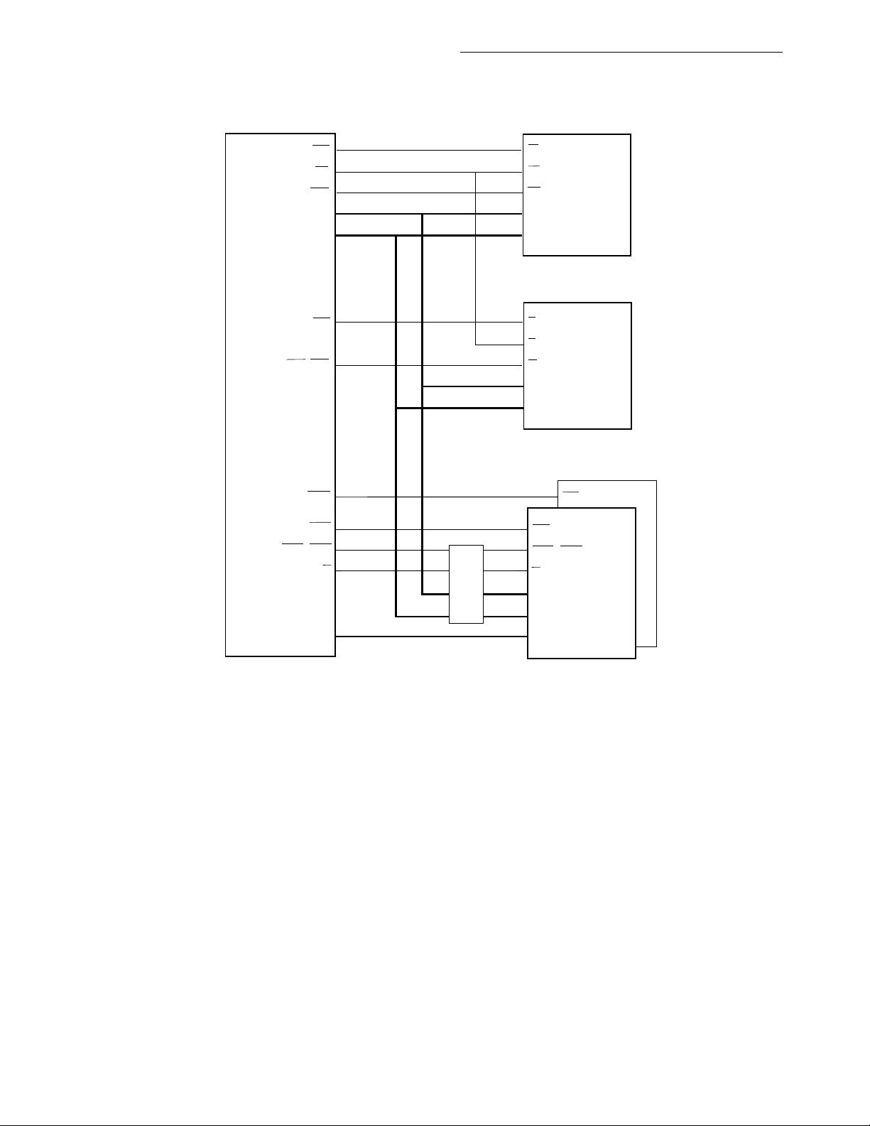
8-BIT BOOT
Introduction
QUICC
MC68360
CS0
OE
WE0
DATA
ADDRESS
CS7
WE3–WE0
RAS2
RAS1
CAS3–CAS0
R/W
PRTY3–PRTY0
BUFFER
EPROM
(FLASH OR REGULAR)
CE (ENABLE)
OE (OUTPUT ENABLE)
WE (WRITE)
DATA
ADDRESS
8-, 16-, OR 32-BIT SRAM
E (ENABLE)
G (OUTPUT ENABLE)
W (WRITE)
DATA
ADDRESS
16- OR 32-BIT
TWO DRAM SIMMs
(OPTIONAL PARITY)
RAS
RAS
CAS3–CAS0
W (WRITE)
DATA
ADDRESS
PARITY
Figure 1-3. Larger QUICC System Configuration
1.5 QUICC SERIAL CONFIGURATIONS
The QUICC offers an extremely flexible set of communications capabilities. Although a full
understanding of the possibilities requires reading the appropriate sections, some of the
possibilities are shown in the following diagrams. They show possible connections between
QUICC devices. In addition, connections are often shown between QUICCs and the
MC68302 to show the compatibility between these devices.
For readability, transceivers are usually omitted in the following diagrams. For local onboard communications, however, transceivers are often optional and depend on the protocol used.
Figure 1-4 shows the Ethernet LAN capability of the QUICC. An external SIA transceiver is
required to complete the interface to the media. This functionality is implemented in the
MC68160 enhanced Ethernet serial transceiver (EEST
MOTOROLA
MC68360 USER’S MANUAL
). The MC68160 EEST supports
1-9
Page 40

Introduction
connections to the attachment unit interface (AUI) or twisted-pair Ethernet formats and provides a glueless interface to the QUICC.
QUICC
SCC1
QUICC
SCC1
QUICC
SCC1
ETHERNET
MC68160
EEST
MC68160
EEST
MC68160
EEST
Figure 1-4. Ethernet LAN Capability
Figure 1-5 shows the AppleTalk LAN capability of the QUICC. Note that the MC68302
requires an extra device, the MC68195 LocalTalk adapter, to interface to AppleTalk.
QUICC
SCC
QUICC
SCC
MC68302
NOTE: The QUICC implements the AppleTalk LAN
protocol without the need for the MC68195.
SCC
MC68195
RS422
XCVR
RS422
XCVR
LA
RS422
XCVR
Figure 1-5. AppleTalk LAN Capability
Figure 1-6 shows the implementation of a LAN structure of HDLC called HDLC bus. This
protocol is the fastest, easiest way to interface multiple QUICCs in an HDLC-based protocol.
1-10
MC68360 USER’S MANUAL
MOTOROLA
Page 41

QUICC
SCC
QUICC
SCC
QUICC
SCC
NOTES:
1. HDLC bus—any node can obtain
mastership.
2. The QUICC handles collisions
without external glue.
HDLC BUS
Introduction
Figure 1-6. HDLC Bus LAN
Figure 1-7 shows the original SDLC application, which can be implemented by both QUICCs
and MC68302s.
QUICC
SCC
QUICC
SCC
MC68302
SCC
NOTE: No collisions are allowed in this
master-slave approach. Also
available on the MC68302.
SDLC BUS
Figure 1-7. FSDLC Bus Implementation
Figure 1-8 shows a UART LAN configuration that is supported by both the QUICC and the
MC68302, as well as many other industry UARTs.
MOTOROLA
MC68360 USER’S MANUAL
1-11
Page 42

Introduction
QUICC
SCC
QUICC
SCC
MULTI-DROP
UART
MC68302
SCC
NOTES:
1. Simple LAN based on UART mode.
2. Ninth bit is an "address" bit.
Figure 1-8. UART LAN Implementation
Figure 1-9 shows how the SPIs on the QUICC can be used to connect devices together into
a local bus. The SPI exists on many other Motorola devices, such as the MC68HC11 microcontroller, and a number of peripherals such as A/D and D/A converters, LED drivers, LCD
drivers, real-time clocks, serial EEPROM, PLL frequency synthesizers, and shift registers.
QUICC
MASTER/SLAVE
QUICC
MASTER/SLAVE
QUICC
MASTER/SLAVE
SPI
SPI
SPI
SPI BUS
1-12
NOTE: SPI bus configuration—each QUICC
can be the master in turn.
Figure 1-9. SPI Local Bus Implementation
MC68360 USER’S MANUAL
MOTOROLA
Page 43

Introduction
Figure 1-10 shows how the SCP on the MC68302 can be used to interface to the QUICC
SPI.
MC68302
SCP
MASTER
NOTE: The MC68302 SCP can communicate with the QUICC SPI.
SPI BUS
QUICC
SPI
SLAVE
EEPROMS
ETC.
SPI
SLAVE
Figure 1-10. SPI Implementation Using SCP
Figure 1-11 shows how the SPI on the QUICC can interface to another QUICC or SPI-based
peripherals.
QUICC
SPI
MASTER
SPI BUS
QUICC
SPI
SLAVE
EEPROMS
ETC.
SPI
SLAVE
NOTE: Two QUICCs configured for a master-slave SPI connection.
Figure 1-11. SPI Master-Slave Implementation
Figure 1-12 shows how the parallel interface port (PIP) can be used to implement the Centronics interface connection. The QUICC may be the peripheral or the host.
QUICC
PIP
NOTE: The QUICC can communicate over a Centronics Interface.
CENTRONICS
INTERFACE
8 DATA LINES
HOST
COMPUTER
OR PRINTER
Figure 1-12. Centronics Interface Implementation
MOTOROLA
MC68360 USER’S MANUAL
1-13
Page 44

HDLC/SDLC
Introduction
Figure 1-13 shows how the PIP can also be used to implement a fast parallel connection
between devices.
QUICC
PIP
NOTE: Fast parallel connection between QUICCs.
PARALLEL
INTERFACE
8 DATA LINES
QUICC
PIP
Figure 1-13. Fast Parallel Connection Implementation
Figure 1-14 shows which SCC protocols may be used to connect SCCs on the QUICC and
the MC68302.
QUICC MC68302
SCC
HDLC/SDLC
BISYNC
UART
TRANSPARENT
SCC
Figure 1-14. SCC Protocol Implementation
Figure 1-15 shows which SCC protocols may be used to connect SCCs on multiple QUICCs
or to other devices supporting such protocols.
QUICC QUICC
SCC SCC
NOTE: Point-to-point (WAN) configurations are available on the QUICC.
BISYNC UART
TRANSPARENT
SYNCHRONOUS UART
SS#7
Figure 1-15. Multiple QUICC Point-to-Point Implementation
Figure 1-16 shows other point-to-point options that are possible with the QUICC and the
MC68302.
1-14
MC68360 USER’S MANUAL
MOTOROLA
Page 45

QUICC MC68302
Introduction
QUICC
QUICC
SMC
SMC SCP
SMC
UART
TRANSPARENT
TRANSPARENT
UART
TRANSPARENT
SCC
MC68302
QUICC
SMC
Figure 1-16. Other Point-to-Point Implementations
Figure 1-17 shows how up to six of the serial channels can connect to a TDM interface. The
QUICC provides a built-in time-slot assigner for access to the TDM time slots. Other channels can work with their own set of pins, allowing possibilities like an Ethernet to T1 bridge,
etc.
QUICC
SCC
SCC
SCC
SCC
SMC
SMC
ANY COMBINATION OF SCCs
AND SMCs MAY BE
CONNECTED TO THE TDM.
NOTE: Independent receive and transmit clocking, routing,
and syncs are supported.
Figure 1-18 shows that the QUICC time-slot assigner can support two TDM buses. Each
Figure 1-17. Serial Channel to TDM Bus Implementation
TIME
SLOT
ASSIGNER
TIME DIVISION MULTIPLEXED BUS
T1, CEPT, IDL, GCI, ISDN,
PRIMARY RATE,
USER-DEFINED
TDM bus can be of a different format—for example, one TDM can be a T1 line, and one can
be a CEPT line. Also this technique could be used to bridge frames from basic rate ISDN to
a T1/CEPT line, etc.
MOTOROLA
MC68360 USER’S MANUAL
1-15
Page 46

Introduction
QUICC
SCC
SCC
SCC
SCC
SMC
SMC
ANY COMBINATION OF SCCs
AND SMCs MAY BE
CONNECTED TO ANY TDM.
NOTE: Two TDM buses may be simultaneously supported
with the time slot assigner.
TIME
SLOT
ASSIGNER
TDM BUS 1
TDM BUS 2
Figure 1-18. Dual TDM Bus Implementation
1.6 QUICC SERIAL CONFIGURATION EXAMPLES
Figure 1-19 shows a situation where multiple QUICCs can communicate over a TDM line.
This can be used, for instance, to implement an 8-channel line card. The SCCs implement
the line interfaces, and the SMCs provide the local on-board communication between the
QUICCs. The additional SMC on each QUICC can be used as a serial debug port. The SPI
can be used to interface to peripherals, such as a serial EEPROM.
TWO SMCs ARE
USED TO
COMMUNICATE
LOCALLY
BETWEEN QUICCs
OVER A TIME SLOT.
SCC
SCC
SCC
SCC
SMC
SMC
SCC
SCC
SCC
SCC
SMC
SMC
QUICC
QUICC
TIME
SLOT
ASSIGNER
TIME
SLOT
ASSIGNER
TDM BUS
1-16
NOTE: The eight SCCs and two SMCs support 10 time slots on the TDM bus.
The length and position of the time slots are made with time slot assigners.
Figure 1-19. Multiple QUICC TDM Bus Implementation
MC68360 USER’S MANUAL
MOTOROLA
Page 47

Introduction
Figure 1-20 shows a general-purpose application that includes Ethernet, AppleTalk, an
HDLC connection to a T1 line, an HDLC connection to frame relay, a UART debug monitor
port, a totally transparent data stream port, and an SPI connection to a serial EEPROM.
QUICC
SCC3
SCC1
SCC2
TIME
SLOT
ASSIGNER
SCC4
SMC1
UART
DEBUG
PORT
SERIAL
EEPROM
RS-232
SYSTEM
BUS
SPI
SMC2
Figure 1-20. General-Purpose Application
1.7 QUICC SYSTEM BUS CONFIGURATIONS
MOTOROLA
SIA
TRANSCEIVER
RS-422
T1 LINE
TRANSCEIVER
RS-232
RS-232
ETHERNET
APPLE TALK
X.25 (HDLC)
FRAME RELAY (HDLC)
TRANSPARENT DATA
Figure 1-21 shows a master-slave QUICC configuration. This system gives eight SCCs, four
SMCs, two SPIs, four IDMAs, etc. Each QUICC uses its own DMA capability, but the
CPU32+ is the only processor in the system. More QUICCs can be easily supported on the
system bus, if desired.
QUICC
MASTER
CPU32+
QUICC SYSTEM BUS
SCC
SCC
SCC
SCC
SMC
SMC
SPI
QUICC
SLAVE
CPU32+
SCC
SCC
SCC
SCC
SMC
SMC
SPI
MOTOROLA
Figure 1-21. Master-Slave QUICC Implementation
MC68360 USER’S MANUAL
1-17
Page 48

Introduction
The QUICC has special features in slave mode to support the M68040 family. When the
QUICC is used in this way, it is said to be in MC68040 companion mode. Figure 1-22 shows
how a QUICC in slave mode can interface to a MC68EC040. (The MC68EC040 is a lowcost version of the MC68040 with identical integer performance, but without the memory
management unit (MMU) and the floating-point unit (FPU).) The DRAM controller on the
QUICC will control the accesses of the MC68EC040 (including the burst modes). This configuration does require external address multiplexers, but the QUICC controls the multiplexers. The QUICC supports the MC68EC040 in other ways, such as interrupt handling and
system protection features. When it is in slave mode, the QUICC can also be interfaced to
any MC68030-type bus master instead of the MC68EC040.
MC68EC040
SYSTEM BUS
CONTROL
QUICC SLAVE
MC68EC040
SUPPORT
FUNCTIONS
MEMORY
CONTROLLER
EPROM
CPU32+
SCC
SCC
SCC
SCC
SMC
SMC
SPI
1-18
DRAM
ADDRESS
MUXs
SRAM
Figure 1-22. MC68040 Companion Mode
MC68360 USER’S MANUAL
MOTOROLA
Page 49

SECTION 2
SIGNAL DESCRIPTIONS
This section contains brief descriptions of the QUICC input and output signals in their functional groups as shown in Figure 2-1.
2.1 SYSTEM BUS SIGNAL INDEX
The QUICC system bus signals consist of two groups. The first group, listed in Table 2-1,
consists of system bus signals that exist when the QUICC is in the normal mode (CPU32+
enabled). The second group consists of system bus signals that exist when the QUICC is in
the slave mode (CPU32+ disabled). They are listed in Table 2-7 and may also be identified
in Figure 2-1 as those with an italic font. In Table 2-1, the signal name, mnemonic, and a
brief functional description are presented. For more detail on each signal, refer to the paragraphs that discuss each signal.
2.1.1 Address Bus
The address bus consists of the following two groups. Refer to Section 4 Bus Operation for
information on the address bus and its relationship to bus operation.
2.1.1.1 ADDRESS BUS (A27–A0). This three-state bidirectional bus (along with A31–A28)
provides the address for the current bus cycle, except in the CPU address space. Refer to
Section 4 Bus Operation for more information on the CPU address space. A27 is the most
significant address signal in this group.
2.1.1.2 ADDRESS BUS (A31–A28). These pins can be programmed as the most signifi-
cant four address bits or as four byte write enables.
A31–A28—These pins can function as the most significant 4 address bits. A31 is the
most significant address signal in this group.
–WE0—On a write cycle, these active-low signals indicates which byte of the 32-
WE3
bit data bus contains valid data.
WE0—Corresponds to A31 and selects data bits 31–24. Also may be referred to as UUWE.
—Corresponds to A30 and selects data bits 23–16. Also may be referred to as UM-
WE1
WE.
—Corresponds to A29 and selects data bits 15–8. Also may be referred to as LMWE.
WE2
—Corresponds to A28 and selects data bits 7–0. Also may be referred to as LLWE.
WE3
MOTOROLA
MC68360 USER’S MANUAL
2-1
Page 50

B
2
Signal Descriptions
Write enable does not have the capability to follow dynamic bus
sizing with external assertion of DSACK
ways follow the port size that is programed in GMR and the OR.
For more information see 6.10 Memory Controller.
NOTE
. Write enable will al-
ADDRESS BUS
PORT A
RXD1/PA0
TXD1/PA1
RXD2/PA2
TXD2/PA3
L1TXDB/RXD3/PA4
L1RXDB/TXD3/PA5
L1TXDA/RXD4/PA6
L1RXDA/TXD4/PA7
TIMERs/SCCs/SIs/CLOCKs/BRG
TIN1/L1RCLKA/BRGO1/CLK1/PA8
BRGCLK1/TOUT1/CLK2/PA9
TIN2/L1TCLKA/BRGO2/CLK3/PA10
RGCLK2/L1RCLKB/TOUT3/CLK6/PA13
RRJCT2/SPIMOSI(SPITXD)/PB2
BRGO4/SPIMISO(SPIRXD)/PB3
SDACK2/L1TSYNCB/CTS3/PC8
SDACK1/L1TSYNCA/CTS4/PC10
TOUT2/CLK4/PA11
TIN3/BRGO3/CLK5/PA12
TIN4/BRGO4/CLK7/PA14
L1TCLKB/TOUT4/CLK8/PA15
PORT B (PIP)
RRJCT1/SPISEL/PB0
RSTRT2/SPICLK/PB1
DREQ1/BRGO1/PB4
DACK1/BRGO2/PB5
DONE1/SMTXD1/PB6
DONE2/SMRXD1/PB7
DREQ2/SMSYN1/PB8
DACK2/SMSYN2/PB9
L1CLKOB/SMTXD2/PB10
L1CLKOA/SMRXD2/PB11
L1ST1/RTS1/PB12
L1ST2/RTS2/PB13
L1ST3/L1RQB/RTS3/PB14
L1ST4/L1RQA/RTS4/PB15
STRBO/BRGO3/PB16
STRBI/RSTRT1/PB17
PORT C (INTERRUPT PARALLEL I/O)
L1ST1/RTS1/PC0
L1ST2/RTS2/PC1
L1ST3/L1RQB/RTS3/PC2
L1ST4/L1RQA/RTS4/PC3
CTS1/PC4
TGATE1/CD1/PC5
CTS2/PC6
TGATE2/CD2/PC7
L1RSYNCB/CD3/PC9
L1RSYNCA/CD4/PC11
QUICC
MC68360
240 PINS
DATA BUS
BUS CONTROL
BUS ARBITRATION
SYSTEM CONTROL
INTERRUPT
MEMORY CONTROLLER
TEST
CLOCK
A27–A0
A31–A28/WE3–WE0
FC2–FC0/TM2–TM0
FC3/TT0
D31–D16
D15–D0
PRTY1–PRTY0/IOUT1–IOUT
PRTY2/IOUT0/RQOUT
PRTY3/16BM
SIZ0
SIZ1
DSACK0/TBI
DSACK1/TA
R/W
AS
DS/TT1
OE/AMUX
RMC/CONFIG0/LOCK
BR
BG
BGACK/BB
BCLRO/CONFIG1/RAS2DD
RESETH
RESETS
HALT
BERR/TEA
PERR
CONTROL
IRQ1/IOUT0/RQOUT
IRQ4/IOUT1
IRQ6/IOUT2
IRQ2,3,5,7
AVEC/IACK5/AVECO
CS6–CS0/RAS6–RAS0
CS/RAS7/IACK7
CAS3–CAS0/IACK6,3,2,1
TRIS/TS
BKPT/BKPTO/DSCLK
FREEZE/CONFIG2/MBARE
IPIPE1/RAS1DD/BCLRI
IPIPE0/BADD2/DSO
IFETCH/BADD3/DSI
TCK
TMS
TDI
TDO
TRST
XTAL
EXTAL
XFC
MODCK1–MODCK0
CLKO2–CLKO1
2-2
Figure 2-1. QUICC Functional Signal Groups
MC68360 USER’S MANUAL
MOTOROLA
Page 51

Table 2-1. System Bus Signal Index (Normal Operation)
Group Signal Name Mnemonic Function
Address Address Bus A27–A0 Lower 27 bits of address bus. (I/O)
Address Bus/Byte
Write Enables
Function Codes FC3–FC0
Data Data Bus 31–16 D31–D16
Data Bus 15–0 D15–D0
Parity Parity 2–0 PRTY2–PRTY0
Parity3/16BM
A31–A28/
–WE3
WE0
PRTY3/16BM
Upper four bits of address bus (I/O), or byte write enable signals (O) for accesses to external memory or peripherals.
Identifies the processor state and the address space of the
current bus cycle. (I/O)
Upper 16-bit data bus used to transfer byte or word data.
Used in 16-bit bus mode (I/O).
Lower 16-bit data bus used to transfer 3-byte or long-word
data (I/O). Not used in 16-bit bus mode.
Parity signals for byte writes/reads from/to external memory
module (I/O).
Parity signals for byte writes/reads from/to external memory
module or defines 16-bit bus mode. (I/O)
Signal Descriptions
Parity Error PERR
Memory
Controller
Bus Arbitration Bus Request BR
Bus Control
Interrupt
Control
Chip Select/Row Address Select 7/
Interrupt Acknowledge 7
Chip Select 6–0/
Row Address Select
6–0
Column Address Select 3–0/Interrupt Acknowledge 1, 2, 3, 6
Bus Grant BG
Bus Grant Acknowl-
edge
Read-Modify-Write
Cycle/Initial Configuration 0
Bus Clear Out/
Initial Configuration
1/Row Address Select 2 Double-Drive
Data and Size Acknowledge
Address Strobe AS
Data Strobe DS
Size SIZ1–SIZ0
Read/Write R/W
Output Enable/
Address Multiplex
Interrupt Request
Level 7–1
Autovector/Interrupt
Acknowledge 5
/RAS7/IACK7
CS
CS6
RAS6
CAS3
IACK6
BGACK
/CONFIG0
RMC
BCLRO
RAS2DD
DSACK1
OE
IRQ7
AVEC
–CS0/
–RAS0
-CAS0/
/CONFIG1/
–DSACK0
/AMUX
–IRQ1
/IACK5
Indicates a parity error during a read cycle. (O)
Enables peripherals or DRAMs at programmed addresses
(O) or interrupt level 7 acknowledge line (O).
Enables peripherals or DRAMs at programmed addresses.
(O)
,3,2,1
Indicates the direction of data transfer on the bus. (I/O)
DRAM column address select or interrupt level acknowledge
lines. (O)
Indicates that an external device requires bus mastership. (I)
Indicates that the current bus cycle is complete and the
QUICC has relinquished the bus. (O)
Indicates that an external device has assumed bus master-
ship. (I)
Identifies the bus cycle as part of an indivisible read-modify-
write operation (I/O) or initial QUICC configuration select (I).
Indicates that an internal device requires the external bus
(Open-Drain O) or initial QUICC configuration select (I) or
row address select 2 double-drive output (O).
Provides asynchronous data transfer acknowledgement and
dynamic bus sizing (open-drain I/O but driven high before
three-stated).
Indicates that a valid address is on the address bus. (I/O)
During a read cycle, DS indicates that an external device
should place valid data on the data bus. During a write cycle,
indicates that valid data is on the data bus. (I/O)
DS
Indicates the number of bytes remaining to be transferred for
this cycle. (I/O)
Active during a read cycle indicates that an external device
should place valid data on the data bus (O) or provides a
strobe for external address multiplexing in DRAM accesses
if internal multiplexing is not used (O).
Provides external interrupt requests to the CPU32+ at priority levels 7–1. (I)
Autovector request during an interrupt acknowledge cycle
(open-drain I/O) or interrupt level 5 acknowledge line (O).
MOTOROLA
MC68360 USER’S MANUAL
2-3
Page 52

Signal Descriptions
Table 2-1. System Bus Signal Index (Normal Operation)(Continued)
)
Group Signal Name Mnemonic Function
System
Control
Clock and Test System Clock Out 1 CLKO1 Internal system clock output 1. (O)
Clock and Test
(Cont'd)
Power
— No Connect NC4–NC1 Four no-connect pins.
Soft Reset RESETS
Hard Reset RESETH
Halt HALT
Bus Error BERR
System Clock Out 2 CLKO2 Internal system clock output 2—normally 2x CLKO1. (O)
Crystal Oscillator
External Filter Ca-
pacitor
Clock Mode Select
1–0
Instruction Fetch/
Development Serial
Input
Instruction Pipe 0/
Development Serial
Output
Instruction Pipe 1/
Row Address Select
1 Double-Drive
Breakpoint/
Development Serial
Clock
Freeze/Initial Configuration 2
Three-State TRIS
Test Clock TCK Provides a clock for Scan test logic. (I)
Test Mode Select TMS Controls test mode operations. (I)
Test Data In TDI Serial test instructions and test data signal. (I)
Test Data Out TDO Serial test instructions and test data signal. (O)
Test Reset TRST
Clock Synthesizer
Power
Clock Synthesizer
Ground
Clock Out Power VCCCLK Power supply to clock out pins.
Clock Out Ground GNDCLK Ground supply to clock out pins.
Special Ground 1 GNDS1
Special Ground 2 GNDS2
System Power Sup-
ply and Return
EXTAL,
XTAL
XFC
MODCK1–MODCK0
IFETCH
IPIPE0
IPIPE1
BKPT
/DSI
/DSO
/RAS1DD
/DSCLK
FREEZE/
CONFIG2
VCCSYN Power supply to the PLL of the clock synthesizer.
GNDSYN Ground supply to the PLL of the clock synthesizer.
VCC, GND Power supply and return to the QUICC.
Sft system reset. (open-drain I/O)
Hard system reset. (open-drain I/O)
Suspends external bus activity. (open-drain I/O)
Indicates an erroneous bus operation is being attempted.
(open-drain I/O)
Connections for an external crystal to the internal oscillator
circuit. EXTAL (I), XTAL (O).
Connection pin for an external capacitor to filter the circuit of
the PLL (I).
Selects the source of the internal system clock. (I) THESE
PINS SHOULD NOT BE SET TO 00
Indicates when the CPU32+ is performing an instruction
word prefetch (O) or input to the CPU32+ background debug
mode (I).
Used to track movement of words through the instruction
pipeline (O) or output from the CPU32+ background debug
mode (O).
Used to track movement of words through the instruction
pipeline (O), or a row address select 1 “double-drive” output
(O).
Signals a hardware breakpoint to the QUICC (open-drain I/
O), or clock signal for CPU32+ background debug mode (I).
Indicates that the CPU32+ has acknowledged a breakpoint
(O), or initial QUICC configuration select (I).
Used to three-state all pins if QUICC is configured as a master. Sampled during system reset. (I)
Provides an asynchronous reset to the test controller. (I)
Special ground for fast AC timing on certain system bus signals.
Special ground for fast AC timing on certain system bus signals.
NOTE: I denotes input, 0 denotes output, and I/O is input/output.
2-4
MC68360 USER’S MANUAL
MOTOROLA
Page 53

Signal Descriptions
2.1.2 Function Codes (FC3–FC0)
These three-state bidirectional signals identify the processor state and the address space
of the current bus cycle as noted in Table 2-2. The function code pins provide the purpose
of each bus cycle to external logic.
Other bus masters besides the QUICC may also output function codes during their bus
cycles. On the QUICC, this capability is provided for each potential internal bus master (i.e.,
the IDMA, SDMA, and DRAM refresh units). Provision is also made for the decoding of function codes that are output from external bus masters (e.g., in the memory controller chipselect generation logic).
In computer design, function code information can be used to protect certain portions of the
address map from unauthorized access or to extend the addressable range beyond the
address limit. However, in controller applications, function codes are most often used as a
debugging aid. Furthermore, in most controller applications, the QUICC stays continuously
in the supervisor state.
Refer to Section 4 Bus Operation for more information.
Table 2-2. Address Space Encoding
Function Code Bits
3210 Address Space
0000Reserved (Motorola)
0001User Data Space
0010User Program Space
0011Reserved (User)
0100Reserved (Motorola)
0101Supervisor Data Space
0110Supervisor Program Space
0111Supervisor CPU Space
1 x x x DMA Space
NOTE
FC3-0 may not be set to 0xF
2.1.3 Data Bus
The data bus consists of the following two groups. Refer to Section 4 Bus Operation for information on the data bus and its relationship to bus operation.
2.1.3.1 DATA BUS (D31–D16). These three-state bidirectional signals (along with D15–
D0) provide the general-purpose data path between the QUICC and all other devices.
Although the data path is a maximum of 32 bits wide, it can be dynamically sized to support
8-, 16-, or 32-bit transfers. D31 is the MSB of the data bus. Byte and word operations occur
on D31–D16. Additionally, if the QUICC is configured into 16-bit bus mode, the D31–D16
MOTOROLA
MC68360 USER’S MANUAL
2-5
Page 54

Signal Descriptions
pins are the only data pins used. Refer to Section 4 Bus Operation for information on the
data bus and its relationship to bus operation.
2.1.3.2 DATA BUS (D15–D0). These pins can function as 16 additional data pins used in
long-word and 3-byte transfers. They are three-stated and not used if the QUICC is configured into 16-bit bus mode.
2.1.4 Parity
These three-state bidirectional signals provide parity generation/checking for the data path
between the QUICC or external masters and other devices. There are four parity lines—one
for every eight data bits. The parity lines consists of two groups. Refer to Section 6 System
Integration Module (SIM60) for more information on parity generation/checking.
2.1.4.1 PARITY (PRTY0). This pin is the parity value for data bits 31–24.
2.1.4.2 PARITY (PRTY1). This pin is the parity value for data bits 23–16.
2.1.4.3 PARITY (PRTY2). This pin is the parity value for data bits 15–8.
2.1.4.4 PARITY (PRTY3). This pin has two functions. During total system reset, it is the
16BM
pin to determine whether 16-bit data bus mode is to be enabled. After system reset,
it functions as the parity line 3.
PRTY3—This pin is the parity value for data bits 0–7.
16BM
—This pin selects the 16-bit data bus mode. To choose a 32-bit data bus during total
system reset, this pin can be left floating (it has an internal pullup resistor) or can be driven/
pulled high. To choose a 16-bit data bus during total system reset, this pin should be driven/
pulled low.
2.1.5 Memory Controller
The following signals are used to control an external memory device.
2.1.5.1 CHIP SELECT/ROW ADDRESS SELECT (CS6–CS0/RAS6–RAS0). The chip-
select output signals enable peripherals or memory arrays at programmed addresses. CS0
is the global chip select for the boot ROM containing the user’s reset vector and initialization
program. Refer to Section 6 System Integration Module (SIM60) for more information on
chip selects.
NOTE
In addition, RAS1 can be simultaneously output on the RAS1DD
pin to increase the RAS1 line drive capability, and RAS2 can be
simultaneously output on the RAS2DD
pin to increase the RAS2
line drive capability.
2.1.5.2 CHIP SELECT/ROW ADDRESS SELECT/INTERRUPT ACKNOWLEDGE (CS7/
RAS7
/IACK7). This pin can be programmed as a CS7/RAS7 pin or as the IACK7 line. See
Section 6 System Integration Module (SIM60) for more information on this selection.
2-6
MC68360 USER’S MANUAL
MOTOROLA
Page 55

RAS7/CS7—Row address select 7 or chip select 7 output signal.
Signal Descriptions
IACK7
rupt acknowledge cycle. Peripherals can use the IACKx
address bus and function codes to determine that an interrupt acknowledge cycle is in
progress and to obtain the current interrupt level. IACKx
vector is generated internally by the QUICC. See Section 4 Bus Operation for more information.
2.1.5.3 COLUMN ADDRESS SELECT/INTERRUPT ACKNOWLEDGE (CAS3–CAS0/
IACK6
DRAMs or as interrupt acknowledge lines.
CAS3
umns:
IACK1
of an external interrupt during an interrupt acknowledge cycle. Peripherals can use the
IACKx
an interrupt acknowledge cycle is in progress and to obtain the current interrupt level. IACKx
lines need not be used when the vector is generated internally by the QUICC. See Section
4 Bus Operation for more information.
—The QUICC asserts this pin to indicate a level 7 external interrupt during an inter-
strobes instead of monitoring the
lines need not be used when the
, 3, 2, 1). These pins can be programmed as four column address selects for
–CAS0—The DRAM column address select output signal enables the DRAM col-
CAS0 selects data bits 31–24.
CAS1
CAS2
CAS3
selects data bits 23–16.
selects data bits 15–8.
selects data bits 7–0.
, IACK2, IACK3, IACK6—The QUICC asserts one of these pins to indicate the level
strobes instead of monitoring the address bus and function codes to determine that
IACK1 corresponds to CAS0.
IACK2
IACK3
IACK6
2.1.5.4 ADDRESS MULTIPLEX (AMUX). See 2.1.7.7 Output Enable/Address Multiplex
(OE/AMUX) for more information.
2.1.6 Interrupt Request Level (
These pins are prioritized interrupt request lines. IRQ7, the highest priority, is nonmaskable;
IRQ6
mation on the interrupt request lines.
corresponds to CAS1.
corresponds to CAS2.
corresponds to CAS3.
IRQ7
–
IRQ1
)
–IRQ1 are internally maskable interrupts. Refer to Section 5 CPU32+ for more infor-
2.1.7 Bus Control Signals
These signals control the bus transfer operations of the QUICC. Refer to Section 4 Bus
Operation for more information on these signals.
MOTOROLA
MC68360 USER’S MANUAL
2-7
Page 56

Signal Descriptions
2.1.7.1 DATA AND SIZE ACKNOWLEDGE (DSACK1–DSACK0). These two active-low
bidirectional signals allow asynchronous data transfers and dynamic data bus sizing
between the QUICC and external devices (see Table 2-3).
Table 2-3. DSACKx Encoding
DSACK1 DSACK0 Result
1 (Negated) 1 (Negated) Insert wait states in current bus cycle.
1 (Negated) 0 (Asserted) Complete cycle—data bus port size is 8 bits.
0 (Asserted) 1 (Negated) Complete cycle—data bus port size is 16 bits.
0 (Asserted) 0 (Asserted) Complete cycle—data bus port size is 32 bits.
2.1.7.2 AUTOVECTOR/INTERRUPT ACKNOWLEDGE (AVEC/IACK5). This pin can be
programmed to be an autovector input or the interrupt acknowledge 5 line output.
AVEC
—This signal requests an automatic vector during an interrupt acknowledge cycle.
Refer to Section 6 System Integration Module (SIM60) for more information on the autovector function. AVEC
IACK5
—The QUICC asserts this pin to indicate the level of an external interrupt during an
interrupt acknowledge cycle at level 5. Peripherals can use the IACKx
need not be used if the QUICC supplies the vector internally.
strobes instead of
monitoring the address bus and function codes to determine that an interrupt acknowledge
cycle is in progress and to obtain the current interrupt level. IACKx
lines need not be used
when the vector is generated internally by the QUICC.
2.1.7.3 ADDRESS STROBE (AS). This bidirectional signal is driven by the bus master to
indicate a valid address on the address bus. The function code, size, and read/write signals
are also valid when AS
is asserted.
2.1.7.4 DATA STROBE (DS). During a read cycle, this input/output signal is driven by the
bus master to indicate that an external device should place valid data on the data bus. During a write cycle, the data strobe indicates that valid data is on the data bus.
2.1.7.5 TRANSFER SIZE (SIZ1, SIZ0). These bidirectional signals are driven by the bus
master to indicate the number of operand bytes remaining to be transferred in the current
bus cycle (see Table 2-4).
Table 2-4. SIZx Encoding
SIZ1 SIZ0 Transfer Size
0 1 Byte
1 0 Word
1 1 3 Bytes
0 0 Long Word
2.1.7.6 READ/WRITE (R/W). This active-high bidirectional signal is driven by the bus mas-
ter to indicate the direction of data transfer on the bus. A logic one indicates a read from a
slave device; a logic zero indicates a write to a slave device.
2-8
MC68360 USER’S MANUAL
MOTOROLA
Page 57

Signal Descriptions
2.1.7.7 OUTPUT ENABLE/ADDRESS MULTIPLEX (OE/AMUX). This pin can be pro-
grammed as the output enable (OE
—During a read cycle, this output signal is driven by the bus master to indicate that an
OE
external device should place valid data on the data bus. OE
inversion of the R/W
signal.
) output or as the address multiplex output.
may used to save an external
AMUX—This output signal is driven by the DRAM controller to the external address multiplexer. AMUX need not be used if the DRAM addresses are multiplexed internally by the
QUICC.
2.1.7.8 BYTE WRITE ENABLE (WE3–WE0) . See 2.1.1.2 Address Bus (A31–A28) for the
description.
2.1.8 Bus Arbitration Signals
The following signals are the four bus arbitration control signals used to determine the bus
master. Refer to Section 4 Bus Operation for more information concerning these signals.
2.1.8.1 BUS REQUEST (BR). This active-low input signal indicates that an external device
needs to become the bus master. This input is typically wire-ORed.
2.1.8.2 BUS GRANT (BG). Assertion of this active-low output signal indicates that the bus
master has relinquished the bus.
2.1.8.3 BUS GRANT ACKNOWLEDGE (BGACK). Assertion of this active-low input indi-
cates that an external device has become the bus master.
2.1.8.4 READ-MODIFY-WRITE CYCLE/INITIAL CONFIGURATION (RMC/CONFIG0).
This pin can be programmed as the read-modify-write cycle output or as the initial configuration pin 0 input signal during system reset.
—This output signal identifies the bus cycle as part of an indivisible read-modify-write
RMC
operation; it remains asserted during all bus cycles of the read-modify-write operation to
indicate that bus ownership cannot be transferred.
NOTE
RMC is muxed with a CONFIG0 pin. RMC only functions when
the CPU32+ is enabled, and is an output unless an external
master ownes the bus, in which case it is an input.
CONFIG0—See 2.1.13 Initial Configuration Pins (CONFIG) for the description.
2.1.8.5 BUS CLEAR OUT/INITIAL CONFIGURATION/ROW ADDRESS SELECT
DOUBLE-DRIVE (BCLRO
/CONFIG1/RAS2DD). This pin can be programmed as the bus
clear out output or as the initial configuration pin 1 input signal during system reset or as the
RAS2DD
MOTOROLA
output double-drive signal.
MC68360 USER’S MANUAL
2-9
Page 58

Signal Descriptions
BCLRO—This active-low open-drain output indicates that one of the QUICC internal bus
masters is requesting the external bus master to release the bus.
CONFIG1—See 2.1.13 Initial Configuration Pins (CONFIG) for the description.
RAS2
—See 2.1.5.1 Chip Select/Row Address Select (CS6–CS0/RAS6–RAS0) for the
description.
2.1.9 System Control Signals
The QUICC uses these signals to recover from an exception. Refer to Section 4 Bus Operation for more information on these signals.
2.1.9.1 SOFT RESET (RESETS). This active-low, open-drain, bidirectional signal is used to
initiate reset. An external reset signal (as well as a reset from the SIM60) resets the QUICC
as well as all external devices. A reset signal from the CPU32+ (asserted as part of the
RESET instruction) resets external devices only—the internal state of the CPU32+ is not
affected; other on-chip modules are reset, but the configuration is not altered. When
asserted by the QUICC, this signal is guaranteed to be asserted for a minimum of 512 clock
cycles. For more information see 4.7 Reset Operation.
2.1.9.2 HARD RESET (RESETH). This active-low, open-drain, bidirectional signal is used
to initiate reset. An external hard reset signal (as well as an hard reset from the SIM60)
resets the QUICC as well as all external devices and the internal state of the CPU32+; other
on-chip modules are reset as well as the QUICC configuration. When asserted by the
QUICC, this signal is guaranteed to be asserted for a minimum of 512 clock cycles. For more
information see 4.7 Reset Operation.
During a hard reset, the address, data, and bus control pins are all three-stated. The BG
output is the same as that on the BR
input. The general-purpose I/O pins are all configured
pin
as inputs. The NC4–NC1 pins are undefined outputs. The XTAL, CLKO1, and CLKO2 pins
are active outputs, except for CLKO1 which does not oscillate while the on-chip PLL is
attaining a lock. The RESETS
pin is an output.
2.1.9.3 HALT (HALT). This active-low, open-drain, bidirectional signal is asserted to sus-
pend external bus activity, to request a retry when used with BERR
step operation. As an output, HALT
indicates a double bus fault by the CPU32+.
, or to perform a single-
2.1.9.4 BUS ERROR (BERR). This active-low, open-drain, bidirectional signal indicates
that an invalid bus operation is being attempted or, when used with HALT
, that the bus mas-
ter should retry the current cycle.
2.1.10 Clock Signals
These signals are used by the QUICC for controlling or generating the system clocks. Refer
to Section 6 System Integration Module (SIM60) for more information on these clock signals.
2.1.10.1 SYSTEM CLOCK OUTPUTS (CLKO2–CLKO1). These output signals reflect the
general system clock and are used as the bus timing reference by external devices. CLKO1
2-10
MC68360 USER’S MANUAL
MOTOROLA
Page 59

×
Signal Descriptions
is the general system clock. CLKO2 is 2 × CLKO1 if the on-chip clock synthesizer PLL is
used, and is 1
CLKO1 otherwise.
2.1.10.2 CRYSTAL OSCILLATOR (EXTAL, XTAL). These two pins are the connections
for an external crystal to the internal oscillator circuit. If an external oscillator is used, it
should be connected to EXTAL, with XTAL left open.
2.1.10.3 EXTERNAL FILTER CAPACITOR (XFC). This pin is used to add an external
capacitor to the filter circuit of the PLL. The capacitor should be connected between XFC
and VCCSYN.
2.1.10.4 CLOCK MODE SELECT (MODCK1–MODCK0). The state of these active-high
input signals during reset selects the type of external clock that is used by the PLL in the
clock synthesizer to generate the system clocks. Table 2-5 lists the default values of the
PLL.
Table 2-5. Default Operation Mode of the PLL
MODCK
1–0 PLL
1
00
01 Enabled No 1 >10 MHz =EXTAL =EXTAL
10 Enabled Yes 401 4.192 MHz 32.75 kHz 13.14 MHz
11 Enabled No 401 32.768 kHz 32.768 kHz 13.14 MHz
1
This mode is reserved.
Disabled Reserved Reserved Reserved Reserved Reserved
Prescaled by
128
Multi. Factor
(MF + 1)
EXTAL Freq.
(examples)
CLKIN to the
PLL
Initial Freq.
(VCO/2)
2.1.11 Instrumentation and Emulation Signals
These signals are used for test or software debugging. Refer to Section 5 CPU32+ for more
information on these signals.
2.1.11.1 INSTRUCTION FETCH/DEVELOPMENT SERIAL INPUT (IFETCH/DSI). This
active-low output signal indicates when the CPU32+ is performing an instruction word
prefetch and when the instruction pipeline has been flushed. Additionally, this signal is the
serial input to the CPU32+ in its background debug mode to issue background commands,
etc.
2.1.11.2 INSTRUCTION PIPE/DEVELOPMENT SERIAL OUTPUT (IPIPE0/DSO). This
active-low output signal is used to track movement of words through the instruction pipeline.
Additionally, this signal is the serial output from the CPU32+ in its background debug mode
to issue background status, etc.
2.1.11.3 INSTRUCTION PIPE/ROW ADDRESS SELECT DOUBLE-DRIVE (IPIPE1/
RAS1DD). This active-low output signal is used to track movement of words through the
instruction pipeline. This signal also functions as a second output of the RAS1
signal to
increase fanout capability.
2.1.11.4 BREAKPOINT/DEVELOPMENT SERIAL CLOCK (BKPT
/DSCLK). This active-
low input signal is used to signal a hardware breakpoint to the CPU32+. Additionally, this
MOTOROLA
MC68360 USER’S MANUAL
2-11
Page 60

Signal Descriptions
signal is the serial clock used to transfer commands/status to and from the CPU32+ during
background debug mode.
2.1.11.5 FREEZE/INITIAL CONFIGURATION (FREEZE/CONFIG2). This pin can be programmed as the freeze output or as the initial configuration pin 2 input signal during system
reset.
FREEZE—Assertion of this active-high output signal indicates that the CPU32+ has
acknowledged a breakpoint and has initiated background mode operation.
CONFIG2—See 2.1.13 Initial Configuration Pins (CONFIG) for the description.
2.1.12 Test Signals
The following signals are used with the on-board test logic . See Section 8 Scan Chain Test
Access Port for more information on the use of these signals.
2.1.12.1 TRI-STATE SIGNAL (TRIS
only when the CPU32+ is enabled, and it is not sampled during reset. When asserted, TRIS
immediately tristates the pins.
2.1.12.2 TEST RESET (TRST
2.1.12.3 TEST CLOCK (TCK). This input provides a clock for on-board test logic.
2.1.12.4 TEST MODE SELECT (TMS). This input controls test mode operations for on-
board test logic.
2.1.12.5 TEST DATA IN (TDI). This input is used for serial test instructions and test data
for on-board test logic.
2.1.12.6 TEST DATA OUT (TDO). This output is used for serial test instructions and test
data for on-board test logic.
). This input provides asynchronous reset to the test logic.
). TThe TRIS pin is enabled as a tristate control pin
2.1.13 Initial Configuration Pins (CONFIG)
The CONFIG2–CONFIG0 pins select the QUICC initial configuration during reset (see Table
2-6). They decide whether the CPU32+ core will be enabled or disabled, the global chip
select port will be 8-, 16-, or 32-bits, and the MBAR address will be $003FF00 or
$0033FF04. After reset, these pins may be programmed to their other function. The
CONFIG2–CONFIG0 lines have internal pullup resistors so that if they are left floating, the
default selection will be 111. See Section 6 System Integration Module (SIM60) for more
information.
2-12 MC68360 USER’S MANUAL MOTOROLA
Page 61
Signal Descriptions
Table 2-6. Initial Configuration
Configuration Pins
CONFIG2/
FREEZE
0 0 0 Slave mode; global CS 8-bit size; MBAR at $003FF00.
001
0 1 0 Slave mode; global CS 16-bit size; MBAR at $003FF00.
011
1 0 0 CPU enabled; global CS 32-bit size; MBAR at $003FF00.
1 0 1 CPU enabled; global CS 16-bit size; MBAR at $003FF00.
1 1 0 Slave mode; global CS disabled; MBAR at $003FF04.
1 1 1 CPU enabled; global CS 8-bit size; MBAR at $003FF00. (Default)
CONFIG1/
BCLRO
CONFIG0/
RMC
Result
Slave mode; global CS 32-bit size; MBAR at $003FF00; not MC68040 companion mode; BR
MC68040 companion mode; global CS 32-bit size; MBAR at $003FF00; BR
input, BG
output.
output, BG input.
NOTE
All CONFIG pins do have an internal pull-up resistor during reset. If a configuration other than the default (CONFIG2-1 = 111)
is desired, these pins should be driven by an active open collector device during the assertion of RESETH.
2.1.14 Power Signals
The following signals are used for power and ground to the QUICC.
2.1.14.1 VCCSYN AND GNDSYN. These pins provide power and ground to the clock synthesizer. They should be bypassed to each other with a 0.1-µF capacitor. See the system
clock generation description in Section 6 System Integration Module (SIM60) for more
details.
2.1.14.2 VCCCLK AND GNDCLK. These pins provide power and ground to the clock output pins (CLKO1 and CLKO2). They should be bypassed to each other with a 0.1-µF capacitor. See the system clock generation description in Section 6 System Integration Module
(SIM60) for more detail.
2.1.14.3 GNDS1 AND GNDS2. These two pins are special ground pins that, if used properly, allow more aggressive timing to be provided on certain system bus pins. These pins
include AS
aggressive timing; the user does not need to modify any values in the section. GNDS1 and
GNDS2 should be connected to a quiet ground source or to a low-noise ground plane.
2.1.14.4 VCC AND GND. These pins are the rest of the power and ground connections for
the QUICC.
, CASx, and IPIPE. Section 10 Electrical Characteristics already shows the
2.1.14.5 NC4–NC1. These four pins should not be connected on the QUICC package. They
are reserved for future enhancements.
MOTOROLA MC68360 USER’S MANUAL 2-13
Page 62

Signal Descriptions
2.2 SYSTEM BUS SIGNAL INDEX IN SLAVE MODE
The CONFIG2–CONFIG0 pins are used to cause the QUICC to enter the slave mode. The
signal name, mnemonic, and a brief functional description are presented in Table 2-7. The
rest of the QUICC pins maintain their functionality in slave mode. See Section 4 Bus Operation for details.
Additionally, the QUICC provides special support for the MC68EC040 bus (or other
MC68040 family members) during slave mode. The MC68EC040 signals are marked in
boldface in the table. For more information on MC68EC040 bus operation, see M68040UM/
M68040 User's Manual
AD,
Operation and Section 6 System Integration Module (SIM60).
Table 2-7. System Bus Signal Index (Slave Mode)
. The QUICC MC68EC040 support is described in Section 4 Bus
Master Mode
Mnemonic
FC2–FC0
FC3
DS
DSACK1
DSACK0
BERR
TRIS
IPIPE0
/IFETCH Burst Address BADD3–BADD2
BR
BG
BGACK
/CONFIG0
RMC
Breakpoint Out BKPTO Signals a hardware breakpoint to the external CPU. (O)
BKPT
FREEZE/
CONFIG2
,4,6
IRQ1
Slave Mode
Signal Name
Function Codes/
Transfer Modifier
Function Code/
Transfer Type
Data Strobe/
Transfer Type
Data and Size Ac-
knowledge/
Transfer Acknowl-
edge
Data and Size Ac-
knowledge/
Transfer Burst In-
hibit
Bus Error/
Transfer Error
Acknowledge
Transfer Start TS Indicates the beginning of an MC68040 bus transfer. (I)
Bus Request
Bus Grant
Bus Grant Acknowl-
edge
Bus Busy
040 Lock Cycle/
Configuration 0
Freeze/Initial
Configuration Pin 2
Interrupt Request/
Interrupt Outputs
Slave Mode
Mnemonic Slave Mode Function
FC2–FC0/
TM2–TM0
FC3/TT0
DS
DSACK1
DSACK0
TBI
BERR
TEA
BR
BR
BG
BG
BGACK
BB
LOCK
CONFIG0
MBARE
CONFIG2
IRQ6
IOUT2
IRQOUT
/TT1
,4,1/
–IOUT0/
Identifies the processor state and the address space of the current bus cycle (I/O), or indicates the MC68EC040 supplement
information about the access (I).
Identifies the DMA address space of the current bus cycle (I/O),
or indicates the MC68EC040 general transfer type: normal,
MOVE16, alternate logical function code, and acknowledge
(I).
Data strobe (I/O), or indicates the MC68EC040 general transfer type: normal, MOVE16, alternate logical function code,
and acknowledge (I).
Provides asynchronous data transfers and dynamic bus sizing;
/TA
for the MC68EC040, asserted to acknowledge bus transfer.
(Both are open-drain I/O but driven high before three-stated.)
Provides asynchronous data transfers and dynamic bus sizing;
/
for the MC68EC040, indicates that a slave cannot handle a
line burst access. (Both are open-drain I/O but driven high be-
fore three-stated.)
BERR indicates an erroneous bus operation is being attempted
/
by the QUICC (open-drain I/O); TEA indicates the same for
the MC68EC040 (open-drain I/O)
Address lines 2,3 generated by the QUICC on behalf of the
MC68EC040, for MC68EC040 burst memory cycles. (O)
Asserted by the QUICC to request bus mastership (O.D. O), or
bus request input from the MC68040. (I)
Asserted by external logic to grant bus mastership to the QUICC
(I), or bus grant output to the MC68040. (O)
Indicates that an external device or the QUICC has assumed
bus mastership. (Open-drain I/O but driven high before threestated).
An MC68040 LOCK
/
obtaining the system bus during locked cycles (I), and the
initial QUICC configuration select (I).
/
Provides an MBAR access enable (I), or the initial QUICC configuration select. (I)
Provides an interrupt request to the QUICC interrupt controller
(I), or interrupt output signals (O) (either RQOUT
quest or IOUT2
signal input to prevent the QUICC from
–IOUT0 encoded).
as a single re-
2-14 MC68360 USER’S MANUAL MOTOROLA
Page 63

Signal Descriptions
Table 2-7. System Bus Signal Index (Slave Mode) (Continued)
Master Mode
Mnemonic
PRTY0
PRTY1
PRTY2
/IACK5 Autovector Output AVECO
AVEC
IPIPE1/
RAS1DD
Slave Mode
Signal Name
Parity 0/Interrupt Out-
put 2
Parity 1/Interrupt Out-
put 1
Parity 2/
Interrupt Output 0/
Request Output
Bus Clear Input/
Row Address Select 1
Double-Drive
Slave Mode
Mnemonic Slave Mode Function
PRTY0/IOUT2
PRTY1/IOUT1
PRTY2/IOUT0
RQOUT
BCLRI
RAS1DD
Parity signals for D31–D24 writes/reads from/to external memory bank (I/O), or interrupt output 2 signal (O).
Parity signals for D23–D16 writes/reads from/to external memory bank (I/O) or interrupt output 1 signal. (O)
Parity signals for D15–D8 writes/reads from/to external memory
/
bank (I/O), or interrupt output 0 signal (O), or RQOUT
gle interrupt request output (O).
Signal output to the external processor to generate an internal
vector number during an interrupt acknowledge cycle. (threestated O)
/
Signals that an external device requests the QUICC to release
the external bus (I), or row address select 1 double-drive (O).
as a sin-
2.3 ON-CHIP PERIPHERALS SIGNAL INDEX
The input and output system signals for the QUICC peripherals are listed in Table 2-8. The
signal name, mnemonic, and a brief functional description are presented. For more detail on
each signal, refer to the specific module section. The peripherals pins are divided into three
ports: A, B, and C.
Port A has 16 pins, port B has 18 pins, and port C has 12 pins. All the following signals are
multiplexed with either port A, B, or C. All pins may be inputs or outputs; in addition, some
pins may be configured to be open-drain. See 7.14 Parallel I/O Ports for further details.
Table 2-8. Peripherals Signal Index
Group Signal Name Mnemonic Function
SCC Receive Data RXD4–RXD1 Serial receive data input to the SCCs. (I)
Transmit Data TXD4–TXD1 Serial transmit data output from the SCCs. (O)
Request to Send RTS4
Clear to Send CTS4
Carrier Detect CD4
Receive Start RSTRT1
Receive Reject RRJCT1
Clocks CLK8–CLK1 Input clocks to the SCCs, SMCs, SI, and the baud rate generators. (I)
IDMA DMA Request DREQ2
DMA Acknowledge DACK2
DMA Done DONE2
TIMER Timer Gate TGATE2
Timer Input TIN4–TIN1
–RTS1
–CTS1
–CD1
–DREQ1 A request (input) to an IDMA channel to start an IDMA transfer. (I)
–DACK1
–DONE1
–TGATE1 An input to a timer that enables/disables the counting function. (I)
Request to send outputs indicate that the SCC is ready to transmit
data. (O)
Clear to send inputs indicate to the SCC that data transmission may
begin. (I)
Carrier detect inputs indicate that the SCC should begin reception of
data. (I)
This output from SCC1 identifies the start of a receive frame. Can be
used by an Ethernet CAM to perform address matching. (O)
This input to SCC1 allows a CAM to reject the current Ethernet frame
after it determines the frame address did not match. (I)
An acknowledgement (output) by the IDMA that an IDMA transfer is
in progress. (O)
A bidirectional signal that indicates the last IDMA transfer in a block
of data. (I/O)
Time reference input to the timer that allows it to function as a
counter. (I)
MOTOROLA MC68360 USER’S MANUAL 2-15
Page 64

Signal Descriptions
Table 2-8. Peripherals Signal Index (Continued)
Group Signal Name Mnemonic Function
Timer Output TOUT4
SPI Master-In Slave-
SPI
SMC SMC Receive Data SMRXD2–SMRXD1 Serial data input to the SMCs. (I)
SMC Transmit Data SMTXD2–SMTXD1 Serial data output from the SMCs. (O)
SI SI Receive Data L1RXDA, L1RXDB
BRG
PIP Port B 15–0 PB15–PB0 PIP Data I/O Pins
Baud Rate Genera-
SDMA
Out
SPI Master-Out
Slave-In
SPI Clock SPICLK Output clock from the SPI master (O); input clock to the SPI slave (I).
SPI Select SPISEL
SMC Sync SMSYN2–SMSYN1
SI Transmit Data L1TXDA, L1TXDB Serial output from the TDM channel A or channel B.
SI Receive Clock
SI Transmit Clock L1TCLKA, L1TCLKBInput transmit clock to TDM channel A or channel B.
SI Transmit
Sync Signals
SI Receive
Sync Signals
IDL Interface Re-
quest
SI Output Clock
SI Data Strobes L1ST4– L1ST1
tor Out 4–1
BRG Input Clock CLK2, CLK6
Strobe Out STRBO
Strobe In STRBI
SDMA Acknowl-
edge 2–1
BRGO4–BRGO1
SDACK2
–TOUT1
SPIMISO
SPIMOSI
L1RCLKA,
L1RCLKB
L1TSYNCA,
L1TSYNCB
L1RSYNCA,
L1RSYNCB
L1RQA, L1RQB
L1CLKOA,
L1CLKOB
–SDACK1
Output waveform (pulse or toggle) from the timer as a result of a reference value being reached. (O)
Serial data input to the SPI master (I); serial data output from an SPI
slave (O).
Serial data output from the SPI master (O).; serial data input to an
SPI slave (I).
SPI slave select input. (I)
SMC synchronization signal. (I)
Serial input to the time division multiplexed (TDM) channel A or
channel B.
Input receive clock to TDM channel A or channel B.
Input transmit data sync signal to the TDM channel A or channel B.
Input receive data sync signal to TDM channel A or channel B.
IDL interface request to transmit on the D channel. Output from the
SI.
Output serial data rate clock. Can output a data rate clock when the
input clock is 2x the data rate.
Serial data strobe outputs can be used to gate clocks to external de-
vices that do not have a built-in time slot assigner (TSA).
Baud rate generator output clock allows baud rate generator to be
used externally.
Baud rate generator input clock from which BRG will derive the baud
rates.
This input causes the PIP output data to be placed on the PIP data
pins.
This input causes data on the PIP data pins to be latched by the PIP
as input data.
SDMA output signals used in RISC receiver to mark fields in the
Ethernet receive frame.
2-16 MC68360 USER’S MANUAL MOTOROLA
Page 65

Signal Descriptions
2-17 MC68360 USER’S MANUAL MOTOROLA
Page 66

Signal Descriptions
2-18 MC68360 USER’S MANUAL MOTOROLA
Page 67

SECTION 3
QUICC MEMORY MAP
The following tables present a programmer’s model (register map) of all registers in the
QUICC. For more information about a particular register, refer to the description for the module or sub-module indicated in the right column. The address column indicates the offset of
the register from the address stored in the module base address register (MBAR). This register in the SIM block controls the location of all internal memory/registers as well as their
supervisor/user access space (see Section 6 System Integration Module (SIM60)). Bold letters mark registers that are restricted to supervisor access. Other registers are programmable to exist in either supervisor or user space. Registers that are reset only by hard reset are
marked with an H in the reset value column. All of the registers are memory-mapped.
All internal memory and registers occupy a single 8-Kbyte memory block that is relocatable
along 8-Kbyte boundaries. The location is fixed by writing the desired base address of the
8-Kbyte memory block to the MBAR using the MOVES instruction. The MBAR is the only
exception since it resides at a fixed location in $03FF00.
The 8-Kbyte block is divided into two 4-Kbyte sections. The RAM occupies the first section;
the internal registers occupy the second section. The location of the QUICC registers is
shown in Figure 3-1.
MOTOROLA
MC68360 USER’S MANUAL
3-1
Page 68

QUICC Memory Map
MBAR (SIM)
DPRBASE (DUAL-PORT RAM BASE)
4KB
4KB
INTERNAL
REGISTERS
Figure 3-1. QUICC Memory Map
3.1 DUAL-PORT RAM MEMORY MAP
DUAL-PORT RAM
REGB (REGISTER BASE) = DPRBASE + 4K
The internal 2816-byte (2560-byte on REV A and B mask) dual-port RAM is partitioned to
1792 bytes (1536 bytes on REV A and B mask) of system RAM, 256-byte microcode scratch
area, and 768 bytes of parameter RAM (see Table 3-1). Its base address, called dual-port
RAM base (DPRBASE), is the address pointed to by the MBAR.
NOTE
Rev A mask is C63T, Rev B mask are C69T, and F35G
The system RAM may be used for microcode program area, data area, and buffer descriptors (BDs). It may be partitioned in several ways, allowing programmable partition sizes to
fit the system requirements. This is described in Section 7 Communication Processor Module (CPM).
3-2
MC68360 USER’S MANUAL
MOTOROLA
Page 69

QUICC Memory Map
The parameter RAM contains the protocol-specific parameters. For detailed information
about the use of the buffer descriptors and protocol parameters in a specific protocol, see
Section 7 Communication Processor Module (CPM).
Table 3-1. Dual-Port RAM Map
Address Size Block Description
DPRBASE + 0
DPRBASE + 3FF
DPRBASE + 400
DPRBASE + 5FF
DPRBASE + 600
DPRBASE + 6FF
DPRBASE + 700
DPRBASE + BFF
DPRBASE + C00
DPRBASE + CBF
DPRBASE + CC0
DPRBASE + CFF
DPRBASE + D00
DPRBASE + DBF
DPRBASE + DC0
DPRBASE + DFF
DPRBASE + E00
DPRBASE + EBF
DPRBASE + EC0
DPRBASE + EFF
DPRBASE + F00
DPRBASE + FBF
DPRBASE + FC0
DPRBASE + FFF
1024 Bytes Dual-Port RAM
512 Bytes Dual-Port RAM User Data / BDs
256 Bytes Dual-Port RAM
256 Bytes Dual-Port RAM User Data / BDs
192 Bytes Dual-Port RAM
Reserved Reserved
192 Bytes Dual-Port RAM
Reserved Reserved
192 Bytes Dual-Port RAM
Reserved Reserved
192 Bytes Dual-Port RAM
Reserved Reserved
User Data / BDs /
Microcode Program
User Data / BDs /
Microcode Scratch
Parameter RAM
Page 1
Parameter RAM
Page 2
Parameter RAM
Page 3
Parameter RAM
Page 4
3.2 CPM SUB-MODULE BASE ADDRESSES
Within the four parameter RAM pages are the base addresses for the CPM sub-modules
such as the SCCs, SMCs, etc. The base addresses for the sub-modules are shown in Table
3-2. See the particular sub-module description within Section 7 Communication Processor
Module (CPM) for further information.
Table 3-2. CPM Sub-Module Base Addresses
Parameter
RAM Page Sub-Module Base Address
1 SCC1 Base DPRBASE + $C00
1 Misc Base DPRBASE + $CB0
2 SCC2 Base DPRBASE + $D00
2 SPI Base DPRBASE + $D80
2 Timer Base DPRBASE + $DB0
3 SCC3 Base DPRBASE + $E00
3 IDMA1 Base DPRBASE + $E70
MOTOROLA
MC68360 USER’S MANUAL
3-3
Page 70

QUICC Memory Map
Table 3-2. CPM Sub-Module Base Addresses
3 SMC1 Base DPRBASE + $E80
4 SCC4 Base DPRBASE + $F00
4 IDMA2 Base DPRBASE + $F70
4 SMC2 Base DPRBASE + $F80
3.3 INTERNAL REGISTERS MEMORY MAP
In addition to the internal dual-port RAM, there are a number of internal registers to support
the functions of the various CPU32+ core peripherals. The internal registers (see Table 3-3
and Table 3-4) are memory-mapped registers offset from the register base (REGBASE)
pointer. REGBASE (abbreviated REGB) = DPRBASE + 4K. All registers are located on the
internal IMB.
NOTES
All registers that are underlined in the following tables are special registers called event registers. In these registers, bits are
set by the QUICC and cleared by the user. To clear a bit, the
user must write a one to that bit. For example, to clear bit 2 in
SCCE1, the MOVE.B #$04,SCCE1 instruction may be used. Do
NOT use read-modify-write instructions (such as BSET, BCLR,
AND, OR, etc.) with these registers, or ALL bits in that register
will inadvertently be cleared. See the individual register descriptions for more information.
All undefined and reserved bits within registers and parameter
RAM values written by the user should be written with zero to allow for future enhancements to the device.
Bold letters mark registers that are restricted to supervisor access.
3.3.1 SIM Registers Memory Map
Table 3-3 lists the SIM registers memory map.
3-4
MC68360 USER’S MANUAL
MOTOROLA
Page 71

QUICC Memory Map
Table 3-3. QUICC SIM Registers Memory Map
Address Name Width Description Reset Value Block
REGB + 0000 MCR 32 Module Configuration Register 0000 7cff H SIM
REGB + 0004 32 Reserved
REGB + 0008 AVR 8 Autovector Register 00 H
REGB + 0009 RSR 8 Reset Status Register H/S
REGB + 000a 16 Reserved
REGB + 000c CLKOCR 8 CLKO Control Register f(MODCK1) H
REGB + 000d Reserved
REGB + 0010 PLLCR 16 PLL Control Register f(MODCK1–0) H
REGB + 0012 16 Reserved
REGB + 0014 CDVCR 16 Clock Divider Control Register 0000 H
REGB + 0016 PEPAR 16 Port E Pin Assignment Register 0000 H
REGB + 0018
to
REGB + 0021
REGB + 0022 SYPCR 8 System Protection Control f(MODCK1–0) H
REGB + 0023 SWIV 8 Software Interrupt Vector 0F H
REGB + 0024 16 Reserved
REGB + 0026 PICR 16 Periodic Interrupt Control Register 000F H
REGB + 0028 16 Reserved
REGB + 002a PITR 16 Periodic Interrupt Timing Register 0000/0300 H
REGB + 002c 24 Reserved
REGB + 002f SWSR 8 Software Service Register 00 H
REGB + 0030 BKAR 32 Breakpoint Address Register XXXX —
REGB + 0034 BKCR 32 Breakpoint Control Register 0000 0000 H
REGB + 0038
to
REGB + 003f
REGB + 0040 GMR 32 Global Memory Register 0000 1200 H MEMC
REGB + 0044 MSTAT 16 Memory Controller Status Register 0000 H
REGB + 0046
to
REGB + 004f
REGB + 0050 BR0 32 Base Register 0 0000 0051 H
REGB + 0054 OR0 32 Option Register 0 F000 0000 H
REGB + 0058
to
REGB + 005f
REGB + 0060 BR1 32 Base Register 1 0000 0050 H
REGB + 0064 OR1 32 Option Register 1 F000 000x H
REGB + 0068
to
REGB +006f
REGB + 0070 BR2 32 Base Register 2 0000 0050 H
REGB + 0074 OR2 32 Option Register 2 F000 000x H
Reserved
Reserved
Reserved
Reserved
Reserved
MOTOROLA
MC68360 USER’S MANUAL
3-5
Page 72

QUICC Memory Map
Table 3-3. QUICC SIM Registers Memory Map
REGB + 0078
to
REGB + 007f
REGB + 0080 BR3 32 Base Register 3 0000 0050 H
REGB + 0084 OR3 32 Option Register 3 F000 000x H
REGB + 0088
to
REGB + 008f
REGB + 0090 BR4 32 Base Address Register 4 0000 0050 H
REGB + 0094 OR4 32 Option Register 4 F000 000x H
REGB + 0098
to
REGB + 009f
REGB + 00a0 BR5 32 Base Address Register 5 0000 0050 H
REGB + 00a4 OR5 32 Option Register 5 F000 000x H
REGB + 00a8
to
REGB + 00af
REGB + 00b0 BR6 32 Base Address Register 6 0000 0050 H
REGB + 00b4 OR6 32 Option Register 6 F000 000x H
REGB + 00b8
to
REGB + 00bf
REGB + 00c0 BR7 32 Base Address Register 7 0000 0050 H
REGB + 00c4 OR7 32 Option Register 7 F000 000x H
REGB + 00c8
to
REGB + 00ef
REGB + 00f0
to
REGB + 00ff
Reserved
Reserved
Reserved
Reserved
Reserved
Reserved
Reserved
3.3.2 CPM Registers Memory Map
Table 3-4 lists the CPM registers memory map.
Table 3-4. QUICC CPM Registers Memory Map
Address Name Width Description Reset Value Block
REGB + 400
to
REGB + 4ff
REGB + 500 ICCR 16 Channel Configuration Register 0000 H IDMA1
REGB + 502 16 Reserved
REGB + 504 CMR1 16 IDMA1 Mode Register 0000
REGB + 506 16 Reserved
REGB + 508 SAPR1 32 IDMA1 Source Address Pointer 0000 0000
REGB + 50C DAPR1 32 IDMA1 Destination Address Pointer 0000 0000
REGB + 510 BCR1 32 IDMA1 Byte Count Register 0000 0000
REGB + 514 FCR1 8 IDMA1 Function Code Register 00
3-6
Reserved
MC68360 USER’S MANUAL
MOTOROLA
Page 73

QUICC Memory Map
Table 3-4. QUICC CPM Registers Memory Map
REGB + 515 8 Reserved
REGB + 516 CMAR1 8 Channel Mask Register 00
REGB + 517 8 Reserved
REGB + 518 CSR1 8 IDMA1 Channel Status Register 00
REGB + 519 24 Reserved
REGB + 51C SDSR 8 SDMA Status Register 00 SDMA
REGB + 51D 8 Reserved
REGB + 51E SDCR 16 SDMA Configuration Register 0000 H
REGB + 520 SDAR 32 SDMA Address Register XXXX XXXX
REGB + 524 16 Reserved IDMA2
REGB + 526 CMR2 16 IDMA2 Mode Register 0000
REGB + 528 SAPR2 32 IDMA2 Source Address Pointer 0000 0000
REGB + 52C DAPR2 32 IDMA2 Destination Address Pointer 0000 0000
REGB + 530 BCR2 32 IDMA2 Byte Count Register 0000 0000
REGB + 534 FCR2 8 IDMA2 Function Code Register 00
REGB + 535 8 Reserved
REGB + 536 CMAR2 8 Channel Mask Register 00
REGB + 537 8 Reserved
REGB + 538 CSR2 8 IDMA2 Channel Status Register 00
REGB + 539
to
REGB + 53F
REGB + 540 CICR 24 CP Interrupt Configuration Register xx00 0000 H CPIC
REGB + 544 CIPR 32 CP Interrupt Pending Register 0000 0000
REGB + 548 CIMR 32 CP Interrupt Mask Register 0000 0000
REGB + 54C CISR 32 CP In-Service Register 0000 0000
REGB + 550 PADIR 16 Port A Data Direction Register 0000 H
REGB + 552 PAPAR 16 Port A Pin Assignment Register 0000 H
REGB + 554 PAODR 16 Port A Open Drain Register 0000 H
REGB + 556 PADAT 16 Port A Data Register XXXX
REGB + 558
to
REGB + 55f
REGB + 560 PCDIR 16 Port C Data Direction Register 0000 H
REGB + 562 PCPAR 16 Port C Pin Assignment Register 0000 H
REGB + 564 PCSO 16 Port C Special Options 0000 H
REGB + 566 PCDAT 16 Port C Data Register XXXX
REGB + 568 PCINT 16 Port C Interrupt Control Register 0000 H
REGB + 56a
to
REGB + 57f
REGB + 580 TGCR 16 Timer Global Configuration Register 0000 H TIMER
Reserved
Parallel
I/O
Reserved
Reserved
MOTOROLA
MC68360 USER’S MANUAL
3-7
Page 74

QUICC Memory Map
Table 3-4. QUICC CPM Registers Memory Map
REGB + 582
to
REGB + 58f
REGB + 590 TMR1 16 Timer1 Mode Register 0000
REGB + 592 TMR2 16 Timer2 Mode Register 0000
REGB + 594 TRR1 16 Timer1 Reference Register FFFF
REGB + 596 TRR2 16 Timer2 Reference Register FFFF
REGB + 598 TCR1 16 Timer1 Capture Register 0000
REGB + 59A TCR2 16 Timer2 Capture Register 0000
REGB + 59C TCN1 16 Timer1 Counter 0000
REGB + 59E TCN2 16 Timer2 Counter 0000
REGB + 5A0 TMR3 16 Timer3 Mode Register 0000
REGB + 5A2 TMR4 16 Timer4 Mode Register 0000
REGB + 5A4 TRR3 16 Timer3 Reference Register FFFF
REGB + 5A6 TRR4 16 Timer4 Reference Register FFFF
REGB + 5A8 TCR3 16 Timer3 Capture Register 0000
REGB + 5AA TCR4 16 Timer4 Capture Register 0000
REGB + 5AC TCN3 16 Timer3 Counter 0000
REGB + 5AE TCN4 16 Timer4 Counter 0000
REGB + 5B0 TER1 16 Timer1 Event Register 0000
REGB + 5B2 TER2 16 Timer2 Event Register 0000
REGB + 5B4 TER3 16 Timer3 Event Register 0000
REGB + 5B6 TER4 16 Timer4 Event Register 0000
REGB + 5b8
to
REGB + 5bf
REGB + 5CO CR 16 Command Register 0000 CP
REGB + 5C4 RCCR 16 RISC Configuration Register 0000 H
REGB + 5c6
to
REGB + 5d5
REGB + 5D6 RTER 16 RISC Timers Event Register 0000
REGB + 5DA RTMR 16 RISC Timers Mask Register 0000
REGB + 5dc
to
REGB + 5ef
REGB + 5F0 BRGC1 24 BRG1 Configuration Register xx00 0000 H BRG
REGB + 5F4 BRGC2 24 BRG2 Configuration Register xx00 0000 H
REGB + 5F8 BRGC3 24 BRG3 Configuration Register xx00 0000 H
REGB + 5FC BRGC4 24 BRG4 Configuration Register xx00 0000 H
REGB + 600 GSMR_L1 32 SCC1 General Mode Register 0000 0000 SCC1
REGB + 604 GSMR_H1 32 SCC1 General Mode Register 0000 0000
REGB + 608 PSMR1 16 SCC1 Protocol-Specific Mode Register 0000
REGB + 60c TODR1 16 SCC1 Transmit on Demand 0000
Reserved
Reserved
Reserved
Reserved
3-8
MC68360 USER’S MANUAL
MOTOROLA
Page 75

QUICC Memory Map
Table 3-4. QUICC CPM Registers Memory Map
REGB + 60e DSR1 16 SCC1 Data Sync. Register 7E7E
REGB + 610 SCCE1 16 SCC1 Event Register 0000
REGB + 614 SCCM1 16 SCC1 Mask Register 0000
REGB + 617 SCCS1 8 SCC1 Status Register 00
REGB + 618
to
REGB + 61f
REGB + 620 GSMR_L2 32 SCC2 General Mode Register 0000 0000 SCC2
REGB + 624 GSMR_H2 32 SCC2 General Mode Register 0000 0000
REGB + 628 PSMR2 16 SCC2 Protocol-Specific Mode Register 0000
REGB + 62c TODR2 16 SCC2 Transmit on Demand 0000
REGB + 62e DSR2 16 SCC2 Data Sync. Register 7E7E
REGB + 630 SCCE2 16 SCC2 Event Register 0000
REGB + 634 SCCM2 16 SCC2 Mask Register 0000
REGB + 637 SCCS2 8 SCC2 Status Register 00
REGB + 638
to
REGB + 63f
REGB + 640 GSMR_L3 32 SCC3 General Mode Register 0000 0000 SCC3
REGB + 644 GSMR_H3 32 SCC3 General Mode Register 0000 0000
REGB + 648 PSMR3 16 SCC3 Protocol-Specific Mode Register 0000
REGB + 64c TODR3 16 SCC3 Transmit on Demand 0000
REGB + 64e DSR3 16 SCC3 Data Sync. Register 7E7E
REGB + 650 SCCE3 16 SCC3 Event Register 0000
REGB + 654 SCCM3 16 SCC3 Mask Register 0000
REGB + 657 SCCS3 8 SCC3 Status Register 00
REGB + 658
to
REGB + 65f
REGB + 660 GSMR_L4 32 SCC4 General Mode Register 0000 0000 SCC4
REGB + 664 GSMR_H4 32 SCC4 General Mode Register 0000 0000
REGB + 668 PSMR4 16 SCC4 Protocol-Specific Mode Register 0000
REGB + 66c TODR4 16 SCC4 Transmit on Demand 0000
REGB + 66e DSR4 16 SCC4 Data Sync. Register 7E7E
REGB + 670 SCCE4 16 SCC4 Event Register 0000
REGB + 674 SCCM4 16 SCC4 Mask Register 0000
REGB + 677 SCCS4 8 SCC4 Status Register 00
REGB + 678
to
REGB + 681
REGB + 682 SMCMR1 16 SMC1 Mode Register 0000 SMC1
REGB + 686 SMCE1 8 SMC1 Event Register 00
REGB + 68a SMCM1 8 SMC1 Mask Register 00
REGB + 68C Reserved
Reserved
Reserved
Reserved
Reserved
MOTOROLA
MC68360 USER’S MANUAL
3-9
Page 76

QUICC Memory Map
Table 3-4. QUICC CPM Registers Memory Map
REGB + 692 SMCMR2 16 SMC2 Mode Register 0000 SMC2
REGB + 696 SMCE2 8 SMC2 or PIP Event Register 00
REGB + 69a SMCM2 8 SMC2 Mask Register 00
REGB + 69C Reserved
REGB + 6A0 SPMODE 16 SPI Mode Register 0000 H SPI
REGB + 6A6 SPIE 8 SPI Event Register 00
REGB + 6AA SPIM 8 SPI Mask Register 00
REGB + 6AD SPCOM 8 SPI Command Register 00
REGB + 6B2 PIPC 16 PIP Configuration Register 0000 H PIP
REGB + 6B6 PTPR 16 PIP Timing Parameters Register 0000
REGB + 6B8 PBDIR 18 Port B Data Direction Register xxx0 0000 H
REGB + 6BC PBPAR 18 Port B Pin Assignment Register xxx0 0000 H
REGB + 6C2 PBODR 16 Port B Open Drain Register 0000 H
REGB + 6C4 PBDAT 18 Port B Data Register xxxX XXXX
REGB + 6c8
to
REGB + 6df
REGB + 6E0 SIMODE 32 SI Mode Register 0000 0000 H SI
REGB + 6E4 SIGMR 8 SI Global Mode Register 00 H
REGB + 6E6 SISTR 8 SI Status Register 00 H
REGB + 6E7 SICMR 8 SI Command Register 00
REGB + 6E8 32 Reserved
REGB+ 6EC SICR 32 SI Clock Route 0000 0000 H
REGB + 6F2 SIRP 32 SI RAM Pointers 0000 0000
REGB + 6F6
to
REGB + 6FF
REGB + 700
to
REGB + 7ff
Notes:
1.Reset value field.
2.H=Effected only upon RESETH
3.S=Effected only upon RESETS
4.Blank field = Effected by both RESETH
RES Reserved
SIRAM
assertion
assertion
Reserved
256
SI Routing RAM XXXX
Bytes
or RESETS assertion.
3-10
MC68360 USER’S MANUAL
MOTOROLA
Page 77

SECTION 4
BUS OPERATION
This section provides a functional description of the system bus, the signals that control it,
and the bus cycles provided for data transfer operations. It also describes the error and halt
conditions, bus arbitration, and reset operation. Operation of the external bus is the same
whether the QUICC or an external device is the bus master; the names and descriptions of
bus cycles are from the viewpoint of the bus master. For exact timing specifications, refer to
Section 10 Electrical Characteristics.
NOTE
The bus operation of the QUICC is very similar to the bus operation of the MC68030 and the MC68340. Much of the text and
figures of the bus operation of those devices is common to this
section.
The QUICC also supports the MC68EC040 (or other M68040 family members) as an external bus master. The MC68EC040 can access QUICC registers and use QUICC peripherals.
The QUICC has a glueless MC68EC040 interface and special logic for acting as the
MC68EC040 memory controller, interrupt controller, and the provider of system protection
logic. The MC68EC040 bus operation is described in the
QUICC is the bus master of an M68040 system, its bus operation remains the same when
it is the only bus master in the system. See 4.6.7 Internal Accesses
timing diagram of the MC68EC040 internal read/write cycles (i.e., MC68EC040 reading/writing the QUICC) and interrupt acknowledge cycles. See 6.11 General-Purpose Chip-Select
Overview (SRAM Banks)
information on the timing diagrams of MC68EC040 DRAM and SRAM accesses.
The QUICC architecture supports byte, word, and long-word operands allowing access to
8-, 16-, and 32-bit data ports through the use of asynchronous cycles controlled by the size
outputs (SIZ1, SIZ0) and data size acknowledge inputs (DSACK1
The QUICC allows byte, word, and long-word operands to be located in memory on any byte
boundary. For a misaligned transfer, more than one bus cycle may be required to complete
the transfer, regardless of port size. For a port less than 32 bits wide, multiple bus cycles
may be required for an operand transfer due to either misalignment or a port width smaller
than the operand size. Instruction words and their associated extension words must be
aligned on word boundaries. The user should be aware that misalignment of word or longword operands can cause the CPU32+ to perform multiple bus cycles for operand transfers;
therefore, processor performance is optimized if word and long-word memory operands are
and 6.12 DRAM Controller Overview (DRAM Banks) for more
M68040 User Manual
for a description and
, DSACK0).
. When the
MOTOROLA
MC68360 USER’S MANUAL
4-1
Page 78
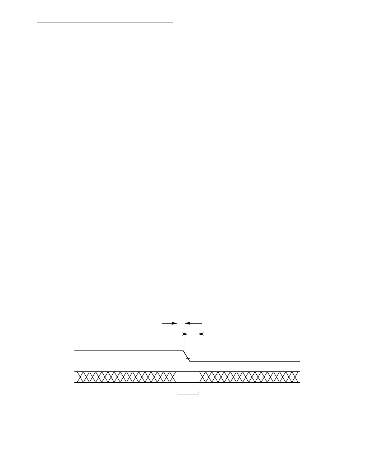
Bus Operation
aligned on word or long-word boundaries, respectively. The QUICC IDMAs, when used,
reduce the misalignment overhead to a minimum.
4.1 BUS TRANSFER SIGNALS
The bus transfers information between the QUICC and external memory or a peripheral
device. External devices can accept or provide 8, 16, or 32 bits in parallel and must follow
the handshake protocol described in this section. The maximum number of bits accepted or
provided during a bus transfer is defined as the port width. The QUICC contains an address
bus that specifies the address for the transfer and a data bus that transfers the data. Control
signals indicate the beginning and type of the cycle as well as the address space and size
of the transfer. The selected device then controls the length of the cycle with the signal(s)
used to terminate the cycle. Strobe signals, one for the address bus and another for the data
bus, indicate the validity of the address and provide timing information for the data.
Both asynchronous and synchronous operation is possible for any port width. In asynchronous operation, the bus and control input signals are internally synchronized to the QUICC
clock, introducing a delay. This delay is the time required for the QUICC to sample an input
signal, synchronize the input to the internal clocks, and determine whether it is high or low.
In synchronous mode, the bus and control input signals must be timed to setup and hold
times. Since no synchronization is needed, bus cycles can be completed in three clock
cycles in this mode. Additionally, using the fast-termination option of the chip-select signals,
two-clock operation is possible.
Furthermore, for all inputs, the QUICC latches the level of the input during a sample window
around the falling edge of the clock signal. This window is illustrated in Figure 4-1, where t
and t
are the input setup and hold times, respectively. To ensure that an input signal is rec-
h
su
ognized on a specific falling edge of the clock, that input must be stable during the sample
window. If an input makes a transition during the window time period, the level recognized
by the QUICC is not predictable; however, the QUICC always resolves the latched level to
either a logic high or low before using it. In addition to meeting input setup and hold times
for deterministic operation, all input signals must obey the protocols described in this section.
t
su
t
h
CLK
EXT
4-2
SAMPLE WINDOW
Figure 4-1. Input Sample Window
MC68360 USER’S MANUAL
MOTOROLA
Page 79

Bus Operation
4.1.1 Bus Control Signals
The QUICC initiates a bus cycle by driving the address, size, function code, and read/write
outputs. At the beginning of a bus cycle, SIZ1 and SIZ0 are driven with the FC signals. SIZ1
and SIZ0 indicate the number of bytes remaining to be transferred during an operand cycle
(consisting of one or more bus cycles). Table 4-3 lists the encoding of SIZ1 and SIZ0. These
signals are valid while AS
is asserted.
The R/W
beginning of a bus cycle, R/W
signal determines the direction of the transfer during a bus cycle. Driven at the
is valid while AS is asserted. R/W only transitions when a write
cycle is preceded by a read cycle or vice versa. The signal may remain low for consecutive
write cycles.
The RMC
signal is asserted at the beginning of the first bus cycle of a read-modify-write
operation and remains asserted until completion of the final bus cycle of the operation.
4.1.2 Function Codes (FC3–FC0)
The FCx signals are outputs that indicate one of 16 address spaces to which the address
applies. Fifteen of these spaces are designated as either a normal or DMA cycle, user or
supervisor, and program or data spaces. One other address space is designated as CPU
space to allow the CPU32+ to acquire specific control information not normally associated
with read or write bus cycles. The FCx signals are valid while AS
Function codes (see Table 4-1) can be considered as extensions of the 32-bit address that
can provide up to eight different 4-Gbyte address spaces. Function codes are automatically
generated by the CPU32+ to select address spaces for data and program at both user and
supervisor privilege levels, and a CPU address space for processor functions. User programs access only their own program and data areas to increase protection of system integrity and can be restricted from accessing other information. The S-bit in the CPU32+ status
register is set for supervisor accesses and cleared for user accesses to provide differentiation. Refer to 4.4 CPU Space Cycles for more information.
is asserted.
MOTOROLA
Table 4-1. Address Space Encoding
Function Code Bits
3210 Address Spaces
0000Reserved (Motorola)
0001User Data Space
0010User Program Space
0011Reserved (User)
0100Reserved (Motorola)
0101Supervisor Data Space
0110Supervisor Program Space
0111Supervisor CPU Space
1 x x x DMA space
MC68360 USER’S MANUAL
4-3
Page 80

Bus Operation
4.1.3 Address Bus (A31–A0)
The address bus signals are outputs that define the address of the byte (or the most significant byte) to be transferred during a bus cycle. The QUICC places the address on the bus
at the beginning of a bus cycle. The address is valid while AS
is asserted.
4.1.4 Address Strobe (AS)
AS is an output timing signal that indicates the validity of an address on the address bus and
of many control signals. AS
ning of a bus cycle.
is asserted approximately one-half clock cycle after the begin-
4.1.5 Data Bus (D31-D0)
The data bus is a bidirectional, nonmultiplexed, parallel bus that contains the data being
transferred to or from the QUICC. A read or write operation may transfer 8, 16, 24, or 32 bits
of data (one, two, three, or four bytes) in one bus cycle. During a read cycle, the data is
latched by the QUICC on the last falling edge of the clock for that bus cycle. For a write cycle,
all 32 bits of the data bus are driven, regardless of the port width or operand size. The
QUICC places the data on the data bus approximately one-half clock cycle after AS
asserted in a write cycle.
is
4.1.6 Data Strobe (DS)
DS is an output timing signal that applies to the data bus. For a read cycle, the QUICC
asserts DS
For a write cycle, DS
QUICC asserts DS
cycle.
and AS simultaneously to signal the external device to place data on the bus.
signals to the external device that the data to be written is valid. The
approximately one clock cycle after the assertion of AS during a write
4.1.7 Output Enable (OE)
OE is an output timing signal that applies to the data bus. On a read cycle, the QUICC
asserts OE
cycles with timing similar to AS
is not shown in the diagrams in this section. Use AS timing instead during read cycles.
OE
to signal the external device to place data on the bus. OE is asserted during read
.
4.1.8 Byte Write Enable (WE0, WE1, WE2, WE3)
The upper upper write enable (WE0) indicates that the upper eight bits of the data bus (D31–
D24) contain valid data during a write cycle. The upper middle write enable (WE1
that the upper middle eight bits of the data bus (D23–D16) contain valid data during a write
cycle. The lower middle write enable (WE2
data bus (D15–D8) contain valid data during a write cycle. The lower write enable (WE3
indicates that the lower eight bits of the data bus contain valid data during a write cycle.
) indicates that the lower middle eight bits of the
) indicates
)
4-4
MC68360 USER’S MANUAL
MOTOROLA
Page 81

Bus Operation
The equations of the byte write enables for 32-bit port (16BM = 1) are as follows:
WE0
= R/W + AS + A0 + A1
WE1 = R/W + AS + not {(A1 * SIZ0) + (A0 * A1) + (A1 * SIZ1)}
WE2 = R/W + AS + not {(A0 * A1) + (A1 * SIZ0 * SIZ1) + (A1 * SIZ0 * SIZ1) +
(A0 * A1 * SIZ0)}
WE3 = R/W + AS + not {(A0 * SIZ0 * SIZ1) + (SIZ0 * SIZ1) + (A0 * A1) + (A1 *
SIZ1)}
These signals have the same timing as AS. The equations are valid only for a 32-bit port.
The equations of the byte write enables for 16-bit port (B16M = 0) are as follows:
WE0
= R/W + AS + A0
WE1 = R/W + AS + (A0 * SIZ0 * SIZ1)
These signals have the same timing as AS. The equations are valid only for a 16-bit port.
signals are not shown in the diagrams in this section. Use AS timing instead during
WEx
write cycles. The particular WEx
signals that are active in a given bus cycle depend on which
bytes are being written.
NOTE
Note that the WE signals are not affected by dynamic bus sizing.
External assertion of DSACKx
will have no effect on which WEx
signal gets asserted.
When 16-bit mode is selected and Bit 7 of PEPAR is set, WE2
and WE3 are used as address lines A29 and A28 respectively.
4.1.9 Bus Cycle Termination Signals
The following signals can terminate a bus cycle.
4.1.9.1 DATA TRANSFER AND SIZE ACKNOWLEDGE (DSACK1 AND DSACK0). Dur-
ing bus cycles, external devices assert DSACK1
During a read cycle, this signals the QUICC to terminate the bus cycle and to latch the data.
During a write cycle, this indicates that the external device has successfully stored the data
and that the cycle may terminate. These signals also indicate to the QUICC the size of the
port for the bus cycle just completed (see Table 4-3). Refer to 4.3.1 Read Cycle for timing
relationships of DSACK1
and DSACK0.
Additionally, the system integration module (SIM60) can be programmed to internally generate DSACK1
and DSACK0 for external accesses, eliminating logic required to generate
these signals. The SIM60 can alternatively be programmed to generate a fast termination,
providing a two-cycle external access. Refer to 4.2.6 Fast Termination Cycles
information on these cycles.
and/or DSACK0 as part of the bus protocol.
for additional
4.1.9.2 BUS ERROR (BERR). This signal is also a bus cycle termination indicator and can
be used in the absence of DSACKx
asserted in conjunction with DSACKx
MOTOROLA
to indicate a bus error condition. BERR can also be
to indicate a bus error condition, provided it meets the
MC68360 USER’S MANUAL
4-5
Page 82

Bus Operation
appropriate timing described in this section and in Section 10 Electrical Characteristics.
Additionally, BERR
and HALT can be asserted together to indicate a retry termination. Refer
to 4.5 Bus Exception Control Cycles for additional information on the use of these signals.
See the memory controller description in Section 6 System Integration Module (SIM60) for
precautions about asserting BERR
externally too early during DRAM and SRAM cycles con-
trolled by the memory controller.
The internal bus monitor can be used to generate the BERR
signal for internal and external
transfers in all the following descriptions.
4.1.9.3 AUTOVECTOR (AVEC). This signal can be used to terminate interrupt acknowl-
edge cycles, indicating that the QUICC should internally generate a vector (autovector)
number to locate an interrupt handler routine. AVEC
can be generated either externally or
internally by the SIM60 (refer to Section 6 System Integration Module (SIM60) for additional
information). AVEC
is ignored during all other bus cycles.
4.2 DATA TRANSFER MECHANISM
The QUICC supports byte, word, and long-word operands, allowing access to 8-,16-, and
32-bit data ports through the use of asynchronous cycles controlled by DSACK1
DSACK0
. The QUICC also supports byte, word, and long-word operands, allowing access
and
to 8-, 16, and 32-bit data ports through the use of synchronous cycles controlled by the fasttermination capability of the SIM60.
4.2.1 Dynamic Bus Sizing
The QUICC dynamically interprets the port size of the addressed device during each bus
cycle, allowing operand transfers to or from 8-, 16-, and 32-bit ports. During an operand
transfer cycle, the slave device signals its port size (byte, word, or long word) and indicates
completion of the bus cycle to the QUICC through the use of the DSACKx
Table 4-2 for DSACKx
encoding.
inputs. Refer to
Table 4-2. DSACKx Encoding
DSACK1 DSACK0 Result
1 1 Insert Wait States in Current Bus Cycle
1 0 Complete Cycle—Data Bus Port Size is 8 Bits
0 1 Complete Cycle—Data Bus Port Size is 16 Bits
0 0 Complete Cycle—Data Bus Port Size is 32 Bits
For example, if the QUICC is executing an instruction that reads a long-word operand from
a long-word aligned address, it attempts to read 32 bits during the first bus cycle. (Refer to
4.2.2 Misaligned Operands for the case of a word or byte address.) If the port responds that
it is 32 bits wide, the QUICC latches all 32 bits of data and continues with the next operation.
If the port responds that it is 16 bits wide, the QUICC latches the 16 bits of valid data and
runs another bus cycle to obtain the other 16 bits. The operation for an 8-bit port is similar,
but requires four read cycles. The addressed device uses the DSACKx
4-6
MC68360 USER’S MANUAL
signals to indicate
MOTOROLA
Page 83

Bus Operation
the port width. For instance, a 32-bit device always returns DSACKx for a 32-bit port (regardless of whether the bus cycle is a byte, word, or long-word operation).
Dynamic bus sizing requires that the portion of the data bus used for a transfer to or from a
particular port size be fixed. A 32-bit port must reside on data bus bits 0–31, a 16-bit port
must reside on data bus bits 16–32, and an 8-bit port must reside on data bus bits 24–31.
This requirement minimizes the number of bus cycles needed to transfer data to 8- and 16bit ports and ensures that the QUICC correctly transfers valid data. The QUICC always
attempts to transfer the maximum amount of data on all bus cycles; for a long-word operation, it always assumes that the port is 32 bit wide when beginning the bus cycle.
The bytes of operands are designated as shown in Figure 4-2. The most significant byte of
a long-word operand is OP0, and OP3 is the least significant byte. The two bytes of a wordlength operand are OP2 (most significant) and OP3. The single byte of a byte-length operand is OP3. These designations are used in the figures and descriptions that follow.
31 0
LONG-WORD OPERAND
0P0 0P1 0P2 0P3
15 0
WORD OPERAND
0P2 0P3
70
BYTE OPERAND
0P3
Figure 4-2. Internal Operand Representation
Figure 4-3 shows the required organization of data ports on the QUICC bus for 8, 16, and
32-bit devices. The four bytes shown are connected through the internal data bus and data
multiplexer to the external data bus. This path is the means through which the QUICC supports dynamic bus sizing and operand misalignment. Refer to 4.2.2 Misaligned Operands
for the definition of misaligned operand. The data multiplexer establishes the necessary
connections for different combinations of address and data sizes.
The multiplexer takes the four bytes of the 32-bit bus and routes them to their required positions. For example, OP0 can be routed to D24–D31, as would be the normal case, or it can
be routed to any other byte position to support a misaligned transfer. The same is true for
any of the operand bytes. The positioning of bytes is determined by the size and address
outputs.
MOTOROLA
MC68360 USER’S MANUAL
4-7
Page 84

Bus Operation
0P0 0P1 0P2 0P3
INCREASING
MEMORY
ADDRESSES
REGISTER
MULTIPLEXER
EXTERNAL
DATA BUS
ADDRESS
xxxxxxxx0
xxxxxxxx0
xxxxxxxx0
0123
ROUTING AND DUPLICATION
INTERNAL TO
D31–D24
BYTE 0 BYTE 1 BYTE 2 BYTE 3
BYTE 0
2
1
2
3
BYTE 2
BYTE 0
BYTE 1
BYTE 2
BYTE 3
D23–D16
BYTE 1
BYTE 3
8-BIT PORT
D15–D8
16-BIT PORT
D7–D0
THE MC68360
EXTERNAL BUS
32-BIT PORT
Figure 4-3. QUICC Interface to Various Port Sizes
The SIZ0 and SIZ1 outputs indicate the remaining number of bytes to be transferred during
the current bus cycle (see Table 4-3).
Table 4-3. SIZx Encoding
SIZ1 SIZ0 Size
0 1 Byte
1 0 Word
1 1 3 Bytes
0 0 Long Word
The number of bytes transferred during a write or read bus cycle is equal to or less than the
size indicated by the SIZx outputs, depending on port width and operand alignment. For
example, during the first bus cycle of a long-word transfer to a word port, the SIZx outputs
indicate that four bytes are to be transferred, although only two bytes are moved on that bus
cycle.
A0 and A1 also affect operation of the data multiplexer. During an operand transfer, A2-A31
indicate the long-word base address of that portion of the operand to be accessed; A0 and
A1 indicate the byte offset from the base. Table 4-4 lists the encoding of A0 and A1 and the
corresponding byte offset from the long-word base.
4-8
MC68360 USER’S MANUAL
MOTOROLA
Page 85

Bus Operation
Table 4-4. Address Offset Encoding
A1 A0 Offset
0 0 +0 Byte
0 1 +1 Byte
1 0 +2 Bytes
1 1 +3 Bytes
Table 4-5 lists the bytes required on the data bus for read cycles. The entries shown as OPx
are portions of the requested operand that are read during that bus cycle and are defined
by SIZ0, SIZ1, A0, and A1 for the bus cycle. Bytes labeled x are “don’t cares” and are not
required during that read cycle.
Table 4-5. Data Bus Requirements for Read Cycles
Transfer
Size Size Address
SIZ1 SIZ0 A1 A0 D31:D24 D23:D16 D15:D8 D7:D0 D31:D24 D23:D16 D31:D24
Byte 0 1 0 0 OP3 x x x OP3 x OP3
0 1 0 1 x OP3 x x x OP3 OP3
0 1 1 0 x x OP3 x OP3 x OP3
0 1 1 1 x x x OP3 x OP3 OP3
Word 1 0 0 0 OP2 OP3 x x OP2 OP3 OP2
1 0 0 1 x OP2 OP3 x x OP2 OP2
1 0 1 0 x x OP2 OP3 OP2 OP3 OP2
1 0 1 1 x x x OP2 x OP2 OP2
3 Bytes 1 1 0 0 OP1 OP2 OP3 x OP1 OP2 OP1
1 1 0 1 x OP1 OP2 OP3 x OP1 OP1
1 1 1 0 x x OP1 OP2 OP1 OP2 OP1
1 1 1 1 x x x OP1 x OP1 OP1
Long
Word
0 0 0 0 OP0 OP1 OP2 OP3 OP0 OP1 OP0
0 0 0 1 x OP0 OP1 OP2 x OP0 OP0
0 0 1 0 x x OP0 OP1 OP0 OP1 OP0
0 0 1 1 x x x OP0 x OP0 OP0
Long-Word Port
External Data Bytes Required
Word Port External
Data Bytes Required
Byte Port
External Data
Bytes Required
Table 4-6 lists the combinations of SIZ0, SIZ1, A0, and A1 and the corresponding pattern of
the data transfer for write cycles from the internal multiplexer of the QUICC to the external
data bus. Bytes labeled x are “don't care.”
Figure 4-4 shows the transfer of a long-word operand to a word port. In the first bus cycle,
the QUICC places the four operand bytes on the external bus. Since the address is longword aligned in this example, the multiplexer follows the pattern in the entry of Table 4-6 corresponding to SIZ0, SIZ1, A0, A1 = 0000. The port latches the data on bits D16–D31 of the
data bus, asserts DSACK1
(DSACK0 remains negated), and the QUICC terminates the bus
cycle. It then starts a new bus cycle with SIZ0, SIZ1, A0, A1 = 1010 to transfer the remaining
MOTOROLA
MC68360 USER’S MANUAL
4-9
Page 86

Bus Operation
16 bits. SIZ0 and SIZ1 indicate that a word remains to be transferred; A0 and A1 indicate
that the word corresponds to an offset of two from the base address. The multiplexer follows
the pattern corresponding to this configuration of the size and address signals and places
the two least significant bytes of the long word on the word portion of the bus (D16–D31).
The bus cycle transfers the remaining bytes to the word-size port. Figure 4-5 shows the timing of the bus transfer signals for this operation.
Table 4-6. QUICC Internal to External Data Bus Multiplexer—Write Cycle
Transfer Size Size Address External Data Bus Connection
SIZ1 SIZ0 A1 A0 D31:D24 D23:D16 D15:D8 D7:D0
Byte 0100OP3 x x x
0101OP3OP3 x x
0110OP3 x OP3 x
0111OP3OP3 x OP3
Word 1000OP2OP3 x x
1001OP2OP2OP3 x
1010OP2OP3OP2OP3
1011OP2OP2 x OP2
3 Bytes 1100OP1OP2OP3 x
1101OP1OP1OP2OP3
1110OP1OP2OP1OP2
1111OP1 x OP2OP1
Long Word 0000OP0OP1OP2OP3
0001OP0OP0OP1OP2
0010OP0OP1OP0OP1
0011OP0OP0 x OP0
31 0
0P0 0P1 0P2 0P3
DATA BUSD31 D16
WORD MEMORY
MSB LSB
0P0 0P1
0P2 0P3
LONG-WORD OPERAND
SIZ1 SIZ0
0000
1010
MC68360
A1 A0
MEMORY CONTROL
DSACK1 DSACK0
LH
LH
Figure 4-4. Example of Long-Word Transfer to Word Port
4-10
MC68360 USER’S MANUAL
MOTOROLA
Page 87

S0 S2 S4 S0 S2 S4
CLKO1
A31–A2
FC3–FC0
SIZ1
SIZ0
R/W
A0
AS
A1
Bus Operation
DS
DSACK1
DSACK0
D31–D24
D23–D16
0P0
0P1
WORD WRITE
LONG-WORD OPERAND WRITE TO 16-BIT PORT
WORD WRITE
0P2
0P3
Figure 4-5. Long-Word Operand Write Timing (16-Bit Data Port)
Figure 4-6 shows a word transfer to an 8-bit bus port. Like the preceding example, this
example requires two bus cycles. Each bus cycle transfers a single byte. The size signals
for the first cycle specify two bytes; for the second cycle, they specify one byte. Figure 4-7
shows the associated bus transfer signal timing.
4.2.2 Misaligned Operands
Since operands may reside at any byte boundaries, they may be misaligned. A byte operand
is properly aligned at any address; a word operand is misaligned at an odd address; a long
word is misaligned at an address that is not evenly divisible by four. The MC68302,
MC68000/MC68008, MC68010, and MC68340 implementations allow long-word transfers
on odd-word boundaries but force exceptions if word or long-word operand transfers are
attempted at odd-byte addresses. Although the QUICC does not enforce any alignment
restrictions for data operands (including PC relative data addresses), some performance
degradation occurs when additional bus cycles are required for long-word or word operands
MOTOROLA
MC68360 USER’S MANUAL
4-11
Page 88
WORD OPERAND
15 0
Bus Operation
that are misaligned. For maximum performance, data items should be aligned on their natural boundaries. All instruction words and extension words must reside on word boundaries.
Attempting to prefetch an instruction word at an odd address causes an address error
exception.
0P2 0P3
DATA BUSD31 D24
BYTE MEMORY
0P2
0P3
SIZ1 SIZ0 A1
1000
0101
MC68360
A0
MEMORY CONTROL
DSACK1 DSACK0
Figure 4-6. Example of Word Transfer to Byte Port
LH
LH
4-12
MC68360 USER’S MANUAL
MOTOROLA
Page 89

CLKO1
A31–A2
A0
FC3–FC0
SIZ1
SIZ0
R/W
AS
A1
S0 S2 S4 S0 S2 S4
Bus Operation
DS
DSACK1
DSACK0
D31–D24
D23–D16
D15–D8
D7–D0
BYTE WRITE
OP2
OP3
OP2
OP3
WORD OPERAND WRITE
OP3
OP3
OP3
OP3
BYTE WRITE
Figure 4-7. Word Operand Write Timing (8-Bit Data Port)
Figure 4-8 shows the transfer of a long-word operand to an odd address in word-organized
memory, which requires three bus cycles. For the first cycle, the SIZx signals specify a longword transfer, and the address offset (A2–A0) is 001. Since the port width is 16 bits, only the
first byte of the long word is transferred. The slave device latches the byte and acknowledges the data transfer, indicating that the port is 16 bits wide. When the processor starts
the second cycle, the SIZx signals specify that three bytes remain to be transferred with an
address offset (A2–A0) of 010. The next two bytes are transferred during this cycle. The processor then initiates the third cycle, with the SIZx signals indicating one byte remaining to
be transferred. The address offset (A2–A0) is now 100; the port latches the final byte, and
the operation is complete. Figure 4-9 shows the associated bus transfer signal timing.
MOTOROLA
MC68360 USER’S MANUAL
4-13
Page 90

Bus Operation
31 0
0P0 0P1 0P2 0P3
D31 D16
DATA BUS
WORD MEMORY
MSB
XXX
0P1 0P2
LONG-WORD OPERAND
MC68360
LSB
0P0
XXXOP3 LH
SIZ1 SIZ0 A2 A1
0000
1101
01100
A0
MEMORY CONTROL
DSACK1 DSACK0
1
0
L
L
H
H
Figure 4-8. Misaligned Long-Word Transfer to Word Port Example
4-14
MC68360 USER’S MANUAL
MOTOROLA
Page 91

Bus Operation
S0 S2 S4 S0 S2 S4
CLKO1
A31–A2
A1
A0
FC3–FC0
SIZ1
SIZ0
R/W
AS
DS
DSACK1
S0 S2 S4
DSACK0
D31–D24
D23–D16
D15–D8
D7–D0
BYTE WRITE
0P0
0P0
0P1
0P2
WORD WRITE
LONG-WORD OPERAND WRITE
0P1
0P2
0P1
0P2
0P3
0P3
0P3
0P3
BYTE WRITE
Figure 4-9. Misaligned Long-Word Transfer to Word Port Timing
Figure 4-10 and Figure 4-11 show a word transfer to an odd address in word-organized
memory. This example is similar to the one shown in Figure 4-8 and Figure 4-9 except that
the operand is word sized and the transfer requires only two bus cycles.
MOTOROLA
MC68360 USER’S MANUAL
4-15
Page 92

Bus Operation
15
OP2 OP3
WORD MEMORY
MSB LSB
XXX
0P3
DATA BUSD31 D16
0P2
XXX
0WORD OPERAND
SIZ1 SIZ0 A2 A1
1 0 0 0 1
0 1 0 1 0
MC68360
A0
MEMORY CONTROL
DSACK1 DSACK0
LH
LH
Figure 4-10. Misaligned Word Transfer to Word Port Example
4-16
MC68360 USER’S MANUAL
MOTOROLA
Page 93

S0 S2 S4 S0
S4
CLKO1
A31–A2
A1
A0
FC3–FC0
SIZ1
SIZ0
R/W
S2
Bus Operation
AS
DS
DSACK1
DSACK0
D31–D24
D23–D16
D15–D8
D7–D0
0P2
0P2
0P3
0P2
WORD WRITE
WORD OPERAND WRITE TO A1/A0 = 01
0P3
0P3
0P3
0P3
BYTE WRITE
Figure 4-11. Misaligned Word Transfer to Word Port Timing
Figure 4-12 and Figure 4-13 show an example of a long-word transfer to an odd address in
long-word-organized memory. In this example, a long-word access is attempted beginning
at the least significant byte of a long-word-organized memory. Only one byte can be transferred in the first bus cycle. The second bus cycle then consists of a three-byte access to a
long-word boundary. Since the memory is long-word organized, no further bus cycles are
necessary.
MOTOROLA
MC68360 USER’S MANUAL
4-17
Page 94

Bus Operation
15
0P0
D31 D0
MSB UMB
XXX
0P1 0P2
LONG-WORD OPERAND
0P1
DATA BUS
LONG-WORD MEMORY
XXX
0P2 0P3
LMB LSB
0P0
0P3
0P0
XXX
0
MC68EC030
SIZ1 SIZ0 A2 A1
0 0 0 1 1
1 1 1 0 0
A0
Figure 4-12. Misaligned Long-Word Transfer to Long-Word Port Example
MEMORY CONTROL
DSACK1 DSACK0
L
LL
L
4-18
MC68360 USER’S MANUAL
MOTOROLA
Page 95

S0 S2 S4 S0 S2 S4
CLKO1
A31–A2
A0
FC2–FC0
SIZ1
SIZ0
R/W
A1
Bus Operation
AS
DS
DSACK1
DSACK0
D31–D24
D23–D16
D15–D8
D7–D0
0P0
0P0
0P1
0P0
BYTE WRITE
LONG-WORD OPERAND WRITE
0P1
0P2
0P3
0P1
3-BYTE WRITE
Figure 4-13. Misaligned Long-Word Transfer to Long-Word Port Timing
4.2.3 Effects of Dynamic Bus Sizing and Operand Misalignment
The combination of operand size, operand alignment, and port size determines the number
of bus cycles required to perform a particular memory access. Table 4-7 lists the number of
bus cycles required for different operand sizes to different port sizes with all possible alignment conditions for write cycles and read cycles.
MOTOROLA
MC68360 USER’S MANUAL
4-19
Page 96

Bus Operation
Table 4-7. Memory Alignment and Port Size Influence
on Write Bus Cycles
Number of Bus Cycles
A1–A0 00 01 10 11
Instruction
Byte Operand 1:1:1 1:1:1 1:1:1 1:1:1
Word Operand 1:1:2 1:2:2 1:1:2 2:2:2
Long-Word Operand 1:2:4 2:3:4 2:2:4 2:3:4
Notes:
1. Data Port Size—32 Bits:16 Bits:8 Bits
2. Instruction reads can either be two words from an
even-word boundary, or one word from an odd-word boundary.
1
1:2:4 N/A N/A N/A
This table verifies that bus cycle throughput is significantly affected by port size and alignment. The QUICC system designer and programmer should be aware of and account for
these effects, particularly in time-critical applications.
If the required instruction begins at an even-word boundary, the processor prefetches a long
word (up to two instructions) by reading a long word from a long-word address (A1–A0 = 00),
regardless of port size. When the required instruction begins at an odd-word boundary, the
processor reads 16-bits only, from the odd-word boundary. Refer to Section 5 CPU32+ for
a complete description of the pipeline operation.
4.2.4 Bus Operation
The QUICC bus is asynchronous, allowing external devices connected to the bus to operate
at clock frequencies different from the clock for the QUICC. Bus operation uses the handshake lines (AS
signals a valid address on the address bus, and DS is used as a condition for valid data on
a write cycle. Decoding the SIZx outputs and lower address lines (A1–A0) provides strobes
that select the active portion of the data bus. The slave device (memory or peripheral)
responds by placing the requested data on the correct portion of the data bus for a read
cycle or by latching the data on a write cycle; the slave asserts the DSACK1
bination that corresponds to the port size to terminate the cycle.
Alternatively, the SIM60 can be programmed to assert the DSACK1
internally and respond for the slave. If no slave responds or the access is invalid, external
control logic may assert BERR
tively. DSACKx
The length of time that DSACKx
asynchronous system to ensure that valid data is latched into the QUICC. (See Section 10
Electrical Characteristics for timing parameters.)
, DS, DSACK1, DSACK0, BERR, and HALT) to control data transfers. AS
/DSACK0 com-
/DSACK0 combination
or BERR with HALT to abort or retry the bus cycle, respec-
can be asserted before the data from a slave device is valid on a read cycle.
may precede data must not exceed a specified value in any
Note that no maximum time is specified from the assertion of AS
DSACKx
the cycle is terminated with DSACKx
ments until DSACKx
asserted. BERR
4-20
. Although the QUICC can transfer data in a minimum of three clock cycles when
, the QUICC inserts wait cycles in clock-period incre-
is recognized. BERR and/or HALT can be asserted after DSACKx is
and/or HALT must be asserted within the time specified after DSACKx is
MC68360 USER’S MANUAL
to the assertion of
MOTOROLA
Page 97

Bus Operation
asserted in any asynchronous system. If this maximum delay time is violated, the QUICC
may exhibit erratic behavior.
4.2.5 Synchronous Operation with DSACKx
Although cycles terminated with DSACKx are classified as asynchronous, cycles terminated
with DSACKx
edges. The devices that use these cycles must synchronize the response to the QUICC
clock (CLKO1) to be synchronous. Since the devices terminate bus cycles with DSACKx
the dynamic bus sizing capabilities of the QUICC are available. The minimum cycle time for
these cycles is also three clocks. To support systems that use the system clock to generate
DSACKx
chronous input hold time are given. If the setup and hold times are met for the assertion or
negation of a signal, such as DSACKx
level on that specific falling edge of the system clock. If the assertion of DSACKx
nized on a particular falling edge of the clock, valid data is latched into the QUICC (for a read
cycle) on the next falling clock edge if the data meets the data setup time. In this case, the
parameter for asynchronous operation can be ignored. The timing parameters are described
in Section 10 Electrical Characteristics.
can also operate synchronously in that signals are interpreted relative to clock
and other asynchronous inputs, the asynchronous input setup time and the asyn-
, the QUICC is guaranteed to recognize that signal
is recog-
,
If a system asserts DSACKx
obeys the proper bus protocol by maintaining DSACKx
throughout the clock edge that negates AS
time), no wait states are inserted. The bus cycle runs at its maximum speed for bus cycles
terminated with DSACKx
asserted after DSACKx
the falling clock edge one clock cycle after DSACKx
and the QUICC may exhibit erratic behavior if it is violated. When operating synchronously,
the data-in setup and hold times for synchronous cycles may be used instead of the timing
requirements for data relative to DS
, BERR (and HALT) must meet the appropriate setup time prior to
for the required window around the falling edge of S2 and
(and/or BERR/HALT) until and
(with the appropriate asynchronous input hold
(three clocks per cycle). When BERR (or BERR and HALT) is
is recognized. This setup time is critical,
.
4.2.6 Fast Termination Cycles
With an external device that has a fast access time, the memory controller circuits can provide a two-clock external bus transfer. Since the memory controller circuits are driven from
the system clock, the bus cycle termination is inherently synchronized with the system clock.
Refer to Section 6 System Integration Module (SIM60) for more information on chip selects
and the DRAM controller. To use the fast termination (cycle length is two clocks) option, an
external device should be fast enough to have data ready, within the specified setup time,
by the falling edge of S4. Figure 4-14 shows the DSACKx
states, followed by a fast termination read and write.
timing for a read with two wait
MOTOROLA MC68360 USER’S MANUAL 4-21
Page 98
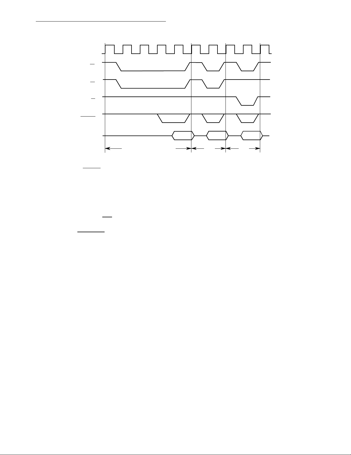
Bus Operation
*
*
CLKO1
AS
DS
R/W
DSACKx
D31–D0
S0 S2 SW SW S4 S0 S4 S0 S4 S0
S1 S3 S5 S1 S5 S1 S5SW
TWO WAIT STATES IN READ
SW
* DSACKx only internally asserted for fast termination cycles.
Figure 4-14. Fast Termination Timing
NOTES
FAST
TERMINATION
READ
FAST
TERMINATION
WRITE
When using the fast termination option (cycle length is two
clocks), DS
DSACKx
is asserted only in a read cycle, not in a write cycle.
is only internally asserted for fast termination cycles.
4.3 DATA TRANSFER CYCLES
The transfer of data between the QUICC and other devices involves the following signals:
• Address Bus A31–A0
• Data Bus D31–D0
• Control Signals
The address and data buses are both parallel, nonmultiplexed buses. The bus master
moves data on the bus by issuing control signals, and the bus uses a handshake protocol
to ensure correct movement of the data. In all bus cycles, the bus master is responsible for
deskewing all signals it issues at both the start and end of the cycle. In addition, the bus master is responsible for deskewing the acknowledge and data signals from the slave devices.
The following paragraphs define read, write, and read-modify-write cycle operations. Each
bus cycle is defined as a succession of states that apply to the bus operation. These states
are different from the QUICC states described for the CPU32+. The clock cycles used in the
descriptions and timing diagrams of data transfer cycles are independent of the clock frequency. Bus operations are described in terms of external bus states.
4-22 MC68360 USER’S MANUAL MOTOROLA
Page 99

Bus Operation
EXTERNAL DEVICE
4.3.1 Read Cycle
During a read cycle, the QUICC receives data from a memory or peripheral device. If the
instruction specifies a long-word operation, the QUICC attempts to read four bytes at once.
For a word operation, the QUICC attempts to read two bytes at once. For a byte operation,
the QUICC reads one byte. The section of the data bus from which each byte is read
depends on the operand size, address signals (A1, A0), and the port size. Refer to 4.2.1
Dynamic Bus Sizing and 4.2.2 Misaligned Operands for more information.
Figure 4-15 shows a long-word read cycle flowchart and Figure 4-16 illustrates a byte read
cycle flowchart. Figure 4-17 and Figure 4-18 show functional read cycles timing diagrams
specified in terms of clock periods.
BUS MASTER
ADDRESS DEVICE
1) SET R/W TO READ
2) DRIVE ADDRESS ON A31–A0
3) DRIVE FUNCTION CODE ON FC3–FC0
4) DRIVE SIZx PINS FOR FOUR BTYES
5) ASSERT AS, OE AND DS
ACQUIRE DATA
1) LATCH DATA
2) NEGATE AS, OE AND DS
START NEXT CYCLE
1) DECODE ADDRESS
2) PLACE DATA ON D31–D0
3) DRIVE DSACKx SIGNALS
1) REMOVE DATA FROM D31–D0
2) NEGATE DSACKx
SLAVE
PRESENT DATA
TERMINATE CYCLE
Figure 4-15. Long-Word Read Cycle Flowchart
BUS MASTER
ADDRESS DEVICE
1) SET R/W TO READ
2) DRIVE ADDRESS ON A31–A0
3) DRIVE FUNCTION CODE ON FC3–FC0
4) DRIVE SIZE (SIZ1–SIZ0) (ONE BYTE)
5) ASSERT AS, DS, AND OE
TERMINATE OUTPUT TRANSFER
1) DECODE ADDRESS
2) PLACE DATA ON D31–D24, OR D23–16, OR
D15–D8, OR D7–D0.
3) ASSERT DSACKx
PRESENT DATA
1) LATCH DATA
2) NEGATE AS, DS, AND OE
TERMINATE CYCLE
1) REMOVE DATA FROM D31–D0
START NEXT CYCLE
2) NEGATE DSACKx
Figure 4-16. Byte Read Cycle Flowchart
MOTOROLA MC68360 USER’S MANUAL 4-23
Page 100

Bus Operation
S0 S2 S4 S0
CLKO1
A31–A2
A1
A0
FC3–FC0
SIZ1
WORD
SIZ0
R/W
AS
OE
S2
BYTE
S4
S0 S2 S4
DSACK1
DSACK0
D31–D24
D23–D16
D15–D8
D7–D0
DS
0P2
0P3
0P3
WORD READ
BYTE READ
BYTE READ
Figure 4-17. Byte and Word Read Cycles—32-Bit Port Timing
0P3
4-24 MC68360 USER’S MANUAL MOTOROLA
 Loading...