


Microprocessors and Memory
Technologies Group
MC68302
Integrated Multiprotocol Processor
User’s Manual
Motorola reserves the right to make changes without further notice to any products herein. Motorola makes no warranty, representation or guarantee regarding
the suitability of its products for any particular purpose, nor does Motorola assume any liability arising out of the application or use of any product or circuit, and
specifically disclaims any and all liability, including without limitation consequential or incidental damages. "Typical" parameters can and do vary in different
applications. All operating parameters, including "T ypicals" must be validated for each customer application by customer's technical experts. Motorola does not
convey any license under its patent rights nor the rights of others. Motorola products are not designed, intended, or authorized for use as components in
systems intended for surgical implant into the body, or other applications intended to support or sustain life, or for any other application in which the failure of the
Motorola product could create a situation where personal injury or death may occur. Should Buyer purchase or use Motorola products for any such unintended
or unauthorized application, Buyer shall indemnify and hold Motorola and its officers, employees, subsidiaries, affiliates, and distributors harmless against all
claims, costs, damages, and expenses, and reasonable attorney fees arising out of, directly or indirectly, any claim of personal injury or death associated with
such unintended or unauthorized use, even if such claim alleges that Motorola was negligent regarding the design or manufacture of the part. Motorola and
are registered trademarks of Motorola, Inc. Motorola, Inc. is an Equal Opportunity/Affirmative Action Employer .
Literature Distribution Centers:
USA/EUROPE: Motorola Literature Distribution; P.O. Box 20912, Arizona 85036.
JAPAN: Nippon Motorola Ltd.; 4-32-1, Nishi-Gotanda, Shinagawa-ku, Tokyo 141 Japan.
ASIA-PACIFIC: Motorola Semiconductors H.K. Ltd.; Silicon Harbour Center, No. 2 Dai King Street, Tai Po Industrial Estate,
1995 Motorola, Inc. All Rights Reserved

ii
MC68302 USER’S MANUAL
MOTOROLA

PREFACE
The complete documentation package for the MC68302 consists of the M68000PM/AD,
MC68000 Family Programmer’s Reference Manual,
Multiprotocol Processor User’s Manual,
tocol Processor Product Brief
.
and the MC68302/D,
MC68302UM/AD,
MC68302 Integrated Multipro-
MC68302 Integrated
MC68302 Integrated Multiprotocol Processor User’s Manual
The
ming, capabilities, registers, and operation of the MC68302; the
mer’s Reference Manual
Low Power Integrated Multiprotocol Processor Product Brief
the MC68302 capabilities.
This user’s manual is organized as follows:
Section 1 General Description
Section 2 MC68000/MC68008 Core
Section 3 System Integration Block (SIB)
Section 4 Communications Processor (CP)
Section 5 Signal Description
Section 6 Electrical Characteristics
Section 7 Mechanical Data And Ordering Information
Appendix B Development Tools and Support
Appendix C RISC Microcode from RAM
Appendix D MC68302 Applications
Appendix E SCC Programming Reference
Appendix F Design Checklist
provides instruction details for the MC68302; and
provides a brief description of
describes the program-
MC68000 Family Program-
the
MC68302
ELECTRONIC SUPPORT:
The Technical Support BBS, known as AESOP (Application Engineering Support Through
On-Line Productivity), can be reach by modem or the internet. AESOP provides commonly
asked application questons, latest device errata, device specs, software code, and many
other useful support functions.
Modem: Call 1-800-843-3451 (outside US or Canada 512-891-3650) on a modem that runs
at 14,400 bps or slower. Set your software to N/8/1/F emulating a vt100.
Internet: This access is provided by telneting to pirs.aus.sps.mot.com [129.38.233.1] or
through the World Wide Web at http://pirs.aus.sps.mot.com.
—
Sales Offices —
For questions or comments pertaining to technical information, questions, and applications,
please contact one of the following sales offices nearest you.
MOTOROLA
MC68302 USER’S MANUAL
iii

iv
UNITED STATES
ALABAMA , Huntsville (205) 464-6800
ARIZONA , Tempe (602) 897-5056
CALIFORNIA , Agoura Hills (818) 706-1929
CALIFORNIA , Los Angeles (310) 417-8848
CALIFORNIA , Irvine (714) 753-7360
CALIFORNIA , Rosevllle (916) 922-7152
CALIFORNIA , San Diego (619) 541-2163
CALIFORNIA , Sunnyvale (408) 749-0510
COLORADO , Colorado Springs (719) 599-7497
COLORADO , Denver (303) 337-3434
CONNECTICUT , Wallingford (203) 949-4100
FLORIDA , Maitland (407) 628-2636
FLORIDA , Pompano Beach/
Fort Lauderdal (305) 486-9776
FLORIDA , Clearwater (813) 538-7750
GEORGlA , Atlanta (404) 729-7100
IDAHO , Boise (208) 323-9413
ILLINOIS , Chicago/Hoffman Estates (708) 490-9500
INDlANA , Fort Wayne (219) 436-5818
INDIANA , Indianapolis (317) 571-0400
INDIANA , Kokomo (317) 457-6634
IOWA , Cedar Rapids (319) 373-1328
KANSAS , Kansas City/Mission (913) 451-8555
MARYLAND , Columbia (410) 381-1570
BRITISH COLUMBIA , Vancouver (604) 293-7605
ONTARIO , Toronto (416) 497-8181
ONTARIO , Ottawa (613) 226-3491
QUEBEC , Montreal (514) 731-6881
AUSTRALIA , Melbourne (61-3)887-0711
AUSTRALIA , Sydney (61(2)906-3855
BRAZIL , Sao Paulo 55(11)815-4200
CHINA , Beijing 86 505-2180
FINLAND , Helsinki 358-0-35161191
Car Phone 358(49)211501
FRANCE , Paris/Vanves 33(1)40 955 900
GERMANY , Langenhagen/ Hanover 49(511)789911
GERMANY , Munich 49 89 92103-0
GERMANY , Nuremberg 49 911 64-3044
GERMANY , Sindelfingen 49 7031 69 910
GERMANY ,Wiesbaden 49 611 761921
HONG KONG , Kwai Fong 852-4808333
Tai Po 852-6668333
INDIA , Bangalore (91-812)627094
ISRAEL , Tel Aviv 972(3)753-8222
ITALY , Milan 39(2)82201
JAPAN , Aizu 81(241)272231
JAPAN , Atsugi 81(0462)23-0761
JAPAN , Kumagaya 81(0485)26-2600
JAPAN , Kyushu 81(092)771-4212
JAPAN , Mito 81(0292)26-2340
JAPAN , Nagoya 81(052)232-1621
JAPAN , Osaka 81(06)305-1801
JAPAN, Sendai 81(22)268-4333
JAPAN,
JAPAN,
JAPAN
KOREA , Pusan 82(51)4635-035
KOREA , Seoul 82(2)554-5188
Tachikawa 81(0425)23-6700
Tokyo 81(03)3440-3311
, Yokohama 81(045)472-2751
CANADA
INTERNATIONAL
MASSACHUSETTS , Marborough (508) 481-8100
MASSACHUSETTS , Woburn (617) 932-9700
MICHIGAN , Detroit (313) 347-6800
MINNESOTA , Minnetonka (612) 932-1500
MISSOURI , St. Louis (314) 275-7380
NEW JERSEY , Fairfield (201) 808-2400
NEW YORK , Fairport (716) 425-4000
NEW YORK , Hauppauge (516) 361-7000
NEW YORK , Poughkeepsie/Fishkill (914) 473-8102
NORTH CAROLINA , Raleigh (919) 870-4355
OHIO , Cleveland (216) 349-3100
OHIO , Columbus Worthington (614) 431-8492
OHIO , Dayton (513) 495-6800
OKLAHOMA , Tulsa (800) 544-9496
OREGON , Portland (503) 641-3681
PENNSYLVANIA , Colmar (215) 997-1020
Philadelphia/Horsham (215) 957-4100
TENNESSEE , Knoxville (615) 690-5593
TEXAS , Austin (512) 873-2000
TEXAS , Houston (800) 343-2692
TEXAS , Plano (214) 516-5100
VIRGINIA , Richmond (804) 285-2100
WASHINGTON , Bellevue (206) 454-4160
Seattle Access (206) 622-9960
WISCONSIN , Milwaukee/Brookfield (414) 792-0122
MALAYSIA , Penang 60(4)374514
MEXICO , Mexico City 52(5)282-2864
MEXICO , Guadalajara 52(36)21-8977
Marketing 52(36)21-9023
Customer Service 52(36)669-9160
NETHERLANDS , Best (31)49988 612 11
PUERTO RICO , San Juan (809)793-2170
SINGAPORE
SPAIN , Madrid 34(1)457-8204
or 34(1)457-8254
SWEDEN , Solna 46(8)734-8800
SWITZERLAND , Geneva 41(22)7991111
SWITZERLAND , Zurich 41(1)730 4074
TAlWAN , Taipei 886(2)717-7089
THAILAND, Bangkok (66-2)254-4910
UNITED KINGDOM, Aylesbury 44(296)395-252
FULL LINE REPRESENTATIVES
COLORADO, Grand Junction
Cheryl Lee Whltely (303) 243-9658
KANSAS, Wichita
Melinda Shores/Kelly Greiving (316) 838 0190
NEVADA, Reno
Galena Technology Group (702) 746 0642
NEW MEXICO, Albuquerque
S&S Technologies, lnc. (505) 298-7177
UTAH, Salt Lake City
Utah Component Sales, Inc. (801) 561-5099
WASHINGTON, Spokane
Doug Kenley (509) 924-2322
ARGENTINA, Buenos Aires
Argonics, S.A. (541) 343-1787
HYBRID COMPONENTS RESELLERS
Elmo Semiconductor (818) 768-7400
Minco Technology Labs Inc. (512) 834-2022
Semi Dice Inc. (310) 594-4631
(65)2945438
MC68302 USER’S MANUAL
MOTOROLA

TABLE OF CONTENTS
Paragraph Title Page
Number Number
Section 1
General Description
1.1 Block Diagram......................................................................................... 1-1
1.2 Features.................................................................................................. 1-3
1.3 MC68302 System Architecture ............................................................... 1-4
1.4 NMSI Communications-Oriented Environment....................................... 1-5
1.5 Basic Rate ISDN or Digital Voice/Data Terminal .................................... 1-6
Section 2
MC68000/MC68008 Core
2.1 Programming Model................................................................................ 2-1
2.2 Instruction Set Summary......................................................................... 2-3
2.3 Address Spaces...................................................................................... 2-6
2.4 Exception Processing.............................................................................. 2-8
2.4.1 Exception Vectors................................................................................... 2-8
2.4.2 Exception Stacking Order .......................................................................2-9
2.5 Interrupt Processing.............................................................................. 2-11
2.6 M68000 Signal Differences................................................................... 2-11
2.7 MC68302 IMP Configuration Control.................................................... 2-12
2.8 MC68302 Memory Map......................................................................... 2-14
2.9 Event Registers..................................................................................... 2-19
Section 3
System Integration Block (SIB)
3.1 DMA Control............................................................................................ 3-2
3.1.1 Key Features........................................................................................... 3-2
3.1.2 IDMA Registers (Independent DMA Controller)...................................... 3-3
3.1.2.1 Channel Mode Register (CMR)............................................................... 3-4
3.1.2.2 Source Address Pointer Register (SAPR)............................................... 3-6
3.1.2.3 Destination Address Pointer Register (DAPR)........................................ 3-6
3.1.2.4 Function Code Register (FCR)................................................................ 3-7
3.1.2.5 Byte Count Register (BCR)..................................................................... 3-7
3.1.2.6 Channel Status Register (CSR).............................................................. 3-7
3.1.3 Interface Signals .....................................................................................3-8
3.1.3.1 DREQ
3.1.3.2 DONE
3.1.4 IDMA Operational Description................................................................. 3-9
3.1.4.1 Channel Initialization............................................................................... 3-9
3.1.4.2 Data Transfer.......................................................................................... 3-9
MOTOROLA
and DACK.................................................................................... 3-8
...................................................................................................... 3-8
MC68302 USER’S MANUAL
v

vi
Table of Contents
Paragraph Title Page
Number Number
3.1.4.3 Address Sequencing..............................................................................3-10
3.1.4.4 Transfer Request Generation ................................................................3-11
3.1.4.5 Block Transfer Termination....................................................................3-12
3.1.5 IDMA Programming ...............................................................................3-13
3.1.6 DMA Bus Arbitration ..............................................................................3-14
3.1.7 Bus Exceptions......................................................................................3-14
3.1.7.1 Reset......................................................................................................3-15
3.1.7.2 Bus Error................................................................................................3-15
3.1.7.3 Halt.........................................................................................................3-15
3.1.7.4 Relinquish and Retry..............................................................................3-15
3.2 Interrupt Controller.................................................................................3-15
3.2.1 Overview................................................................................................3-16
3.2.1.1 IMP Interrupt Processing Overview .......................................................3-16
3.2.1.2 Interrupt Controller Overview.................................................................3-17
3.2.2 Interrupt Priorities...................................................................................3-18
3.2.2.1 INRQ and EXRQ Priority Levels............................................................3-18
3.2.2.2 INRQ Interrupt Source Priorities............................................................3-19
3.2.2.3 Nested Interrupts ...................................................................................3-19
3.2.3 Masking Interrupt Sources and Events..................................................3-20
3.2.4 Interrupt Vector......................................................................................3-21
3.2.5 Interrupt Controller Programming Model................................................3-24
3.2.5.1 Global Interrupt Mode Register (GIMR).................................................3-24
3.2.5.2 Interrupt Pending Register (IPR)............................................................3-26
3.2.5.3 Interrupt Mask Register (IMR)................................................................3-27
3.2.5.4 Interrupt In-Service Register (ISR).........................................................3-28
3.2.6 Interrupt Handler Examples...................................................................3-28
3.3 Parallel I/O Ports....................................................................................3-29
3.3.1 Port A.....................................................................................................3-29
3.3.2 Port B.....................................................................................................3-31
3.3.2.1 PB7–PB0 ...............................................................................................3-31
3.3.2.2 PB11–PB8 .............................................................................................3-32
3.3.3 I/O Port Registers ..................................................................................3-32
3.4 Dual-Port RAM.......................................................................................3-33
3.5 Timers....................................................................................................3-35
3.5.1 Timer Key Features ...............................................................................3-36
3.5.2 General Purpose Timer Units ................................................................3-37
3.5.2.1 Timer Mode Register (TMR1, TMR2) ....................................................3-37
3.5.2.2 Timer Reference Registers (TRR1, TRR2)............................................3-38
3.5.2.3 Timer Capture Registers (TCR1, TCR2)................................................3-39
3.5.2.4 Timer Counter (TCN1, TCN2)................................................................3-39
3.5.2.5 Timer Event Registers (TER1, TER2)....................................................3-39
3.5.2.6 General Purpose Timer Example...........................................................3-40
3.5.2.6.1 Timer Example 1....................................................................................3-40
3.5.2.6.2 Timer Example 2....................................................................................3-40
3.5.3 Timer 3 - Software Watchdog Timer......................................................3-41
MC68302 USER’S MANUAL
MOTOROLA

Table of Contents
Paragraph Title Page
Number Number
3.5.3.1 Software Watchdog Timer Operation.................................................... 3-41
3.5.3.2 Software Watchdog Reference Register (WRR)................................... 3-41
3.5.3.3 Software Watchdog Counter (WCN).....................................................3-42
3.6 External Chip-Select Signals and Wait-State Logic.............................. 3-42
3.6.1 Chip-Select Logic Key Features............................................................ 3-45
3.6.2 Chip-Select Registers............................................................................3-45
3.6.2.1 Base Register (BR3–BR0) .................................................................... 3-45
3.6.2.2 Option Registers (OR3–OR0) ............................................................... 3-47
3.6.3 Chip Select Example............................................................................. 3-48
3.7 On-Chip Clock Generator...................................................................... 3-49
3.8 System Control...................................................................................... 3-50
3.8.1 System Control Register (SCR) ............................................................ 3-50
3.8.2 System Status Bits................................................................................3-51
3.8.3 System Control Bits............................................................................... 3-52
3.8.4 Disable CPU Logic (M68000)................................................................ 3-54
3.8.5 Bus Arbitration Logic.............................................................................3-56
3.8.5.1 Internal Bus Arbitration..........................................................................3-56
3.8.5.2 External Bus Arbitration......................................................................... 3-58
3.8.6 Hardware Watchdog..............................................................................3-59
3.8.7 Reducing Power Consumption.............................................................. 3-60
3.8.7.1 Power-Saving Tips................................................................................3-60
3.8.7.2 Low-Power (Standby) Modes................................................................ 3-60
3.8.7.2.1 Low-Power Mode .................................................................................. 3-61
3.8.7.2.2 Lowest Power Mode..............................................................................3-62
3.8.7.2.3 Lowest Power Mode with External Clock..............................................3-62
3.9 Clock Control Register.......................................................................... 3-64
3.9.1 Freeze Control.......................................................................................3-65
3.10 Dynamic Ram Refresh Controller.......................................................... 3-66
3.10.1 Hardware Setup .................................................................................... 3-66
3.10.2 DRAM Refresh Controller Bus Timing................................................... 3-67
3.10.3 Refresh Request Calculations...............................................................3-67
3.10.4 Initialization............................................................................................ 3-68
3.10.5 DRAM Refresh Memory Map................................................................3-68
3.10.6 Programming Example..........................................................................3-69
Section 4
Communications Processor (CP)
4.1 Main Controller........................................................................................4-1
4.2 SDMA Channels...................................................................................... 4-3
4.3 Command Set......................................................................................... 4-5
4.3.1 Command Execution Latency ................................................................. 4-7
4.4 Serial Channels Physical Interface..........................................................4-7
4.4.1 IDL Interface.......................................................................................... 4-11
4.4.2 GCI Interface......................................................................................... 4-14
4.4.3 PCM Highway Mode..............................................................................4-16
4.4.4 Nonmultiplexed Serial Interface (NMSI)................................................ 4-19
MOTOROLA
MC68302 USER’S MANUAL
vii

Table of Contents
Paragraph Title Page
Number Number
4.4.5 Serial Interface Registers.......................................................................4-19
4.4.5.1 Serial Interface Mode Register (SIMODE).............................................4-19
4.4.5.2 Serial Interface Mask Register (SIMASK)..............................................4-22
4.5 Serial Communication Controllers (SCCs).............................................4-22
4.5.1 SCC Features........................................................................................4-24
4.5.2 SCC Configuration Register (SCON).....................................................4-24
4.5.2.1 Asynchronous Baud Rate Generator Examples....................................4-26
4.5.2.2 Synchronous Baud Rate Generator Examples......................................4-27
4.5.3 SCC Mode Register (SCM)....................................................................4-27
4.5.4 SCC Data Synchronization Register (DSR)...........................................4-31
4.5.5 Buffer Descriptors Table........................................................................4-32
4.5.6 SCC Parameter RAM Memory Map.......................................................4-34
4.5.6.1 Data Buffer Function Code Register (TFCR, RFCR).............................4-35
4.5.6.2 Maximum Receive Buffer Length Register (MRBLR) ............................4-36
4.5.6.3 Receiver Buffer Descriptor Number (RBD#)..........................................4-36
4.5.6.4 Transmit Buffer Descriptor Number (TBD#)...........................................4-36
4.5.6.5 Other General Parameters.....................................................................4-37
4.5.7 SCC Initialization....................................................................................4-37
4.5.8 Interrupt Mechanism..............................................................................4-38
4.5.8.1 SCC Event Register (SCCE) .................................................................4-38
4.5.8.2 SCC Mask Register (SCCM) .................................................................4-39
4.5.8.3 SCC Status Register (SCCs).................................................................4-39
4.5.8.4 Bus Error on SDMA Access...................................................................4-40
4.5.9 SCC Transparent Mode.........................................................................4-41
4.5.10 Disabling the SCCs................................................................................4-42
4.5.11 UART Controller.....................................................................................4-43
4.5.11.1 Normal Asynchronous Mode..................................................................4-45
4.5.11.2 Asynchronous DDCMP MODE..............................................................4-46
4.5.11.3 UART Memory Map...............................................................................4-46
4.5.11.4 UART Programming Model....................................................................4-48
4.5.11.5 UART Command Set.............................................................................4-49
4.5.11.6 UART Address Recognition...................................................................4-50
4.5.11.7 UART Control Characters and Flow Control..........................................4-51
4.5.11.8 Send Break............................................................................................4-53
4.5.11.9 Send Preamble (IDLE)...........................................................................4-53
4.5.11.10 Wakeup Timer........................................................................................4-53
4.5.11.11 UART Error-Handling Procedure...........................................................4-54
4.5.11.12 Fractional Stop Bits................................................................................4-55
4.5.11.13 UART Mode Register.............................................................................4-56
4.5.11.14 UART Receive Buffer Descriptor (Rx BD) .............................................4-57
4.5.11.15 UART Transmit Buffer Descriptor (Tx BD).............................................4-61
4.5.11.16 UART Event Register.............................................................................4-63
4.5.11.17 UART MASK Register............................................................................4-65
4.5.11.18 S-Records Programming Example ........................................................4-65
4.5.12 HDLC Controller.....................................................................................4-66
viii
MC68302 USER’S MANUAL
MOTOROLA

Table of Contents
Paragraph Title Page
Number Number
4.5.12.1 HDLC Channel Frame Transmission Processing..................................4-68
4.5.12.2 HDLC Channel Frame Reception Processing....................................... 4-68
4.5.12.3 HDLC Memory Map...............................................................................4-69
4.5.12.4 HDLC Programming Model................................................................... 4-69
4.5.12.5 HDLC Command Set.............................................................................4-70
4.5.12.6 HDLC Address Recognition.................................................................. 4-71
4.5.12.7 HDLC Maximum Frame Length Register (MFLR).................................4-71
4.5.12.8 HDLC Error-Handling Procedure...........................................................4-72
4.5.12.9 HDLC Mode Register............................................................................ 4-73
4.5.12.10 HDLC Receive Buffer Descriptor (Rx BD).............................................4-75
4.5.12.11 HDLC Transmit Buffer Descriptor (Tx BD)............................................4-78
4.5.12.12 HDLC Event Register............................................................................ 4-80
4.5.12.13 HDLC Mask Register............................................................................. 4-82
4.5.13 BISYNC Controller ................................................................................ 4-82
4.5.13.1 Bisync Channel frame Transmission Processing..................................4-84
4.5.13.2 Bisync Channel Frame Reception Processing......................................4-85
4.5.13.3 Bisync Memory Map.............................................................................. 4-85
4.5.13.4 BISYNC Command Set.........................................................................4-86
4.5.13.5 BISYNC Control Character Recognition................................................4-87
4.5.13.6 BSYNC-BISYNC SYNC Register..........................................................4-89
4.5.13.7 BDLE-BISYNC DLE Register................................................................4-89
4.5.13.8 BISYNC Error-Handling Procedure.......................................................4-90
4.5.13.9 BISYNC Mode Register.........................................................................4-91
4.5.13.10 BISYNC Receive Buffer Descriptor (Rx BD).........................................4-93
4.5.13.11 BISYNC Transmit Buffer Descriptor (Tx BD)......................................... 4-95
4.5.13.12 BISYNC Event Register ........................................................................ 4-97
4.5.13.13 BISYNC Mask Register......................................................................... 4-98
4.5.13.14 Programming the BISYNC Controllers.................................................. 4-99
4.5.14 DDCMP Controller............................................................................... 4-100
4.5.14.1 DDCMP Channel Frame Transmission Processing............................ 4-101
4.5.14.2 DDCMP Channel Frame Reception Processing................................. 4-102
4.5.14.3 DDCMP Memory Map......................................................................... 4-103
4.5.14.4 DDCMP Programming Model.............................................................. 4-104
4.5.14.5 DDCMP Command Set....................................................................... 4-104
4.5.14.6 DDCMP Control Character Recognition.............................................. 4-105
4.5.14.7 DDCMP Address Recognition.............................................................4-106
4.5.14.8 DDCMP Error-Handling Procedure..................................................... 4-106
4.5.14.9 DDCMP Mode Register....................................................................... 4-108
4.5.14.10 DDCMP Receive Buffer Descriptor (Rx BD) ....................................... 4-109
4.5.14.11 DDCMP Transmit Buffer Descriptor (Tx BD).......................................4-112
4.5.14.12 DDCMP Event Register....................................................................... 4-114
4.5.14.13 DDCMP Mask Register.......................................................................4-115
4.5.15 V.110 Controller .................................................................................. 4-115
4.5.15.1 Bit Rate Adaption of Synchronous Data Signaling Rates
up to 19.2 kbps....................................................................................4-116
MOTOROLA
MC68302 USER’S MANUAL
ix

x
Table of Contents
Paragraph Title Page
Number Number
4.5.15.2 Rate Adaption of 48- and 56-kbps User Rates to 64 kbps...................4-116
4.5.15.3 Adaption for Asynchronous Rates up to 19.2 kbps..............................4-117
4.5.15.4 V.110 Controller Overview...................................................................4-117
4.5.15.5 V.110 Programming Model..................................................................4-118
4.5.15.6 Error-Handling Procedure....................................................................4-118
4.5.15.7 V.110 Receive Buffer Descriptor (Rx BD)............................................4-118
4.5.15.8 V.110 Transmit Buffer Descriptor (Tx BD)...........................................4-120
4.5.15.9 V.110 Event Register...........................................................................4-121
4.5.15.10 V.110 Mask Register............................................................................4-122
4.5.16 Transparent Controller.........................................................................4-122
4.5.16.1 Transparent Channel Buffer Transmission Processing .......................4-123
4.5.16.2 Transparent Channel Buffer Reception Processing.............................4-124
4.5.16.3 Transparent Memory Map....................................................................4-125
4.5.16.4 Transparent Commands......................................................................4-126
4.5.16.5 Transparent Synchronization...............................................................4-126
4.5.16.6 Transparent Error-Handling Procedure................................................4-128
4.5.16.7 Transparent Mode Register.................................................................4-129
4.5.16.8 Transparent Receive Buffer Descriptor (RxBD)...................................4-130
4.5.16.9 Transparent Transmit Buffer Descriptor (Tx BD).................................4-131
4.5.16.10 Transparent Event Register.................................................................4-133
4.5.16.11 Transparent Mask Register..................................................................4-134
4.6 Serial Communication Port (SCP) .......................................................4-134
4.6.1 SCP Programming Model....................................................................4-136
4.6.2 SCP Transmit/Receive Buffer Descriptor.............................................4-137
4.6.3 SCP Transmit/Receive Processing......................................................4-137
4.7 Serial Management Controllers (SMCs)..............................................4-138
4.7.1 Overview..............................................................................................4-138
4.7.1.1 Using IDL with the SMCs.....................................................................4-138
4.7.1.2 Using GCI with the SMCs....................................................................4-138
4.7.2 SMC Programming Model....................................................................4-139
4.7.3 SMC Commands..................................................................................4-140
4.7.4 SMC Memory Structure and Buffers Descriptors.................................4-140
4.7.4.1 SMC1 Receive Buffer Descriptor.........................................................4-141
4.7.4.2 SMC1 Transmit Buffer Descriptor........................................................4-142
4.7.4.3 SMC2 Receive Buffer Descriptor.........................................................4-142
4.7.4.4 SMC2 Transmit Buffer Descriptor........................................................4-143
4.7.5 SMC Interrupt Requests ......................................................................4-143
Section 5
Signal Description
5.1 Functional Groups....................................................................................5-1
5.2 Power Pins...............................................................................................5-2
5.3 Clocks......................................................................................................5-4
5.4 System Control ........................................................................................5-5
5.5 Address Bus Pins (A23–A1) ....................................................................5-7
MC68302 USER’S MANUAL
MOTOROLA

Table of Contents
Paragraph Title Page
Number Number
5.6 Data Bus Pins (D15—D0)....................................................................... 5-7
5.7 Bus Control Pins......................................................................................5-8
5.8 Bus Arbitration Pins............................................................................... 5-10
5.9 Interrupt Control Pins............................................................................ 5-11
5.10 MC68302 Bus Interface Signal Summary.............................................5-12
5.11 Physical Layer Serial Interface Pins......................................................5-13
5.12 Typical Serial Interface Pin Configurations ........................................... 5-14
5.13 NMSI1 or ISDN Interface Pins............................................................... 5-14
5.14 NMSI2 Port or Port a Pins..................................................................... 5-17
5.15 NMSI3 Port or Port A Pins or SCP Pins................................................ 5-18
5.16 IDMA or Port A Pins..............................................................................5-19
5.17 IACK or PIO Port B Pins........................................................................ 5-20
5.18 Timer Pins.............................................................................................5-20
5.19 Parallel I/O Pins with Interrupt Capability.............................................. 5-22
5.20 Chip-Select Pins....................................................................................5-22
5.21 No-Connect Pins...................................................................................5-23
5.22 When to Use Pullup Resistors............................................................... 5-23
Section 6
Electrical Characteristics
6.1 Maximum Ratings....................................................................................6-1
6.2 Thermal Characteristics.......................................................................... 6-1
6.3 Power Considerations............................................................................. 6-2
6.4 Power Dissipation....................................................................................6-3
6.5 DC Electrical Characteristics................................................................... 6-4
6.6 DC Electrical Characteristics—NMSI1 in IDL Mode................................ 6-5
6.7 AC Electrical Specifications—Clock Timing............................................ 6-5
6.8 AC Electrical Specifications—IMP Bus Master Cycles............................6-6
6.9 AC Electrical Specifications—DMA.......................................................6-13
6.10 AC Electrical Specifications—External Master
Internal Asynchronous Read/Write Cycles............................................6-16
6.11 AC Electrical Specifications—External Master Internal Synchronous
Read/Write Cycles................................................................................. 6-19
6.12 AC Electrical Specifications—Internal Master
Internal Read/Write Cycles.................................................................... 6-23
6.13 AC Electrical Specifications—Chip-Select Timing Internal
Master .................................................................................................. 6-24
6.14 AC Electrical Specifications—Chip-Select Timing External Master ...... 6-25
6.15 AC Electrical Specifications—Parallel I/O ............................................6-26
6.16 AC Electrical Specifications—Interrupts................................................6-27
6.17 AC Electrical Specifications—Timers.................................................... 6-28
6.18 AC Electrical Specifications—Serial Communications Port . ................ 6-29
6.19 AC Electrical Specifications—IDL Timing.............................................. 6-30
6.20 AC Electrical Specifications—GCI Timing.............................................6-32
6.21 AC Electrical Specifications—PCM Timing...........................................6-34
6.22 AC Electrical Specifications—NMSI Timing..........................................6-36
MOTOROLA
MC68302 USER’S MANUAL
xi

Table of Contents
Paragraph Title Page
Number Number
Section 7
Mechanical Data and Ordering Information
7.1 Pin Assignments......................................................................................7-1
7.1.1 Pin Grid Array (PGA) ...............................................................................7-1
7.1.2 Plastic Surface Mount (PQFP).................................................................7-2
7.1.3 Thin Surface Mount (TQFP).....................................................................7-3
7.2 Package Dimensions...............................................................................7-4
7.2.1 Pin Grid Array (PGA) ...............................................................................7-4
7.2.2 Plastic Surface Mount (PQFP).................................................................7-5
7.2.3 Thin Surface Mount (TQFP).....................................................................7-6
7.3 Ordering Information................................................................................7-7
Appendix A
SCC Performance
APpendix B
Development Tools and Support
B.1 Motorola Software Overview................................................................... B-1
B.2 Motorola Software Modules.................................................................... B-1
B.3 Third-Party Software Support................................................................. B-6
B.4 In-Circuit Emulation Support...................................................................B-6
B.5 302 Family ADS System.........................................................................B-6
Appendix C
RISC Microcode from RAM
C.1 SS7 Protocol Support .............................................................................C-2
C.2 Centronics Transmission Controller........................................................C-2
C.3 Centronics Reception Controller.............................................................C-3
C.4 Profibus Controller..................................................................................C-3
C.5 Autobaud Support Package....................................................................C-3
C.6 Microcode from RAM Initialization Sequence.........................................C-4
Appendix D
MC68302 Applications
D.1 Minimum System Configuration..............................................................D-1
D.1.1 System Configuration..............................................................................D-1
D.1.2 Reset Circuit ...........................................................................................D-3
D.1.3 Memory Interface....................................................................................D-4
D.1.4 Memory Circuit........................................................................................D-4
D.1.5 Memory Timing Analysis.........................................................................D-4
D.2 Switching the External ROM and RAM Using the MC68302..................D-5
D.2.1 Conditions at Reset.................................................................................D-5
D.2.2 First Things First.....................................................................................D-5
D.2.3 Switching Process...................................................................................D-6
D.3 MC68302 Buffer Processing and Interrupt Handling ..............................D-7
D.3.1 Buffer Descriptors Definition...................................................................D-7
xii
MC68302 USER’S MANUAL
MOTOROLA

Table of Contents
Paragraph Title Page
Number Number
D.3.2 MC68302 Buffer Processing ...................................................................D-8
D.3.3 New Pointers...........................................................................................D-9
D.3.4 Initial Conditions....................................................................................D-10
D.3.5 Transmit Algorithm................................................................................D-10
D.3.6 Interrupt Routine....................................................................................D-10
D.3.7 Final Comments....................................................................................D-11
D.3.8 HDLC Code Listing................................................................................D-11
D.4 Configuring A Uart on the MC68302.....................................................D-17
D.4.1 Purpose of the Code .............................................................................D-17
D.4.2 Organization of Buffers..........................................................................D-18
D.4.3 Assumptions about the System.............................................................D-19
D.4.4 UART Features Not Discussed.............................................................D-19
D.4.5 UART Code Listing................................................................................D-19
D.5 Independent DMA in the MC68302.......................................................D-23
D.5.1 IDMA Overview .....................................................................................D-23
D.5.2 IDMA Software Initialization ..................................................................D-24
D.5.3 IDMA Bus Arbitration Signals................................................................D-24
D.5.4 Triggering External IDMA Transfers......................................................D-24
D.5.5 Performing Internally Generated IDMA Transfers.................................D-24
D.5.6 External Cycles Examples.....................................................................D-26
D.5.7 Internal Interrupt Sequence...................................................................D-29
D.5.8 Final Notes............................................................................................D-30
D.6 MC68302 Multiprotocol Controller Tied to IDL Bus Forms and
ISDN Voice/data Terminal.....................................................................D-30
D.6.1 M68000 Core.........................................................................................D-31
D.6.2 Communications Processor ..................................................................D-31
D.6.3 System Integration Block.......................................................................D-31
D.6.4 IDL Bus..................................................................................................D-31
D.6.5 IDL Bus Specification............................................................................D-32
D.6.6 IMP/IDL Interconnection........................................................................D-33
D.6.7 Serial Interface Configuration................................................................D-35
D.6.8 SCC Configuration ................................................................................D-36
D.6.9 Parallel l/O Port A Configuration ...........................................................D-37
D.6.10 SCP Bus................................................................................................D-37
D.6.11 SCP Configuration.................................................................................D-38
D.6.12 SCP Data Transactions.........................................................................D-38
D.6.13 Additional IMP To S/T Chip Connections..............................................D-39
D.6.14 Initialization of the MC145475...............................................................D-40
D.6.15 MC145554 CODEC Filter......................................................................D-41
D.7 Interfacing a Master MC68302 to One or More Slave MC68302s ........D-41
D.7.1 Synchronous vs. Asynchronous Accesses............................................D-43
D.7.2 Clocking.................................................................................................D-43
D.7.3 Programming the Base Address Registers (BARs)...............................D-43
D.7.4 Dealing with Interrupts...........................................................................D-44
D.7.5 Arbitration..............................................................................................D-44
MOTOROLA
MC68302 USER’S MANUAL
xiii

Table of Contents
Paragraph Title Page
Number Number
D.7.6 Final Notes............................................................................................D-45
D.8 Using the MC68302 Transparent Mode................................................D-45
D.8.1 Transparent Mode Definition.................................................................D-45
D.8.2 Applications for Transparent Mode.......................................................D-46
D.8.3 Physical Interface to Accompany Transparent Mode ...........................D-47
D.8.4 General Transparent Mode Behavior....................................................D-50
D.8.5 Transparent Mode with the NMSI Physical Interface............................D-52
D.8.6 Other NMSI Modes...............................................................................D-56
D.8.6.1 BISYNC Mode.......................................................................................D-56
D.8.6.2 Transync Mode.....................................................................................D-58
D.8.7 Gating Clocks in NMSI Mode................................................................D-58
D.8.8 Using Transparent Mode with PCM Highway Mode.............................D-60
D.8.9 PCM Mode Final Thoughts...................................................................D-64
D.8.10 Using Transparent Mode with IDL and GCI..........................................D-64
D.8.11 Initializing Transparent Mode................................................................D-65
D.8.12 Special Uses of Transparent Mode.......................................................D-67
D.8.12.1 5- OR 6-Bit UART. ................................................................................D-67
D.8.12.2 Synchronous UART. .............................................................................D-67
D.8.13 SCP as a Transparent Mode Alternative ..............................................D-68
D.8.14 Transparent Mode Summary ................................................................D-68
D.9 An Appletalk
Node with the MC68302 and MC68195........................D-69
D.9.1 Overview of the Board ..........................................................................D-70
D.9.2 Important Side Notes............................................................................D-70
Appendix E
SCC Programming Reference
E.1 HDLC Programming Reference Section.................................................E-1
E.1.1 HDLC Programming Model..................................................................... E-1
E.1.1.1 COmmunications PRocessor (CP) Registers. ........................................E-3
E.1.1.1.1 Command Register CR).......................................................................... E-3
E.1.1.1.2 Serial Interface Mode Register (SIMODE)..............................................E-4
E.1.1.1.3 Serial Interface Mask Register (SIMASK)...............................................E-5
E.1.1.2 Per SCC Registers..................................................................................E-6
E.1.1.2.1 Serial Configuration Register (SCON)....................................................E-6
E.1.1.2.2 SCC Mode Register (SCM)..................................................................... E-6
E.1.1.2.3 SCC Data Synchronization Register (DSR)............................................E-8
E.1.1.2.4 HDLC Event Register (SCCE)................................................................E-8
E.1.1.2.5 HDLC Mask Register (SCCM)................................................................E-9
E.1.1.2.6 HDLC Status Register (SCCS)...............................................................E-9
E.1.1.3 General and HDLC Protocol-specific Parameter RAM ...........................E-9
E.1.1.3.1 RFCR/TFCR—Rx Function Code/Tx Function Code.............................. E-9
E.1.1.3.2 MRBLR—Maximum Rx Buffer Length..................................................E-10
E.1.1.3.3 CRC Mask_L and CRC Mask_H........................................................... E-10
E.1.1.3.4 DISFC—Discard Frame Counter..........................................................E-10
E.1.1.3.5 CRCEC—CRC Error Counter............................................................... E-10
xiv
MC68302 USER’S MANUAL
MOTOROLA

Table of Contents
Paragraph Title Page
Number Number
E.1.1.3.6 ABTSC—Abort Sequence Counter.......................................................E-10
E.1.1.3.7 NMARC—Nonmatching Address Received Counter. ...........................E-10
E.1.1.3.8 RETRC—Frame Retransmission Counter. ...........................................E-10
E.1.1.3.9 MFLR—Maximum Frame Length Register............................................E-10
E.1.1.3.10 HMASK—HDLC Frame Address Mask.................................................E-10
E.1.1.3.11 HADDR1, HADDR2, HADDR3, and HADDR4-HDLC Frame Address..E-10
E.1.1.4 Receive Buffer Descriptors....................................................................E-10
E.1.1.4.1 Receive BD Control/Status Word..........................................................E-11
E.1.1.4.2 Receive Buffer Data Length..................................................................E-12
E.1.1.4.3 Receive Buffer Pointer. .........................................................................E-12
E.1.1.5 Transmit Buffer Descriptors...................................................................E-12
E.1.1.5.1 Transmit BD Control/Status Word.........................................................E-12
E.1.1.5.2 Transmit Buffer Data Length.................................................................E-13
E.1.1.5.3 Transmit Buffer Pointer. ........................................................................E-13
E.1.2 Programming the SCC for HDLC ..........................................................E-13
E.1.2.1 CP Initialization......................................................................................E-13
E.1.2.2 General and HDLC Protocol-Specific RAM Initialization.......................E-13
E.1.2.3 SCC Initialization...................................................................................E-14
E.1.2.4 SCC Operation......................................................................................E-14
E.1.2.5 SCC Interrupt Handling .........................................................................E-14
E.2 UART Programming Reference Section ...............................................E-15
E.2.1 UART Programming Model ...................................................................E-15
E.2.1.1 Communications Processor (CP) Registers..........................................E-17
E.2.1.1.1 Command Register (CR).......................................................................E-17
E.2.1.1.2 Serial lnterface Mode Register (SlMODE).............................................E-18
E.2.1.1.3 Serial Interface Mask Register (SIMASK).............................................E-19
E.2.1.2 Per SCC Registers................................................................................E-19
E.2.1.2.1 Serial Configuration Register (SCON)...................................................E-19
E.2.1.2.2 SCC Mode Register (SCM)...................................................................E-20
E.2.1.2.3 SCC Data Synchronization Register (DSR)..........................................E-22
E.2.1.2.4 UART Event Register (SCCE)...............................................................E-22
E.2.1.2.5 UART Mask Register (SCCM)...............................................................E-23
E.2.1.2.6 UART Status Register (SCCS)..............................................................E-23
E.2.1.3 General and UART Protocol-specific Parameter RAM..........................E-23
E.2.1.3.1 RFCR/TFCR—Rx Function Code/Tx Function Code............................E-24
E.2.1.3.2 MRBLR—Maximum Rx Buffer Length...................................................E-24
E.2.1.3.3 MAX_IDL—Maximum IDLE Characters................................................E-24
E.2.1.3.4 BRKCR—Break Count Register............................................................E-24
E.2.1.3.5 PAREC—Receive Parity Error Counter. ...............................................E-24
E.2.1.3.6 FRMEC—Receive Framing Error Counter............................................E-24
E.2.1.3.7 NOSEC—Receive Noise Counter.........................................................E-24
E.2.1.3.8 BRKEC—Receive Break Condition Counter.........................................E-24
E.2.1.3.9 UADDR1 and UADDR2.........................................................................E-24
E.2.1.4 Receive Buffer Descriptors....................................................................E-25
E.2.1.4.1 Receive BD Control/Status Word..........................................................E-26
MOTOROLA
MC68302 USER’S MANUAL
xv

Table of Contents
Paragraph Title Page
Number Number
E.2.1.4.2 Receive Buffer Data Length..................................................................E-27
E.2.1.4.3 Receive Buffer Pointer.......................................................................... E-27
E.2.1.5 Transmit Buffer Descriptors. .................................................................E-27
E.2.1.5.1 Transmit BD Control/Status Word......................................................... E-27
E.2.1.5.2 Transmit Buffer Data Length.................................................................E-28
E.2.2 Programming the SCC for UART.......................................................... E-28
E.2.2.1 Initialization ...........................................................................................E-29
E.2.2.2 General and UART Protocol-Specific RAM Initialization.......................E-29
E.2.2.3 SCC Initialization...................................................................................E-29
E.2.2.4 SCC Operation......................................................................................E-29
E.2.2.5 SCC Interrupt Handling......................................................................... E-30
E.3 Transparent Programming Reference Section .....................................E-30
E.3.1 Transparent Programming Model .........................................................E-30
E.3.1.1 Communications Processor (CP) Registers .........................................E-32
E.3.1.1.1 Command Register (CR). .....................................................................E-32
E.3.1.1.2 Serial Interface Mode Register (SIMODE)............................................E-33
E.3.1.1.3 Serial Interface Mask Register (SIMASK).............................................E-34
E.3.1.2 PER SCC Registers.............................................................................. E-35
E.3.1.2.1 Serial Configuration Register (SCON)..................................................E-35
E.3.1.2.2 SCC Mode Register (SCM)................................................................... E-35
E.3.1.2.3 SCC Data Synchronization Register (DSR)..........................................E-36
E.3.1.2.4 Transparent Event Register (SCCE)..................................................... E-36
E.3.1.2.5 Transparent Mask Register (SCCM)..................................................... E-37
E.3.1.2.6 Transparent Status Register (SCCS).................................................... E-38
E.3.1.3 General and Transparent Protocol-Specific Parameter RAM...............E-38
E.3.1.3.1 RFCR/TFCR—Rx Function Code/Tx Function Code............................ E-38
E.3.1.3.2 MRBLR—Maximum Rx Buffer Length..................................................E-38
E.3.1.4 Receive Buffer Descriptors. ..................................................................E-38
E.3.1.4.1 Receive BD Control/Status Word.......................................................... E-38
E.3.1.4.2 Receive Buffer Data Length..................................................................E-39
E.3.1.4.3 Receive Buffer Pointer.......................................................................... E-39
E.3.1.5 Transmit Buffer Descriptors. .................................................................E-39
E.3.1.5.1 Transmit BD Control/Status Word......................................................... E-39
E.3.1.5.2 Transmit Buffer Data Length.................................................................E-40
E.3.1.5.3 Transmit Buffer Pointer......................................................................... E-40
E.3.2 Programming the SCC for Transparent ................................................E-40
E.3.2.1 CP Initialization .....................................................................................E-40
E.3.2.2 General and Transparent Protocol-Specific RAM Initialization.............E-41
E.3.2.3 SCC Initialization...................................................................................E-41
E.3.2.4 SCC Operation......................................................................................E-41
E.3.2.5 SCC Interrupt Handling......................................................................... E-41
xvi
Appendix F
Design Checklist
MC68302 USER’S MANUAL
MOTOROLA

LIST OF FIGURES
Figure Title Page
Number Number
Section 1
General Description
Figure 1-1. MC68302 Block Diagram...........................................................................1-2
Figure 1-2. General-Purpose Microprocessor System Design.....................................1-4
Figure 1-3. MC68302 System Design...........................................................................1-5
Figure 1-4. NMSI Communications-Oriented Board Design.........................................1-7
Figure 1-5. Basic Rate IDL Voice/Data Terminal in ISDN............................................1-8
Section 2
MC68000/MC68008 Core
Figure 2-1. M68000 Programming Model.....................................................................2-2
Figure 2-2. M68000 Status Register.............................................................................2-3
Figure 2-3. M68000 Bus/Address Error Exception Stack Frame................................2-10
Figure 2-4. M68000 Short-Form Exception Stack Frame...........................................2-10
Figure 2-5. MC68302 IMP Configuration Control.......................................................2-12
Section 3
System Integration Block (SIB)
Figure 3-1. IDMA Controller Block Diagram.................................................................3-3
Figure 3-2. Interrupt Controller Block Diagram...........................................................3-16
Figure 3-3. Interrupt Request Logic Diagram for SCCs..............................................3-21
Figure 3-4. SCC1 Vector Calculation Example...........................................................3-23
Figure 3-5. Parallel I/O Block Diagram for PA0..........................................................3-30
Figure 3-6. Parallel I/O Port Registers........................................................................3-33
Figure 3-7. RAM Block Diagram.................................................................................3-35
Figure 3-8. Timer Block Diagram................................................................................3-36
Figure 3-9. Chip-Select Block Diagram......................................................................3-44
Figure 3-10. Using an External Crystal.........................................................................3-49
Figure 3-11. System Control Register ..........................................................................3-50
Figure 3-12. IMP Bus Arbiter........................................................................................3-57
Figure 3-13. DRAM Control Block Diagram..................................................................3-67
Section 4
Communications Processor (CP)
Figure 4-1. Simplified CP Architecture..........................................................................4-2
Figure 4-2. Three Serial Data Flow Paths....................................................................4-4
Figure 4-3. NMSI Physical Interface.............................................................................4-8
Figure 4-4. Multiplexed Mode on SCC1 Opens Additional Configuration
Possibilities.................................................................................................4-9
MOTOROLA
MC68302 USER’S MANUAL
xvii

Table of Contents
Figure Title Page
Number Number
Figure 4-5. Serial Channels Physical Interface Block Diagram..................................4-10
Figure 4-6. IDL Bus Signals ....................................................................................... 4-11
Figure 4-7. IDL Terminal Adaptor...............................................................................4-12
Figure 4-8. GCI Bus Signals.......................................................................................4-15
Figure 4-9. Two PCM Sync Methods..........................................................................4-18
Figure 4-10. PCM Channel Assignment on a T1/CEPT Line ....................................... 4-19
Figure 4-11. SCC Block Diagram.................................................................................4-24
Figure 4-12. SCC Baud Rate Generator ...................................................................... 4-26
Figure 4-13. Output Delays from RTS Low, Synchronous Protocol.............................4-29
Figure 4-14. Output Delays from CTS Low, Synchronous Protocol.............................4-29
Figure 4-15. Memory Structure.....................................................................................4-32
Figure 4-16. SCC Buffer Descriptor Format.................................................................4-33
Figure 4-17. UART Frame Format................................................................................4-43
Figure 4-18. Two Configurations of UART Multidrop Operation...................................4-50
Figure 4-19. UART Control Characters Table..............................................................4-51
Figure 4-20. UART Receive Buffer Descriptor ............................................................. 4-58
Figure 4-21. UART Rx BD Example.............................................................................4-59
Figure 4-22. UART Transmit Buffer Descriptor ............................................................ 4-61
Figure 4-23. UART Interrupt Events Example..............................................................4-64
Figure 4-24. Typical HDLC Frame................................................................................4-66
Figure 4-25. HDLC Address Recognition Examples .................................................... 4-71
Figure 4-26. HDLC Receive Buffer Descriptor ............................................................. 4-75
Figure 4-27. HDLC Receive BD Example .................................................................... 4-76
Figure 4-28. HDLC Transmit Buffer Descriptor ............................................................ 4-78
Figure 4-29. HDLC Interrupt Events Example..............................................................4-81
Figure 4-30. Typical BISYNC Frames..........................................................................4-83
Figure 4-31. BISYNC Control Characters Table...........................................................4-88
Figure 4-32. BISYNC Receive Buffer Descriptor..........................................................4-93
Figure 4-33. BISYNC Transmit Buffer Descriptor.........................................................4-95
Figure 4-34. Typical DDCMP Frames ........................................................................ 4-100
Figure 4-35. DDCMP Transmission/Reception Summary..........................................4-102
Figure 4-36. DDCMP Receive Buffer Descriptor........................................................4-109
Figure 4-37. DDCMP Transmit Buffer Descriptor.......................................................4-112
Figure 4-38. Two-Step Synchronous Bit Rate Adaption............................................. 4-116
Figure 4-39. Three-Step Asynchronous Bit Rate Adaption ........................................ 4-117
Figure 4-40. V.110 Receive Buffer Descriptor............................................................4-119
Figure 4-41. V.110 Transmit Buffer Descriptor...........................................................4-120
Figure 4-42. Transparent Receive Buffer Descriptor..................................................4-130
Figure 4-43. Transparent Transmit Buffer Descriptor.................................................4-131
Figure 4-44. SCP Timing............................................................................................4-135
Figure 4-45. SCP vs. SCC Pin Multiplexing ............................................................... 4-137
Section 5
Signal Description
Figure 5-1. Functional Signal Groups...........................................................................5-3
xviii
MC68302 USER’S MANUAL
MOTOROLA

Table of Contents
Figure Title Page
Number Number
Figure 5-2. Clock Pins..................................................................................................5-4
Figure 5-3. System Control Pins...................................................................................5-5
Figure 5-4. Address Bus Pins.......................................................................................5-7
Figure 5-5. Data Bus Pins.............................................................................................5-7
Figure 5-6. Bus Control Pins.........................................................................................5-8
Figure 5-7. External Address/Data Buffer.....................................................................5-9
Figure 5-8. Bus Arbitration Pins..................................................................................5-10
Figure 5-9. Interrupt Control Pins...............................................................................5-11
Figure 5-10. NMSI1 or ISDN Interface Pins..................................................................5-14
Figure 5-11. NMSI2 Port or Port A Pins........................................................................5-17
Figure 5-12. NMSI3 Port or Port A Pins or SCP Pins...................................................5-18
Figure 5-13. IDMA or Port A Pins.................................................................................5-19
Figure 5-14. IACK or PIO Port B Pins...........................................................................5-20
Figure 5-15. Timer Pins................................................................................................5-21
Figure 5-16. Port B Parallel I/O Pins with Interrupt.......................................................5-22
Figure 5-17. Chip-Select Pins.......................................................................................5-22
Section 6
Electrical Characteristics
Figure 6-1. Clock Timing Diagram................................................................................6-5
Figure 6-2. Read Cycle Timing Diagram......................................................................6-9
Figure 6-3. Write Cycle Timing Diagram.....................................................................6-10
Figure 6-4. Read-Modify-Write Cycle Timing Diagram...............................................6-11
Figure 6-5. Bus Arbitration Timing Diagram...............................................................6-12
Figure 6-6. DMA Timing Diagram (IDMA)...................................................................6-14
Figure 6-7. DMA Timing Diagram (SDMA).................................................................6-15
Figure 6-8. External Master Internal Asynchronous Read Cycle Timing Diagram.....6-17
Figure 6-9. External Master Internal Asynchronous Write Cycle Timing Diagram......6-18
Figure 6-10. External Master Internal Synchronous Read Cycle Timing Diagram.......6-20
Figure 6-11. External Master Internal Synchronous Read Cycle Timing Diagram
(One Wait State).......................................................................................6-21
Figure 6-12. External Master Internal Synchronous Write Cycle Timing Diagram .......6-22
Figure 6-13. Internal Master Internal Read/Write Cycle Timing Diagram.....................6-23
Figure 6-14. Internal Master Chip-Select Timing Diagram ...........................................6-25
Figure 6-15. External Master Chip-Select Timing Diagram..........................................6-26
Figure 6-16. Parallel I/O Data-In/Data-Out Timing Diagram.........................................6-27
Figure 6-17. Interrupts Timing Diagram........................................................................6-27
Figure 6-18. Timers Timing Diagram............................................................................6-28
Figure 6-19. Serial Communication Port Timing Diagram............................................6-29
Figure 6-20. IDL Timing Diagram .................................................................................6-31
Figure 6-21. GCI Timing Diagram.................................................................................6-33
Figure 6-22. PCM Timing Diagram (SYNC Envelopes Data).......................................6-35
Figure 6-23. PCM Timing Diagram (SYNC Prior to 8-Bit Data)....................................6-35
Figure 6-24. NMSI Timing Diagram..............................................................................6-37
MOTOROLA
MC68302 USER’S MANUAL
xix

xx
Table of Contents
Figure Title Page
Number Number
Appendix B
Development Tools and Support
Figure B-1. Software Overview.....................................................................................B-3
Figure B-2. MC68302FADS..........................................................................................B-8
Appendix C
RISC Microcode from RAM
Figure C-1. CP Architecture Running RAM Microcode.................................................C-1
Appendix D
MC68302 Applications
Figure D-1. MC68302 Minimum System Configuration (Sheet 1 of 2)..........................D-2
Figure D-2. MC68302 Minimum System Configuration (Sheet 2 of 2)..........................D-3
Figure D-3. Transmit and Receive BD Structure...........................................................D-7
Figure D-4. Transmit and Receive BD Tables..............................................................D-8
Figure D-5. Pointer during Execution............................................................................D-9
Figure D-6. Transmit and Receive BD Tables and Buffers.........................................D-18
Figure D-7. Typical IDMA External Cycles (Normal Operation)..................................D-27
Figure D-8. Typical IDMA External Cycles Showing Block Transfer Termination.......D-28
Figure D-9. Typical IDMA Source to Word Destination IDMA Cycles.........................D-28
Figure D-10. Burst Mode Cycles...................................................................................D-29
Figure D-11. ISDN Voice/Data Terminal.......................................................................D-30
Figure D-12. IDL Bus Boundaries.................................................................................D-32
Figure D-13. IDL Frame Structure.................................................................................D-33
Figure D-14. IDL Bus to Other Slaves ..........................................................................D-34
Figure D-15. Serial Interface Configuration...................................................................D-35
Figure D-16. SCP Bus Interconnection.........................................................................D-38
Figure D-17. Discrete Signal Interconnection ...............................................................D-40
Figure D-18. CODEC/IDL Electrical Connection...........................................................D-41
Figure D-19. Typical Slave Mode Example...................................................................D-42
Figure D-20. Dual Master-Slave System.......................................................................D-46
Figure D-21. NMSI Pin Definitions................................................................................D-48
Figure D-22. Multiplexed Modes Example....................................................................D-49
Figure D-23. Simplest Transmit Case in NMSI.............................................................D-53
Figure D-24. Simplest Receive Case in NMSI..............................................................D-53
Figure D-25. Using CTS In the NMSI Transmit Case ...................................................D-54
Figure D-26. Using CD (Sync) In the NMSI Transmit Case..........................................D-55
Figure D-27. Using CD (Sync) in the NMSI Receive Case...........................................D-56
Figure D-28. External Loopback with RTS Connected to CD.......................................D-56
Figure D-29. Routing Channels in PCM Envelope Mode..............................................D-61
Figure D-30. PCM Transmission Timing Technique.....................................................D-63
Figure D-31. SCP Timing..............................................................................................D-69
Figure D-32. Local Talk Adaptor Board ........................................................................D-71
MC68302 USER’S MANUAL
MOTOROLA

LIST OF TABLES
Table Title Page
Number Number
Section 2
MC68000/MC68008 Core
Table 2-1. M68000 Data Addressing Modes .................................................................2-4
Table 2-2. M68000 Instruction Set Summary.................................................................2-5
Table 2-3. M68000 Instruction Type Variations .............................................................2-6
Table 2-4. M68000 Address Spaces..............................................................................2-7
Table 2-5. M68000 Exception Vector Assignment.........................................................2-8
Table 2-6. System Configuration Register ...................................................................2-14
Table 2-7. System RAM...............................................................................................2-14
Table 2-8. Parameter RAM ..........................................................................................2-15
Table 2-9. Internal Registers........................................................................................2-17
Section 3
System Integration Block (SIB)
Table 3-1. SAPR and DAPR Incrementing Rules ........................................................3-10
Table 3-2. IDMA Bus Cycles........................................................................................3-11
Table 3-3. EXRQ and INRQ Prioritization....................................................................3-19
Table 3-4. INRQ Prioritization within Interrupt Level 4.................................................3-19
Table 3-5. Encoding the Interrupt Vector .....................................................................3-23
Table 3-6. Port A Pin Functions ...................................................................................3-31
Table 3-7. Port B Pin Functions ...................................................................................3-32
Table 3-8. DTACK Field Encoding...............................................................................3-47
Table 3-9. SCR Register Bits.......................................................................................3-51
Table 3-10.Bus Arbitration Priority Table......................................................................3-58
Table 3-11.DRAM Refresh Memory Map Table............................................................3-68
Section 4
Communications Processor (CP)
Table 4-1. The Five Possible SCC Combinations..........................................................4-9
Table 4-2. PCM Highway Mode Pin Functions ............................................................4-17
Table 4-3. PCM Channel Selection..............................................................................4-17
Table 4-4. Typical Bit Rates of Asynchronous Communication ...................................4-27
Table 4-5. Transmit Data Delay (TCLK Periods) .........................................................4-28
Table 4-6. SCC Parameter RAM Memory Map............................................................4-35
Table 4-7. UART Specific Parameter RAM..................................................................4-46
Table 4-8. HDLC-Specific Parameter RAM..................................................................4-69
Table 4-9. BISYNC Specific Parameter RAM ..............................................................4-86
Table 4-10.DDCMP Specific Parameter RAM ............................................................4-104
Table 4-11.Transparent-Specific Parameter RAM......................................................4-125
MOTOROLA
MC68302 USER’S MANUAL
xxi

Table of Contents
Table Title Page
Number Number
Section 5
Signal Description
Table 5-1. Signal Definitions..........................................................................................5-1
Table 5-2. Bus Signal Summary—Core and External Master......................................5-12
Table 5-3. Bus Signal Summary—IDMA and SDMA ...................................................5-13
Table 5-4. Serial Interface Pin Functions.....................................................................5-13
Table 5-5. Typical ISDN Configurations.......................................................................5-14
Table 5-6. Typical Generic Configurations...................................................................5-14
Table 5-7. Mode Pin Functions....................................................................................5-15
Table 5-8. PCM Mode Signals.....................................................................................5-16
Table 5-9. Baud Rate Generator Outputs....................................................................5-18
Appendix D
MC68302 Applications
Table D-1. IDMA Registers.......................................................................................... D-23
Table D-2. Channel Mode Register Bits...................................................................... D-25
Table D-3. Channel Status Register Bits.....................................................................D-28
Table D-4. PCM Highway Pin Names and Functions..................................................D-60
Table D-5 PCM Highway Channel Selection with LlSY0 and L1SY1......................... D-60
Appendix E
SCC Programming Reference
Table E-1 (a) HDLC Programming Mode Receive and Transmit Buffer
Descriptors for SCCx .............................................................................E-2
Table E-1 (b). HDLC Programming Model (Continued) General Parameter and
HDLC Protocol-Specific RAM for SCCx.................................................E-2
Table E-1 (c) SCCx Register Set.................................................................................E-3
Table E-1 (d). General Registers (Only One Set).........................................................E-3
Table E-2 (a) UART Programming Model Receive and Transmit Buffer
Descriptors for SCCx ...........................................................................E-15
Table E-2 (b) UART Programming Model (Continued) General Parameter and
UART Protocol-Specific RAM for SCCx...............................................E-16
Table E-2 (c) SCCx Register Set...............................................................................E-16
Table E-2 (d). General Registers (Only One Set).......................................................E-16
Table E-3 (a). Transparent Programming Model Receive and Transmit Buffer
Descriptors for SCCx ...........................................................................E-31
Table E-3 (b). Transparent Programming Model (Continued) General Parameter
and Transparent Protocol-Specific RAM for SCCx..............................E-31
Table E-3 (c). SCCx Register Set...............................................................................E-32
Table E-3 (d). General Registers (Only One Set).......................................................E-32
xxii
MC68302 USER’S MANUAL
MOTOROLA

SECTION 1
GENERAL DESCRIPTION
The MC68302 integrated multiprotocol processor (IMP) is a very large-scale integration (VLSI) device incorporating the main building blocks needed for the design of a wide variety of
controllers. The device is especially suitable to applications in the communications industry.
The IMP is the first device to offer the benefits of a closely coupled, industry-standard
M68000 microprocessor core and a flexible communications architecture. The IMP may be
configured to support a number of popular industry interfaces, including those for the Integrated Services Digital Network (ISDN) basic rate and terminal adaptor applications. Concurrent operation of different protocols is easily achieved through a combination of
architectural and programmable features. Data concentrators, line cards, modems, bridges,
and gateways are examples of suitable applications for this device.
The IMP is a high-density complementary metal-oxide semiconductor (HCMOS) device consisting of an M68000 microprocessor core, a system integration block (SIB), and a communications processor (CP).
1.1 BLOCK DIAGRAM
The block diagram is shown in Figure 1-1.
By integrating the microprocessor core with the serial ports (in the CP) and the system pe-
ripherals (in the SIB), the IMP is capable of handling complex tasks such as all ISDN basic
rate (2B + D) access tasks. For example, the IMP architecture and the serial communications controller (SCC) ports can support the interface of an S/T transceiver chip and the lower part (bit handling) ISO/OSI layer-2 functions. Other layer-2 functions and the higher
protocol layers would then be implemented by software executed by the M68000 core.
Using the flexible memory-based buffer structure of the IMP, terminal adaptor applications
also can be supported by transforming and sharing data buffer information between the
three SCC ports and the serial communications port (SCP). Each SCC channel is available
for HDLC/SDLC
vides a number of choices for various rate adaptive techniques and can be used for functions such as a terminal controller, multiplexer, or concentrator.
1
, UART, BISYNC, DDCMP
2
, V.110, or transparent operation. The IMP pro-
1.
SDLC is a trademark of International Business Machines.
2.
DDCMP is a trademark of Digital Equipment Corporation.
MOTOROLA
MC68302 USER’S MANUAL
1-1
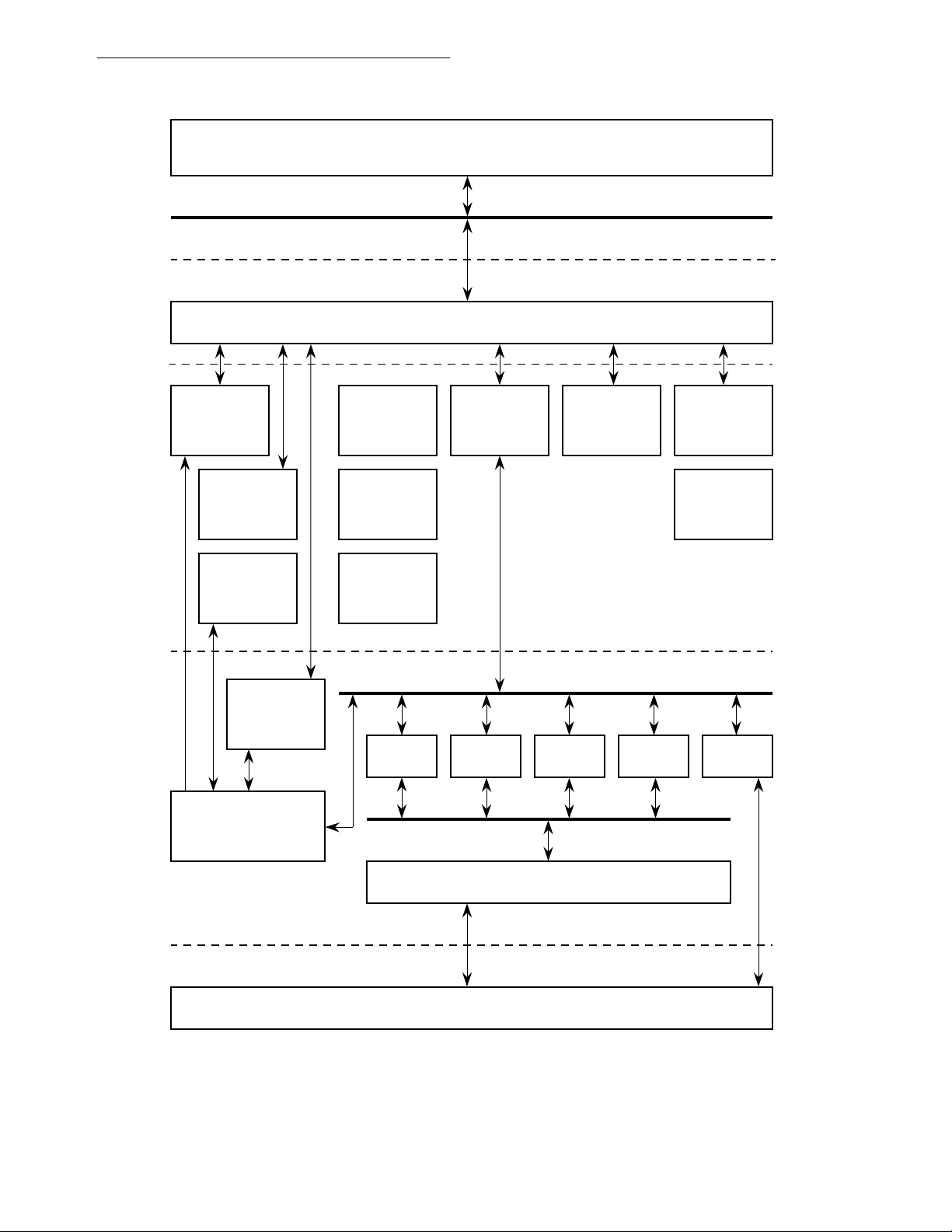
General Description
MC68000/MC68008 CORE
M68000 BUS
MC68000 / MC68008 CORE
ON-CHIP PERIPHERALS BUS INTERFACE UNIT
INTERRUPT
CONTROLLER
1 CHANNEL
IDMA
DRAM
REFRESH
CONTROLLER
MAIN
CONTROLLER
(RISC)
6 CHANNELS
SDMA
BUS ARBITER
3 TIMERS
PARALLEL I/O
PERIPHERAL BUS
SMC (2) SCP
1152 BYTES
DUAL-PORT
STATIC RAM
SCC1 SCC2
CHIP-SELECT
AND WAIT-
STATE LOGIC
SYSTEM INTEGRATION BLOCK
SCC3
SYSTEM
CONTROL
CLOCK
GENERATOR
1-2
SERIAL CHANNELS PHYSICAL INTERFACE
COMMUNICATIONS PROCESSOR
I/O PORTS AND PIN ASSIGNMENTS
Figure 1-1. MC68302 Block Diagram
MC68302 USER’S MANUAL
MOTOROLA

General Description
The MC68302 can also be used in applications such as board-level industrial controllers
performing real-time control applications with a local control bus and an X.25 packet network
connection. Such a system provides the real-time response to a demanding peripheral while
permitting remote monitoring and communication through an X.25 packet network.
1.2 FEATURES
The features of the IMP are as follows:
• On-Chip HCMOS MC68000/MC68008 Core Supporting a 16- or 8-Bit M68000 FamilySystem
• IB Including:
—Independent Direct Memory Access (IDMA) Controller with Three Handshake
Signals:
—Interrupt Controller with Two Modes of Operation
—Parallel Input/Output (I/O) Ports, Some with Interrupt Capability
—On-Chip 1152-Byte Dual-Port RAM
—Three Timers Including a Watchdog Timer
—Four Programmable Chip-Select Lines with Wait-State Generator Logic
—Programmable Address Mapping of the Dual-Port RAM and IMP Registers
—On-Chip Clock Generator with Output Signal
—System Control:
Bus Arbitration Logic with Low-Interrupt Latency Support
System Status and Control Logic
Disable CPU Logic (M68000)
Hardware Watchdog
Low-Power (Standby) Modes
Freeze Control for Debugging
DRAM Refresh Controller
DREQ
,
DACK
, and
DONE
.
• CP Including:
—Main Controller (RISC Processor)
—Three Independent Full-Duplex Serial Communications Controllers (SCCs)
—Supporting Various Protocols:
High-Level/Synchronous Data Link Control (HDLC/SDLC)
Universal Asynchronous Receiver Transmitter (UART)
Binary Synchronous Communication (BISYNC)
Synchronous/Asynchronous Digital Data Communications Message
Protocol (DDCMP)
Transparent Modes
V.110 Rate Adaption
—Six Serial DMA Channels for the Three SCCs
—Flexible Physical Interface Accessible by SCCs Including:
Motorola Interchip Digital Link (IDL)
3
General Circuit Interface (GCI, also known as IOM
-2)
Pulse Code Modulation (PCM) Highway Interface
3.
IOM is a trademark of Siemens AG
MOTOROLA
MC68302 USER’S MANUAL
1-3
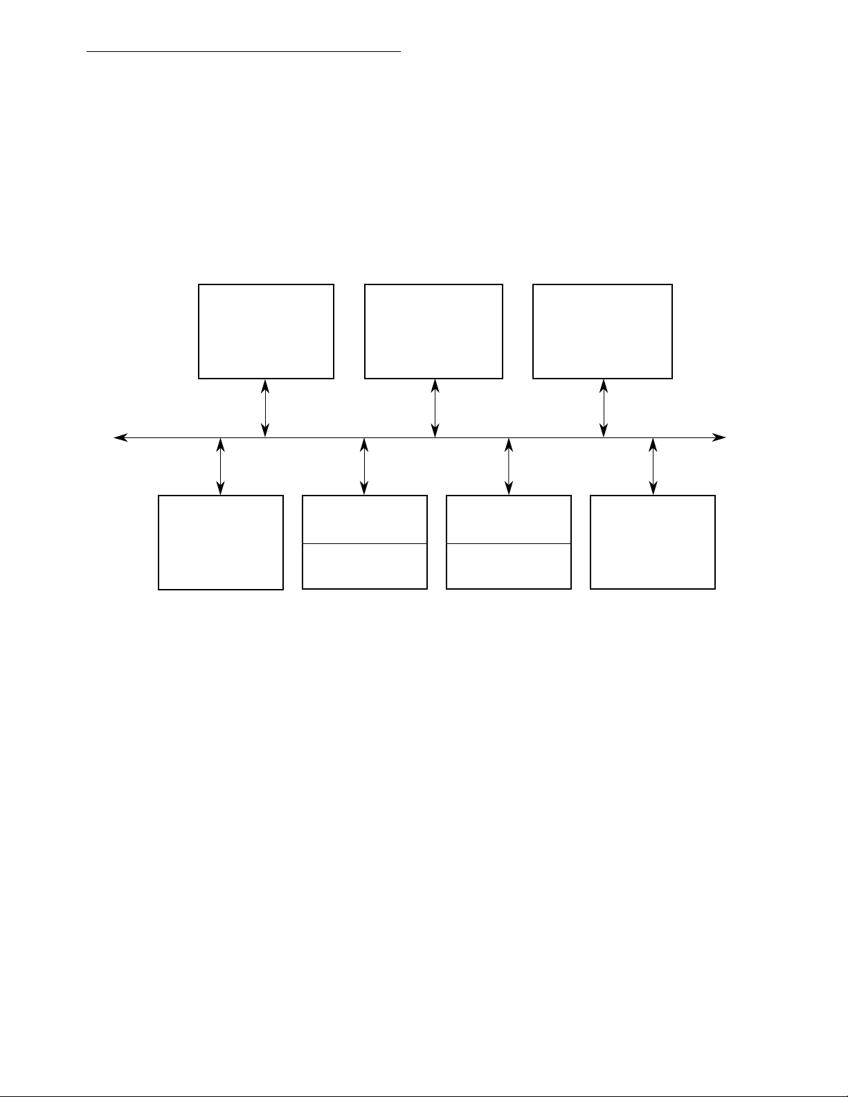
General Description
Nonmultiplexed Serial Interface (NMSI) Implementing Standard Modem Signals
—SCP for Synchronous Communication
—Two Serial Management Controllers (SMCs) To Support IDL and GCI Auxiliary
Channels
1.3 MC68302 SYSTEM ARCHITECTURE
Most general-purpose microprocessor-based systems use an architecture that interfaces all
peripheral devices directly onto a single microprocessor bus (see Figure 1-2).
CPU
SYSTEM BUS
DMA AND/
OR FIFOs
DMA
SERIAL
CHANNELS
ROM
RAM
CPU I/F
ADDITIONAL
DEVICES
TIMERS
Figure 1-2. General-Purpose Microprocessor System Design
The MC68302 microprocessor architecture is shown in Figure 1-3. In this architecture, the
peripheral devices are isolated from the system bus through a dual-port memory. Various
parameters and counters and all memory buffer descriptor tables reside in the dual-port
RAM. The receive and transmit data buffers may be located in the on-chip RAM or in the offchip system RAM. Six DMA channels are dedicated to the six serial ports (receive and transmit for each of the three SCC channels). If data for an SCC channel is programmed to be
located in the external RAM, the CP will program the corresponding DMA channel for the
required accesses, bypassing the dual-port RAM. If data resides in the dual-port RAM, then
the CP accesses the RAM with one clock cycle and no arbitration delays.
1-4
MC68302 USER’S MANUAL
MOTOROLA
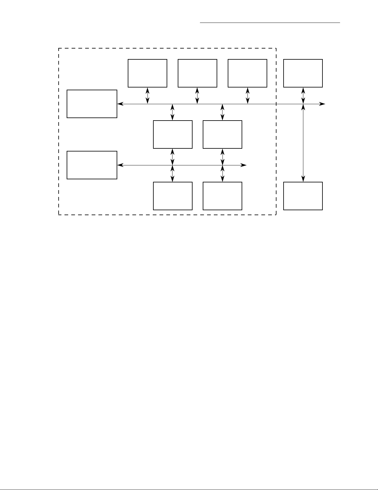
General Description
MC68302 IMP
M68000
CORE
MICROCODED
COMMUNICATIONS
CONTROLLER
(RISC)
INTERRUPT
CONTROLLER
6 DMA
CHANNELS
3 SERIAL
CHANNELS
1 GENERAL-
PURPOSE
DMA
CHANNEL
68000
SYSTEM BUS
1152 BYTES
DUAL-PORT
RAM
PERIPHERAL BUS
OTHER
SERIAL
CHANNELS
3 TIMERS
AND
ADDITIONAL
FEATURES
Figure 1-3. MC68302 System Design
RAM / ROM
OTHER
PERIPHERALS
The use of a unique arbitration scheme and synchronous transfers between the microprocessor and dual-port RAM gives zero wait-state operation to the M68000 microprocessor
core. The dual-port RAM can be accessed by the CP main controller (RISC) once every
clock cycle for either read or write operations. When the M68000 core accesses the dualport RAM, each access is pipelined along with the CP accesses so that data is read or written without conflict. The net effect is the loss of a single memory access by the CP main
controller per M68000 core access.
The buffer memory structure of the MC68302 can be configured to closely match I/O channel requirements by careful selection of buffer size and buffer linking. The interrupt structure
is also programmable so that the on-chip M68000 processor can be off-loaded from the peripheral bit-handling functions to perform higher layer application software or protocol processing.
1.4 NMSI COMMUNICATIONS-ORIENTED ENVIRONMENT
When the interface to equipment or proprietary networks requires the use of standard control and data signals, the MC68302 can be programmed into the nonmultiplexed serial interface (NMSI) mode. This mode, which is available for one, two, or all three SCC ports, can
be selected while the other ports use one of the multiplexed interface modes (IDL, GCI, or
PCM highway).
MOTOROLA
MC68302 USER’S MANUAL
1-5

General Description
In the example shown in Figure 1-4, one SCC channel connects through the NMSI mode to
a commercial packet data network. This connection might be used for remote status monitoring or for maintenance functions for a system. Another SCC is used to connect to a local
asynchronous terminal. The other SCC channel is used as a local synchronous channel,
which could connect to another computer or subsystem. The SCP channel could then be
used for local interconnection of interface chips or peripherals to the MC68302-based system.
1.5 BASIC RATE ISDN OR DIGITAL VOICE/DATA TERMINAL
A basic rate ISDN (2B + D) or digital voice/data terminal can be made from a chip set based
on the MC68302. Refer to Figure 1-5 for an example of a basic rate ISDN voice/data terminal. In this terminal, the CP can directly support the 2B + D channels and perform either
V.110 or V.120 rate adaption. The physical layer serial interface is connected to the local
interconnection bus (IDL in Figure 1-5, but the GCI and PCM buses can also be supported).
The system then supports one of the B channels for voice (connected directly to the physical
bus). The D channel consists of one SCC port; the other B channel is used for data transfer
through a second SCC port. The data can be routed to a terminal (RS-232 type) via the third
SCC port in the NMSI mode. The SCP functions as a control channel for the IDL bus in this
case.
Some ISDN physical layer devices support the signaling and framing functions of the D
channel. In these cases, the D channel can connect through the microprocessor interface
to the physical layer device, and the extra SCC port can then be used for a second B channel
to transfer data.
The benefit of a local interconnection bus (see Figure 1-5) versus a microprocessor bus is
a lower pin count. It is also easy to maintain this low pin-count interface between several
different interface chips, such as the MC145554 PCM codec/filter monocircuit and the
MC145474 S/T transceiver.
The MC68302 combines the M68000 architecture with a number of peripherals for integrated applications in communications control. The M68000 core manages the CP through the
on-chip, dual-port RAM and internal registers. The base address of the dual-port RAM and
internal registers is selected through the base address register. Other peripherals are also
accessed and controlled through internal registers: the IDMA controller, the three timers,
I/O ports, and the interrupt controller.
1-6
MC68302 USER’S MANUAL
MOTOROLA
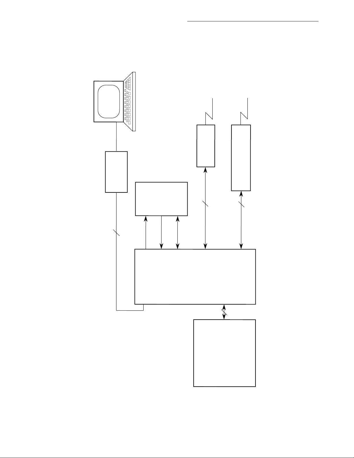
General Description
X.25 WIDE AREA
NETWORK
(E.G., REMOTE
STATUS REPORTS)
MODEM
LOCAL SYNCHRONOUS
CONNECTION
(E.G., COMPUTER TO
COMPUTER INTERCONNECT)
LOCAL
RS232
DRIVER
ADDRESS
NMSI INTERFACE 7
SCC
ROM
PROGRAM
DATA
CONTROL
MC68302
NMSI INTERFACE 7
SCC
IMP
DRIVER/RECEIVERS
NMSI INTERFACE 4
SCC
SCP
3
MOTOROLA
–––––
SENSORS
LOCAL SERIAL
PORT
BOARDS,
OTHER CIRCUIT
VLSI, OR EXTERNAL
Figure 1-4. NMSI Communications-Oriented Board Design
MC68302 USER’S MANUAL
1-7
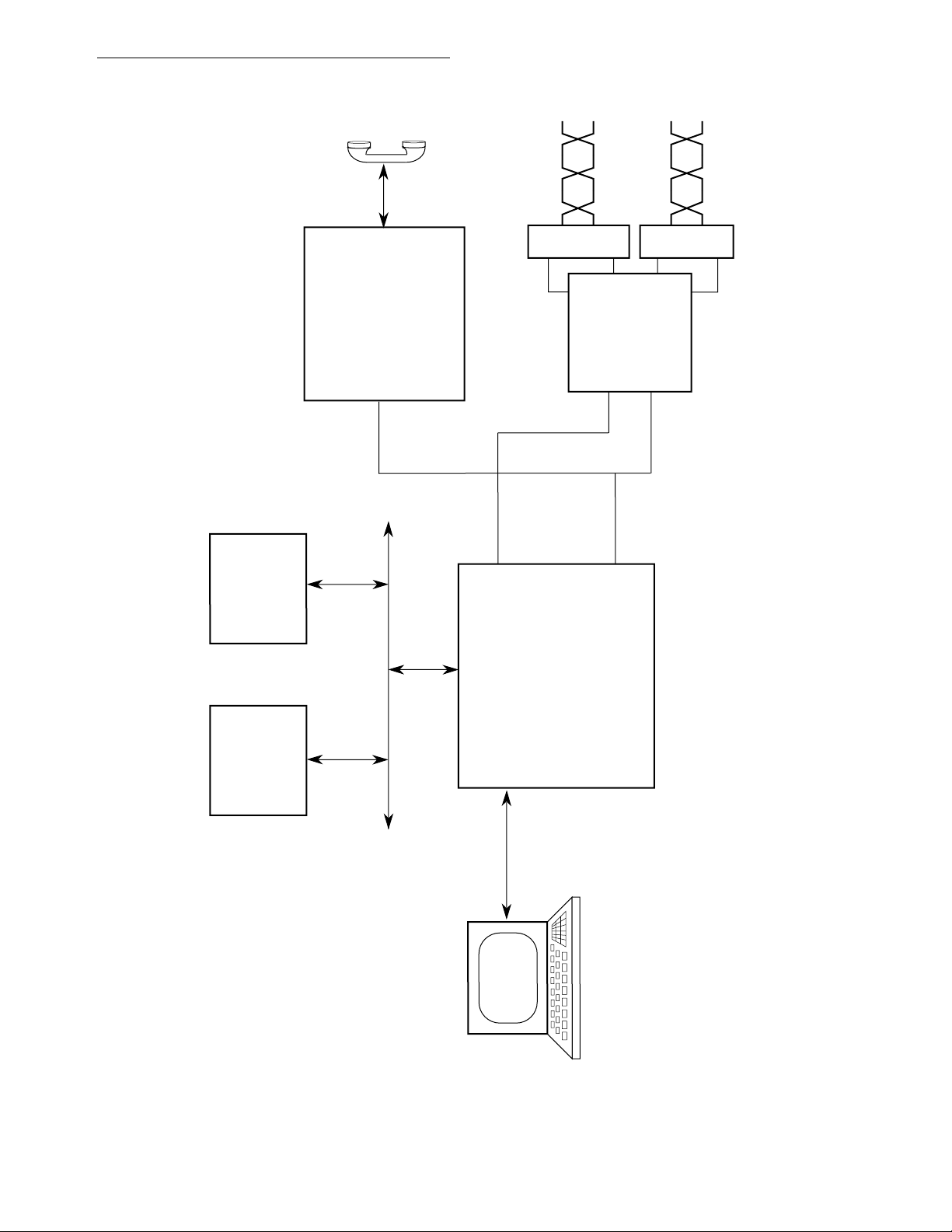
General Description
POTS
FOUR WIRE
PCM
MC145554
CODEC/FILTER
MONOCIRCUIT
MC145474
ICL
(CONTROL)
S/T
TRANSCEIVER
B1+B2+D
EPROM
RAM
B1
M68000 BUS
SCP
M68000/DMA/CS
SCC
BISYNC/
ASYNCHRONOUS/
IMP
MC68302
DDCMP
IDL
(DATA)
SCC
B2+D
SCC
1-8
Figure 1-5. Basic Rate IDL Voice/Data Terminal in ISDN
MC68302 USER’S MANUAL
MOTOROLA

SECTION 2
MC68000/MC68008 CORE
The MC68302 integrates a high-speed M68000 processor with multiple communications peripherals. The provision of direct memory access (DMA) control and link layer management
with the serial ports allows high throughput of data for communications-intensive applications, such as basic rate Integrated Services Digital Network (ISDN).
The MC68302 can operate either in the full MC68000 mode with a 16-bit data bus or in the
MC68008 mode with an 8-bit data bus by tying the bus width (BUSW) pin low. UDS
tions as A0 and LDS
/DS functions as DS in the MC68008 mode.
/A0 func-
NOTE
The BUSW pin is static and is not intended to be used for dynamic bus sizing. If the state of BUSW is changed during operation of the MC68302, erratic operation may occur.
Refer to the MC68000UM/AD,
complete details of the on-chip microprocessor. Throughout this manual, references may
use the notation M68000, meaning all devices belonging to this family of microprocessors,
or the notation MC68000, MC68008, meaning the specific microprocessor products.
M68000 8-/16-/32-Bit Microprocessors User's Manual
, for
2.1 PROGRAMMING MODEL
The M68000 microprocessor executes instructions in one of two modes: user or supervisor.
The user mode provides the execution environment for most of the application programs.
The supervisor mode, which allows some additional instructions and privileges, is intended
for use by the operating system and other system software.
Shown in Figure 2-1, the M68000 core programming model offers 16, 32-bit, general-purpose registers (D7–D0, A7–A0), a 32-bit program counter (PC), and an 8-bit condition code
register (CCR) when running in user space. The first eight registers (D7–D0) are used as
data registers for byte (8-bit), word (16-bit), and long-word (32-bit) operations. The second
set of seven registers (A6–A0) and the stack pointer (USP in user space) may be used as
software stack pointers and base address registers. In addition, the address registers may
be used for word and long-word operations. All 16 registers may be used as index registers.
MOTOROLA
MC68302 USER’S MANUAL
2-1

MC68000/MC68008 Core
31 016 15 8 7
D0
D1
D2
D3
D4
D5
D6
D7
DATA
REGISTERS
31
31
31
16 15
15
7
15
87
CCR
0
A0
A1
A2
A3
A4
A5
A6
0
A7
(USP)
0
PC
0
CCR
031
A7'
(SSP)
0
SR
ADDRESS
REGISTERS
USER STACK
POINTER
PROGRAM
COUNTER
CONDITION
CODE
REGISTER
SUPERVISOR
STACK
POINTER
STATUS
REGISTER
USER
MODE
SUPERVISOR
MODE
Figure 2-1. M68000 Programming Model
The supervisor's programming model includes supplementary registers, including the supervisor stack pointer (SSP) and the status register (SR) as shown in Figure 2-2. The SR
contains the interrupt mask (eight levels available) as well as the following condition codes:
overflow (V), zero (Z), negative (N), carry (C), and extend (X). Additional status bits indicate
that the processor is in trace (T) mode and/or in a supervisor (S) state.
2-2
MC68302 USER’S MANUAL
MOTOROLA

MC68000/MC68008 Core
SYSTEM
BYTE
T S I2 I1 I0 CVZNX
TRACE
MODE
SUPERVISOR
STATE
INTERRUPT
MASK
EXTEND
NEGATIVE
CONDITION
CODES
ZERO
OVERFLOW
CARRY
Figure 2-2. M68000 Status Register
2.2 INSTRUCTION SET SUMMARY
USER
BYTE
048101315
The five data types supported by the M68000 on the MC68302 are bits, binary-coded decimal (BCD) digits (4 bits), bytes (8 bits), words (16 bits), and long words (32 bits).
In addition, operations on other data types, such as memory addresses, status word data,
etc., are provided for in the instruction set. Shown in Table 2-1, the 14 flexible addressing
modes include six basic types:
• Register Direct
• Register Indirect
• Absolute
• Immediate
• Program Counter Relative
• Implied
The capability to perform postincrementing, predecrementing, offsetting, and indexing is included in the register indirect addressing modes. Program counter relative modes can also
be modified via indexing and offsetting.
The M68000 instruction set is shown in Table 2-2.
Some basic instructions also have variations as shown in Table 2-3.
Special emphasis has been placed on the instruction set to simplify programming and to
support structured high-level languages. With a few exceptions, each instruction operates
MOTOROLA
MC68302 USER’S MANUAL
2-3

MC68000/MC68008 Core
on bytes, words, or long words, and most instructions can use any of the 14 addressing
modes.
Combining instruction types, data types, and addressing modes provides over 1000 useful
instructions. These instructions include signed and unsigned multiply and divide, quick arithmetic operations, BCD arithmetic, and expanded operations (through traps).
Table 2-1. M68000 Data Addressing Modes
Mode Generation
Register Direct Addressing
Data Register Direct
Address Register Direct
Absolute Data Addressing
Absolute Short
Absolute Long
Program Counter Relative Addressing
Relative with Offset
Relative with Index and Offset
Register Indirect Addressing
Register Indirect
Postincrement Register Indirect
Predecrement Register Indirect
Register Indirect with Offset
Indexed Register Indirect with Offset
EA = Dn
EA = An
EA = (Next Word)
EA = (Next Two Words)
EA = (PC) + d
EA = (PC) + Xn + d8
EA = (An)
EA = (An), An ⇐ An + N
EA = ← An - N, EA = (An)
EA = (An) + d16
EA = (An) + (Xn) + d8
16
NOTES:
Immediate Data Addressing
Immediate
Quick Immediate
Implied Addressing
Implied Register EA = SR, USP, SSP, PC
EA
An
Dn
Xn
SR
PC
( )
d
8
d16
N
←
Effective Address
=
Address Register
=
Data Register
=
Address or Data Register Used as an Index Register
=
Status Register
=
Program Counter
=
Contents of
=
8-Bit Offset (Displacement)
=
16-Bit Offset (Displacement)
=
1 for byte, 2 for word, and 4 for long word. If An is the stack pointer and the
=
operand size is byte, N = 2 to keep the stack pointer on a word boundary.
Replaces
=
DATA = Next Word(s)
Inherent Data
2-4
MC68302 USER’S MANUAL
MOTOROLA

MC68000/MC68008 Core
Table 2-2. M68000 Instruction Set Summary
Mnemonic
ABCD
ADD
AND
ASL
ASR
Bcc
BCHG
BCLR
BRA
BSET
BSR
BTST
CHK
CLR
CMP
DBcc
DIVS
DIVU
EOR
EXG
EXT
Description Mnemonic Description
Add Decimal with Extend
Add
Logical AND
Arithmetic Shift Left
Arithmetic Shift Right
Branch Conditionally
Bit Test and Change
Bit Test and Clear
Branch Always
Bit Test and Set
Branch to Subroutine
Bit Test
Check Register Against Bounds
Clear Operand
Compare
Decrement and Branch Conditionally
Signed Divide
Unsigned Divide
Exclusive OR
Exchange Registers
Sign Extend
MOVE
MULS
MULU
NBCD
NEG
NOP
NOT
OR Logical OR
PEA Push Effective Address
RESET
ROL
ROR
ROXL
ROXR
RTE
RTR
RTS
Move Source to Destination
Signed Multiply
Unsigned Multiply
Negate Decimal with Extend
Negate
No Operation
Ones Complement
Reset External Devices
Rotate Left without Extend
Rotate Right without Extend
Rotate Left with Extend
Rotate Right with Extend
Return from Exception
Return and Restore
Return from Subroutine
JMP
JSR
LEA
LINK
LSL
LSR
Jump
Jump to Subroutine
Load Effective Address
Link Stack
Logical Shift Left
Logical Shift Right
SBCD
Scc
STOP
SUB
SWAP
TAS
TRAP
TRAPV
TST
UNLK Unlink
Subtract Decimal with Extend
Set Conditionally
Stop
Subtract
Swap Data Register Halves
Test and Set Operand
Trap
Trap on Overflow
Test
MOTOROLA
MC68302 USER’S MANUAL
2-5

MC68000/MC68008 Core
Table 2-3. M68000 Instruction Type Variations
Instruction
Type
ADD
AND
CMP
EOR
MOVE
Variation Description
ADD
ADDA
ADDQ
ADDI
ADDX
AND
ANDI
ANDI to CCR
ANDI to SR
CMP
CMPA
CMPM
CMPI
EOR
EORI
EORI to CCR
EORI to SR
MOVE
MOVEA
MOVEM
MOVEP
MOVEQ
MOVE from SR
MOVE to SR
MOVE to CCR
MOVE USP
Add
Add Address
Add Quick
Add Immediate
Add with Extend
Logical AND
And Immediate
And Immediate to Condition Codes
And Immediate to Status Registers
Compare
Compare Addresses
Compare Memory
Compare Immediate
Exclusive OR
Exclusive OR Immediate
Exclusive OR Immediate to Condition Codes
Exclusive OR Immediate to Status Register
Move Source to Destination
Move Address
Move Multiple Register
Move Peripheral Data
Move Quick
Move from Status Register
Move to Status Register
Move to Condition Codes
Move User Stack Pointer
NEG
OR
SUB
NEG
NEGX
OR
ORI
ORI to CCR
ORI to SR
SUB
SUBA
SUBI
SUBQ
SUBX
Negate
Negate with Extend
Logical OR
OR Immediate
OR Immediate to Condition Codes
OR Immediate to Status Register
Subtract
Subtract Address
Subtract Immediate
Subtract Quick
Subtract with Extend
2.3 ADDRESS SPACES
The M68000 microprocessor operates in one of two privilege states: user or supervisor. The
privilege state determines which operations are legal, which operations are used by the external memory management device to control and translate accesses, and which operations
are used to choose between the SSP and the USP in instruction references. The M68000
address spaces are shown in Table 2-4.
In the M68000 Family, the address spaces are indicated by function code pins. On the
M68000, three function code pins are output from the device on every bus cycle of every
executed instruction. This provides the purpose of each bus cycle to external logic.
2-6
MC68302 USER’S MANUAL
MOTOROLA

*
MC68000/MC68008 Core
Other bus masters besides the M68000 may also output function codes during their bus cycles. On the MC68302, this capability is provided for each potential internal bus master (i.e.,
the IDMA, SDMA, and DRAM refresh units). Also on the MC68302, provision is made for the
decoding of function codes that are output from external bus masters (e.g., in the chip-select
generation logic).
In computer design, function code information can be used to protect certain portions of the
address map from unauthorized access or even to extend the addressable range beyond
the M68000 16-Mbyte address limit. However, in controller applications, function codes are
used most often as a debugging aid. Furthermore, in many controller applications, the
M68000 stays continuously in the supervisor state.
Table 2-4. M68000 Address Spaces
Function Code Output
FC2 FC1 FC0 Reference Class
1 0 0 (Unassigned)
0 0 1 User Data
0 1 0 User Program
0 1 1 (Unassigned)
1 0 0 (Unassigned)
1 0 1 Supervisor Data
1 1 0 Supervisor Program
1
* This is the function code output for the M68000 interrupt
acknowledge cycle.
1
1
CPU Space
All exception processing occurs in the supervisor state, regardless of the state of the S bit
when the exception occurs. The bus cycles generated during exception processing are classified as supervisor references. All stacking operations during exception processing use the
SSP.
The user state is the lower state of privilege. For instruction execution, the user state is determined by the S bit of the SR; if the S bit is negated (low), the processor is executing instructions in the user state. Most instructions execute identically in either user state or
supervisor state. However, instructions having important system effects are privileged. User
programs are not permitted to execute the STOP instruction or the RESET instruction. To
ensure that a user program cannot enter the supervisor state except in a controlled manner,
the instructions which modify the entire SR are privileged. To aid in debugging programs to
be used in operating systems, the move-to-user-stack-pointer (MOVE to USP) and movefrom-user-stack-pointer (MOVE from USP) instructions are also privileged.
The supervisor state is the highest state of privilege. For instruction execution, the supervisor state is determined by the S bit of the SR; if the S bit is asserted (high), the processor is
in the supervisor state. The bus cycles generated by instructions executed in the supervisor
state are classified as supervisor references. While the processor is in the supervisor privilege state, those instructions using either the system stack pointer implicitly or address register seven explicitly access the SSP.
MOTOROLA
MC68302 USER’S MANUAL
2-7

MC68000/MC68008 Core
Once the processor is in the user state and executing instructions, only exception processing can change the privilege state. During exception processing, the current state of the S
bit in the SR is saved and the S bit is asserted, putting the processor in the supervisor state.
Therefore, when instruction execution resumes at the address specified to process the exception, the processor is in the supervisor privilege state. The transition from the supervisor
to user state can be accomplished by any of four instructions: return from exception (RTE),
move to status register (MOVE to SR), AND immediate to status register (ANDI to SR), and
exclusive OR immediate to status register (EORI to SR).
2.4 EXCEPTION PROCESSING
The processing of an exception occurs in four steps, with variations for different exception
causes. During the first step, a temporary copy of the SR is made, and the SR is set for exception processing. During the second step, the exception vector is determined; during the
third step, the current processor context is saved. During the fourth step, a new context is
obtained, and the processor switches to instruction processing.
2.4.1 Exception Vectors
Exception vectors are memory locations from which the processor fetches the address of a
routine to handle that exception. All exception vectors are two words long except for the reset vector, which is four words. All exception vectors lie in the supervisor data space except
for the reset vector, which is in the supervisor program space. A vector number is an 8-bit
number which, when multiplied by four, gives the offset of the exception vector. Vector numbers are generated internally or externally, depending on the cause of the exception. In the
case of interrupts, during the interrupt acknowledge bus cycle, a peripheral may provide an
8-bit vector number to the processor on data bus lines D7–D0. Alternatively, the peripheral
may assert autovector (AVEC
) instead of data transfer acknowledge (DTACK) to request an
autovector for that priority level of interrupt. The exception vector assignments for the
M68000 processor are shown in Table 2-5.
Table 2-5. M68000 Exception Vector Assignment
Vector
Number
0
1
2
3 12 00C SD Address Error
4 16 010 SD Illegal Instruction
5 20 014 SD Zero Divide
6 24 018 SD CHK Instruction
7 28 01C SD TRAPV Instruction
8 32 020 SD Privilege Violation
9 36 024 SD Trace
10 40 028 SD Line 1010 Emulator
Decimal
0 000 SP
4 004 SP
8 008 SD Bus Error
Address
Hex
Space Assignment
Reset: Initial SSP
Reset: Initial PC
2
2
2-8
MC68302 USER’S MANUAL
MOTOROLA
Table 2-5. M68000 Exception Vector Assignment
11 44 02C SD Line 1111 Emulator
MC68000/MC68008 Core
1
12
1
13
1
14
15 60 03C SD Uninitialized Interrupt Vector
1
16–23
24 96 060 SD
25 100 064 SD Level 1 Interrupt Autovector
26 104 068 SD Level 2 Interrupt Autovector
27 108 06C SD Level 3 Interrupt Autovector
28 112 070 SD Level 4 Interrupt Autovector
29 116 074 SD Level 5 Interrupt Autovector
30 120 078 SD Level 6 Interrupt Autovector
31 124 07C SD Level 7 Interrupt Autovector
32–47
1
48–63
64–255
NOTES:
1. Vector numbers 12–14, 16–23, and 48–63 are reserved for future enhancements by Motorola
(with vectors 60–63 being used by the M68302 (see 2.7 MC68302 IMP Configuration and
Control)). No user peripheral devices should be assigned these numbers.
2. Unlike the other vectors which only require two words, reset vector (0) requires four words and is
located in the supervisor program space.
3. The spurious interrupt vector is taken when there is a bus error indication during interrupt
processing.
4. TRAP # n uses vector number 32 + n.
48 030 SD (Unassigned, Reserved)
52 034 SD (Unassigned, Reserved)
56 038 SD (Unassigned, Reserved)
64 040 SD
92 05C SD
128 080 SD
188 0BC SD
192 0C0 SD
255 0FC SD
256 100 SD
1020 3FC SD
(Unassigned, Reserved)
Spurious Interrupt
TRAP Instruction Vectors
(Unassigned, Reserved)
User Interrupt Vectors
3
4
2.4.2 Exception Stacking Order
Exception processing saves the most volatile portion of the current processor context on top
of the supervisor stack. This context is organized in a format called the exception stack
frame. The amount and type of information saved on the stack is determined by the type of
exception. The reset exception causes the M68000 to halt current execution and to read a
new SSP and PC as shown in Table 2-5. A bus error or address error causes the M68000
to store the information shown in Figure 2-3. The interrupts, traps, illegal instructions, and
trace stack frames are shown in Figure 2-4.
MOTOROLA
MC68302 USER’S MANUAL
2-9

MC68000/MC68008 Core
15
ACCESS ADDRESS HIGH
ACCESS ADDRESS LOW
INSTRUCTION REGISTER
STATUS REGISTER
PROGRAM COUNTER HIGH
PROGRAM COUNTER LOW
R/
W
(read/write): write = 0, read = 1
I/N (instruction not): instruction = 0, not =1
FC: Function Code
5 4 3 2 0
R/ W I/N
Figure 2-3. M68000 Bus/Address Error Exception Stack Frame
EVEN BYTE ODD BYTE
77
15
SSP
00
STATUS REGISTER
FC
0
HIGHER
ADDRESS
PROGRAM COUNTER HIGH
PROGRAM COUNTER LOW
Figure 2-4. M68000 Short-Form Exception Stack Frame
NOTE
The MC68302 uses the exact same exception stack frames as
the MC68000.
For exception processing times and instruction execution times,
refer to MC68000UM/AD,
Manual
.
8-/16-/32-Bit Microprocessor User's
2-10
MC68302 USER’S MANUAL
MOTOROLA

MC68000/MC68008 Core
2.5 INTERRUPT PROCESSING
Seven interrupt levels are provided by the M68000 core. If the IMP's interrupt controller is
placed in the normal mode, six levels are available to the user. If the interrupt controller is in
the dedicated mode, three levels are available to the user. In either mode, level 4 is reserved
for the on-chip peripherals. Devices may be chained externally within one of the available
priority levels, allowing an unlimited number of external peripheral devices to interrupt the
processor. The SR contains a 3-bit mask indicating the current processor priority level. Interrupts are inhibited for all priority levels less than or equal to the current processor priority
(see Figure 2-2).
An interrupt request is made to the processor by encoding the request on the interrupt request lines (normal mode) or by asserting the appropriate request line (dedicated mode).
Rather than forcing immediate exception processing, interrupt requests arriving at the processor are made pending to be detected between instruction executions.
If the priority of the pending interrupt is lower than or equal to the current processor priority,
execution continues with the next instruction, and the interrupt exception processing is postponed.
If the priority of the pending interrupt is greater than the current processor priority, the exception processing sequence is started. A copy of the SR is saved, the privilege state is set
to supervisor state, tracing is suppressed, and the processor priority level is set to the level
of the interrupt being acknowledged. The processor fetches the vector number from the interrupting device, classifying the reference as an interrupt acknowledge on the address bus.
If external logic requests automatic vectoring (via the AVEC
pin), the processor internally
generates a vector number determined by the interrupt level number. If external logic indicates a bus error, the interrupt is considered spurious, and the generated vector number references the spurious interrupt vector number.
2.6 M68000 SIGNAL DIFFERENCES
The MC68302 core supports one additional signal not visible on the standard M68000:
. Asserted externally on read-modify-write cycles, the RMC signal is typically used as
RMC
a bus lock to ensure integrity of instructions using the locked read-modify-write operation of
the test and set (TAS) instruction. The RMC
MC68302 arbiter and can be programmed to prevent the arbiter from issuing bus grants until
the completion of an MC68000-core-initiated read-modify-write cycle.
The MC68302 can be programmed to use the RMC
the end of the read portion of the cycle and assert AS
of the cycle (See 3.8.3 System Control Bits).
signal from the M68000 core is applied to the
signal to negate address strobe (AS) at
at the beginning of the write portion
Two M6800 signals are omitted from the MC68302: valid memory address (VMA
able (E). The valid peripheral address (VPA
MC68302 as AVEC
to direct the core to use an autovector during interrupt acknowledge cy-
) signal is retained, but is only used on the
cles.
MOTOROLA
MC68302 USER’S MANUAL
) and en-
2-11

MC68000/MC68008 Core
2.7 MC68302 IMP CONFIGURATION CONTROL
Four reserved entries in the external M68000 exception vector table (see Table 2-5) are
used as addresses for internal system configuration registers. These entries are at locations
$0F0, $0F4, $0F8, and $0FC. The first entry is the on-chip peripheral base address register
(BAR) entry; the second is the on-chip system control register (SCR) entry; the least significant word of the third entry is the clock control register (CKCR), and fourth entry is reserved
for future use.
The BAR entry contains the BAR described in this section. The SCR entry contains the SCR
described in 3.8.1 System Control Register (SCR). The CKCR entry contains the CKCR register described in 3.9 Clock Control Register.
Figure 2-5 shows all the MC68302 IMP on-chip addressable locations and how they are
mapped into system memory.
SYSTEM MEMORY MAP
$0
EXCEPTION
VECTOR
TABLE
MC68302
$0F0
$0F4
$0F8
$0FC
BASE + $0
BAR ENTRY
SCR ENTRY
CKCR ENTRY
RESERVED
4K BLOCK
SYSTEM RAM
(DUAL-PORT)
$3FF
BAR
POINTS
TO THE
BASE
256 VECTOR
ENTRIES
BASE + $400
PARAMETER RAM
(DUAL-PORT)
BASE + $800
INTERNAL
REGISTERS
BASE + $FFF
$xxx000 = BASE
4K BLOCK
$FFFFFF
Figure 2-5. MC68302 IMP Configuration Control
The on-chip peripherals, including those peripherals in both the CP and SIB, require a 4Kbyte block of address space. This 4K-byte block location is determined by writing the intended base address to the BAR in supervisor data space (FC = 5). The address of the BAR en-
2-12
MC68302 USER’S MANUAL
MOTOROLA

MC68000/MC68008 Core
try is $0F0; however, the actual BAR is a 16-bit value within the BAR entry and is located at
$0F2.
After a total system reset, the on-chip peripheral base address is undefined, and it is not
possible to access the on-chip peripherals at any address until BAR is written. The BAR and
the SCR can always be accessed at their fixed addresses.
NOTE
The BAR, SCR and CKCR registers are internally reset only
when a total system reset occurs by the simultaneous assertion
of RESET and
HALT. The chip-select (CS) lines are not asserted on accesses to these locations. Thus, it is very helpful to use
CS lines to select external ROM/RAM that overlaps the BAR and
SCR register locations, since this prevents potential bus contention. (The internal access (IAC) signal may also be used to prevent bus contention.)
NOTE
In 8-bit system bus operation, IMP accesses are not possible until the low byte of the BAR is written. Since the MOVE.W instruction writes the high byte followed by the low byte, this instruction
guarantees the entire word is written.
Do not assign other devices on the system bus an address that falls within the address
range of the peripherals defined by the BAR. If this happens, BERR
is generated (if the address decode conflict enable (ADCE) bit is set) and the address decode conflict (ADC) bit in
the SCR is set.
The BAR is a 16-bit, memory-mapped, read-write register consisting of the high address
bits, the compare function code bit, and the function code bits. Upon a total system reset, its
value may be read as $BFFF, but its value is not valid until written by the user. The address
of this register is fixed at $0F2 in supervisor data space. BAR cannot be accessed in user
data space.
15 13 12 11 0
FC2–FC0 CFC
23 22 21 20 19 18 17 16 15 14 13 12
BASE ADDRESS
Bits 15–13—FC2–FC0
The FC2–FC0 field is contained in bits 15–13 of the BAR. These bits are used to set the
address space of 4K-byte block of on-chip peripherals. The address compare logic uses
these bits, dependent upon the CFC bit, to cause an address match within its address
space.
MOTOROLA
NOTE
Do not assign this field to the M68000 core interrupt acknowledge space (FC2–FC0 = 7).
MC68302 USER’S MANUAL
2-13
MC68000/MC68008 Core
CFC—Compare Function Code
0 = The FC bits in the BAR are ignored. Accesses to the IMP 4K-byte block occur with-
out comparing the FC bits.
1 = The FC bits in the BAR are compared. The address space compare logic uses the
FC bits to detect address matches.
Bits 11–0—Base Address
The high address field is contained in bit 11–0 of the BAR. These bits are used to set the
starting address of the dual-port RAM. The address compare logic uses only the most significant bits to cause an address match within its block size.
2.8 MC68302 MEMORY MAP
The following tables show the additional registers added to the M68000 to make up the
MC68302. All of the registers are memory-mapped. Four entries in the M68000 exception
vectors table (located in low RAM) are reserved for addresses of system configuration registers (see Table 2-6) that reside on-chip. These registers have fixed addresses of $0F0–
$0FF. All other on-chip peripherals occupy a 4K-byte relocatable address space. When an
on-chip register or peripheral is accessed, the internal access (IAC) pin is asserted.
Table 2-6. System Configuration Register
Address Name Width Description Reset Value
$0F0
$0F2
*
$0F4
*
$0F8 RES 16 Reserved
$0FA CKCR 16 Clock Control Register 0000
$0FC RES 32 Reserved
*
Reset only upon a total system reset.
RES 16 Reserved
BAR 16 Base Address Register BFFF
SCR 32 System Control Register 0000 0F00
The internal 1176-byte dual-port RAM has 576 bytes of system RAM (see Table 2-7) and
576 bytes of parameter RAM (see Table 2-8).
Table 2-7. System RAM
Address Width Block Description
Base + 000
•
•
•
Base + 23F
Base +240
•
•
•
Base + 3FF
576 Bytes RAM User Data Memory
Reserved
(Not Implemented)
The parameter RAM contains the buffer descriptors for each of the three SCC channels, the
SCP, and the two SMC channels. The memory structures of the three SCC channels are
2-14
MC68302 USER’S MANUAL
MOTOROLA

MC68000/MC68008 Core
identical. When any SCC, SCP, or SMC channel buffer descriptors or parameters are not
used, their parameter RAM area can be used for additional memory. For detailed information about the use of the buffer descriptors and protocol parameters in a specific protocol,
see 4.5 Serial Communication Controllers (SCCs). Base + 67E contains the MC68302 revision number. Revision A parts (mask 1B14M) correspond to the value $0001. Revision B
parts (mask 2B14M and 3B14M which are described in this manual) correspond to the value
$0002. Revision C and D parts have revision number $0003.
Table 2-8. Parameter RAM
Address Width Block Description
Base + 400
Base + 408
Base + 410
Base + 418
Base + 420
Base + 428
Base + 430
Base + 438
Base + 440
Base + 448
Base + 450
Base + 458
Base + 460
Base + 468
Base + 470
Base + 478
Base + 480
•
•
•
Base + 4BF
Base + 4C0
•
•
•
Base + 4FF
Base + 500
Base + 508
Base + 510
Base + 518
Base + 520
Base + 528
Base + 530
Base + 538
Base + 540
Base + 548
Base + 550
Base + 558
Base + 560
Base + 568
Base + 570
Base + 578
4 Word
4 Word
4 Word
4 Word
4 Word
4 Word
4 Word
4 Word
4 Word
4 Word
4 Word
4 Word
4 Word
4 Word
4 Word
4 Word
4 Word
4 Word
4 Word
4 Word
4 Word
4 Word
4 Word
4 Word
4 Word
4 Word
4 Word
4 Word
4 Word
4 Word
4 Word
4 Word
SCC1
SCC1
SCC1
SCC1
SCC1
SCC1
SCC1
SCC1
SCC1
SCC1
SCC1
SCC1
SCC1
SCC1
SCC1
SCC1
SCC1
SCC1
SCC2
SCC2
SCC2
SCC2
SCC2
SCC2
SCC2
SCC2
SCC2
SCC2
SCC2
SCC2
SCC2
SCC2
SCC2
SCC2
Specific Protocol Parameters
Rx BD 0
Rx BD 1
Rx BD 2
Rx BD 3
Rx BD 4
Rx BD 5
Rx BD 6
Rx BD 7
Tx BD 0
Tx BD 1
Tx BD 2
Tx BD 3
Tx BD 4
Tx BD 5
Tx BD 6
Tx BD 7
Reserved
(Not Implemented)
Rx BD 0
Rx BD 1
Rx BD 2
Rx BD 3
Rx BD 4
Rx BD 5
Rx BD 6
Rx BD 7
Tx BD 0
Tx BD 1
Tx BD 2
Tx BD 3
Tx BD 4
Tx BD 5
Tx BD 6/DRAM Refresh
Tx BD 7/DRAM Refresh
MOTOROLA
MC68302 USER’S MANUAL
2-15

MC68000/MC68008 Core
Table 2-8. Parameter RAM
Base + 580
•
•
•
Base + 5BF
Base + 5C0
•
•
•
Base + 5FF
Base + 600
Base + 608
Base + 610
Base + 618
Base + 620
Base + 628
Base + 630
Base + 638
Base + 640
Base + 648
Base + 650
Base + 658
Base + 660
Base + 666
Base + 668
Base + 66A
Base + 66C
Base + 66E #
Base +67A
Base +67C
Base +67E #
Base + 680
•
•
•
Base + 6BF
Base + 6C0
•
•
•
Base + 7FF
4 Word
4 Word
4 Word
4 Word
4 Word
4 Word
4 Word
4 Word
4 Word
4 Word
4 Word
4 Word
3 Word
Word
Word
Word
Word
6 Word
Word
Word
Word
SCC2
SCC2
SCC3
SCC3
SCC3
SCC3
SCC3
SCC3
SCC3
SCC3
SCC3
SCC3
SCC3
SCC3
SMC
SCC1
SCC1
SCC2
SCC2
SMC1–SMC2
SCP
SCC1–SCC3
CP
SCC3
SCC3
Specific Protocol Parameters
Reserved
(Not Implemented)
RxBD0
RxBD1
RxBD2
RxBD3
RxBD4
RxBD5
RxBD6
RxBD7
TxBD0
TxBD1
TxBD2
TxBD3 ##
Reserved
RxBD
TxBD
RxBD
TxBD
Internal Use
Rx/TxBD
BERR Channel Number
MC68302 Revision Number
Specific Protocol Parameters
Reserved
(Not Implemented)
#
Modified by the CP after a CP or system reset.
## Tx BD 4, 5, 6, and 7 are not initially available to SCC3. (See 4.5.5 Buffer Descriptors Table for
information on how they may be regained.)
In addition to the internal dual-port RAM, a number of internal registers support the functions
of the various M68000 core peripherals. The internal registers (see Table 2-9) are memorymapped registers offset from the BAR point1616er and are located on the internal M68000
bus.
2-16
MC68302 USER’S MANUAL
MOTOROLA

MC68000/MC68008 Core
NOTE
All undefined and reserved bits within registers and parameter
RAM values written by the user in a given application should be
written with zero to allow for future enhancements to the device.
Table 2-9. Internal Registers
Address Name Width Block Description Reset Value
Base + 800
Base + 802
Base + 804
Base + 808
Base + 80C
! Base + 80E
Base + 80F
Base + 810
Base + 811
Base + 812 #
! Base + 814
Base + 816
! Base + 818
Base + 81A
Base + 81C
Base + 81E #
Base + 820 #
Base + 822 #
Base + 824 #
Base + 826 #
Base + 828 #
Base + 82A
Base + 82C
Base + 82E
Base + 830 #
Base + 832 #
Base + 834 #
Base + 836 #
Base + 838 #
Base + 83A #
Base + 83C #
Base + 83E #
RES
CMR
SAPR
DAPR
BCR
CSR
RES
FCR
RES
GIMR
IPR
IMR
ISR
RES
RES
PACNT
PADDR
PADAT
PBCNT
PBDDR
PBDAT
RES
RES
RES
BR0
OR0
BR1
OR1
BR2
OR2
BR3
OR3
16
16
32
32
16
8
8
8
8
16
16
16
16
16
16
16
16
16
16
16
16
16
16
16
16
16
16
16
16
16
16
16
IDMA
IDMA
IDMA
IDMA
IDMA
IDMA
IDMA
IDMA
IDMA
Int Cont
Int Cont
Int Cont
Int Cont
Int Cont
Int Cont
PIO
PIO
PIO
PIO
PIO
PIO
PIO
CS
CS
CS0
CS0
CS1
CS1
CS2
CS2
CS3
CS3
Reserved
Channel Mode Register
Source Address Pointer
Destination Address Pointer
Byte Count Register
Channel Status Register
Reserved
Function Code Register
Reserved
Global Interrupt Mode Register
Interrupt Pending Register
Interrupt Mask Register
In-Service Register
Reserved
Reserved
Port A Control Register
Port A Data Direction Register
Port A Data Register
Port B Control Register
Port B Data Direction Register
Port B Data Register Reserved
Reserved
Reserved
Base Register 0
Option Register 0
Base Register 1
Option Register 1
Base Register 2
Option Register 2
Base Register 3
Option Register 3
0000
XXXX XXXX
XXXX XXXX
XXXX
00
XX
0000
0000
0000
0000
0000
0000
XXXX ##
0080
0000
XXXX ##
C001
DFFD
C000
DFFD
C000
DFFD
C000
DFFD
MOTOROLA
MC68302 USER’S MANUAL
2-17

MC68000/MC68008 Core
Table 2-9. Internal Registers
Base + 840
Base + 842
Base + 844
Base + 846
Base + 848
! Base + 849
Base + 84A
Base + 84C
Base + 84E
Base + 850
Base + 852
Base + 854
Base + 856
Base + 858
! Base + 859
Base + 85A
Base + 85C
Base + 85E
Base + 860 CR 8 CP Command Register 00
Base + 861
•
•
•
Base + 87F
Base + 880
Base + 882
Base + 884
Base + 886
! Base + 888
Base + 889
Base + 88A
Base + 88B
Base + 88C
Base + 88D
Base + 88E
TMR1
TRR1
TCR1
TCN1
RES
TER1
WRR
WCN
RES
TMR2
TRR2
TCR2
TCN2
RES
TER2
RES
RES
RES
RES
SCON1
SCM1
DSR1
SCCE1
RES
SCCM1
RES
SCCS1
RES
RES
16
16
16
16
8
8
16
16
16
16
16
16
16
8
8
16
16
16
16
16
16
16
8
8
8
8
8
8
16
Timer
Timer
Timer
Timer
Timer
Timer
WD
WD
Timer
Timer
Timer
Timer
Timer
Timer
Timer
Timer
Timer
Timer
SCC1
SCC1
SCC1
SCC1
SCC1
SCC1
SCC1
SCC1
SCC1
SCC1
SCC1
Timer Unit 1 Mode Register
Timer Unit 1 Reference Register
Timer Unit 1 Capture Register
Timer Unit 1 Counter
Reserved
Timer Unit 1 Event Register
Watchdog Reference Register
Watchdog Counter
Reserved
Timer Unit 2 Mode Register
Timer Unit 2 Reference Register
Timer Unit 2 Capture Register
Timer Unit 2 Counter
Reserved
Timer Unit 2 Event Register
Reserved
Reserved
Reserved
Reserved
(Not Implemented)
Reserved
SCC1 Configuration Register
SCC1 Mode Register
SCC1 Data Sync. Register
SCC1 Event Register
Reserved
SCC1 Mask Register
Reserved
SCC1 Status Register
Reserved
Reserved
0000
FFFF
0000
0000
00
FFFF
0000
0000
FFFF
0000
0000
00
0004
0000
7E7E
00
00
00
Base + 890
Base + 892
Base + 894
Base + 896
! Base + 898
Base + 899
Base + 89A
Base + 89B
Base + 89C
Base + 89D
Base + 89E
2-18
RES
SCON2
SCM2
DSR2
SCCE2
RES
SCCM2
RES
SCCS2
RES
RES
16
16
16
16
8
8
8
8
8
8
16
SCC2
SCC2
SCC2
SCC2
SCC2
SCC2
SCC2
SCC2
SCC2
SCC2
SCC2
MC68302 USER’S MANUAL
Reserved
SCC2 Configuration Register
SCC2 Mode Register
SCC2 Data Sync. Register
SCC2 Event Register
Reserved
SCC2 Mask Register
Reserved
SCC2 Status Register
Reserved
0004
0000
7E7E
00
00
00
MOTOROLA

Table 2-9. Internal Registers
MC68000/MC68008 Core
Base + 8A0
Base + 8A2
Base + 8A4
Base + 8A6
! Base + 8A8
Base + 8A9
Base + 8AA
Base + 8AB
Base + 8AC
Base + 8AD
Base + 8AE
Base + 8B0 SPMODE 16 SCM
Base + 8B2 #
Base + 8B4 #
Base + 8B6
•
•
•
Base + FFF
# Reset only upon a total system reset (RESET and HALT assert together), but not on the execution of an M68000
RESET instruction. See the RESET pin description for details.
## The output latches are undefined at total system reset.
! Event register with special properties (see 2.9 Event Registers).
RES
SCON3
SCM3
DSR3
SCCE3
RES
SCCM3
RES
SCCS3
RES
RES
SIMASK
SIMODE
16
16
16
16
8
8
8
8
8
8
16
16
16
SCC3
SCC3
SCC3
SCC3
SCC3
SCC3
SCC3
SCC3
SCC3
SCC3
SCC3
SI
SI
Reserved
SCC3 Configuration Register
SCC3 Mode Register
SCC3 Data Sync. Register
SCC3 Event Register
Reserved
SCC3 Mask Register
Reserved
SCC3 Status Register
Reserved
Reserved
SCP, SMC Mode and Clock
Control Register
Serial Interface Mask Register
Serial Interface Mode Register
Reserved
(Not Implemented)
0004
0000
7E7E
00
00
00
0000
FFFF
0000
2.9 EVENT REGISTERS
The IMP contains a few special registers designed to report events to the user. They are the
channel status register (CSR) in the independent DMA, the interrupt pending register (IPR)
and interrupt in-service register (ISR) in the interrupt controller, the timer event register 1
(TER1) in timer 1, the TER2 in timer 2, serial communication controller event register 1
(SCCE1) in SCC1, SCCE2 in SCC2, and SCCE3 in SCC3. Events in these register are always reported by a bit being set.
During the normal course of operation, the user software will clear these events after recognizing them. To clear a bit in one of these registers, the user software must WRITE A ONE
TO THAT BIT. Writing a zero has no effect on the register. Thus, in normal operation, the
sets
hardware only
bits in these registers; whereas, the software only
This technique prevents software from inadvertently losing the indication from an event bit
that is “set” by the hardware between the software read and the software write of this register.
All these registers are cleared after a total system reset (RESET
and HALT asserted together) and after the M68000 RESET instruction. Also some of the blocks (IDMA, timer1, timer2,
and communication processor) have a reset (RST) bit located in a register in that block. This
RST bit will reset that entire block, including any event registers contained therein.
clears
them.
Examples:
1. To clear bit 0 of SCCE1, execute "MOVE.B #$01,SCCE1"
MOTOROLA
MC68302 USER’S MANUAL
2-19

MC68000/MC68008 Core
2. To clear bits 0 and 1 of SCC1, execute "MOVE.B #$03,SCCE1”
3. To clear all bits in SCCE1, execute "MOVE.B #$ff,SCCE1"
where SCCE1 is equated to the actual address of SCCE1.
NOTE
DO NOT use read-modify-write instructions to clear bits in an
event register, or ALL bits in that register will inadvertently be
cleared. Read-modify-write instructions include BSET, BCLR,
AND, OR, etc. These instructions read the contents of a location,
perform an operation, and write the result back, leaving the rest
of the bits unchanged. Thus, if a bit is a one when read, it will be
written back with a one, clearing that bit. For example, the instruction “BSET.B #0,SCCE1” will actually clear ALL bits in
SCCE1, not just bit 0.
2-20 MC68302 USER’S MANUAL MOTOROLA

SECTION 3
SYSTEM INTEGRATION BLOCK (SIB)
The MC68302 contains an extensive SIB that simplifies the job of both the hardware and
software designer. It integrates the M68000 core with the most common peripherals used in
an M68000-based system. The independent direct memory access (IDMA) controller relieves the hardware designer of the extra effort and board logic needed to connect an external DMA controller. The interrupt controller can be used in a dedicated mode to generate
interrupt acknowledge signals without external logic. Also, the chip-select signals and their
associated wait-state logic eliminate the need to generate chip-select signals externally. The
three timers simplify control and improve reliability. These and other features in the SIB conserve board space and cost while decreasing development time.
The SIB includes the following functions:
• IDMA Controller with Three Handshake Signals: DREQ
• Interrupt Controller with Two Modes of Operation
• Parallel Input/Output (I/O) Ports, Some with Interrupt Capability
• On-Chip 1152-Byte Dual-Port RAM
• Three Timers Including a Software Watchdog Timer
• Four Programmable Chip-Select Lines with Wait-State Generator Logic
• On-Chip Clock Generator with Output Signal
• System Control
—System Status and Control Logic
—Disable CPU Logic (M68000)
—Bus Arbitration Logic with Low-Interrupt Latency Support
—Hardware Watchdog for Monitoring Bus Activity
—Low-Power (Standby) Modes
—Freeze Control for Debugging
• Clock Control
—Adjustable CLKO Drive
—Three-state RCLK1 and TCLK1
—Disable BRG1
, DACK, and DONE
• DRAM Refresh Controller
MOTOROLA
MC68302 USER’S MANUAL
3-1

System Integration Block (SIB)
3.1 DMA CONTROL
The IMP includes seven on-chip DMA channels, six serial DMA (SDMA) channels for the
three serial communications controllers (SCCs) and one IDMA. The SDMA channels are
discussed in 4.2 SDMA Channels. The IDMA is discussed in the following paragraphs.
3.1.1 Key Features
The IDMA (Independent DMA Controller) has the following key features:
• Two Address Pointers and One Counter
• Support of Memory-to-Memory, Peripheral-to-Memory, and Memory-to-Peripheral Data
Transfers
• Three I/O Lines, DREQ
, DACK, and DONE, for Externally Requested Data Transfers
• Asynchronous M68000 Bus Structure with 24-Bit Address and 8-Bit or 16-Bit Data Bus
• Support for Data Blocks Located at Even or Odd Addresses
• Packing and Unpacking of Operands
• Fast Transfer Rates: Up to 4M bytes/second at 16.0 MHz with No Wait States
• Full Support of All M68000 Bus Exceptions: Halt, Bus Error, Reset, and Retry
• Flexible Request Generation:
—Internal, Maximum Rate (One Burst)
—Internal, Limited Rate (Limited Burst Bandwidth)
—External, Burst (DREQ
—External, Cycle Steal (DREQ
Level Sensitive)
Edge Sensitive)
The one general-purpose IDMA controller can operate in different modes of data transfer as
programmed by the user. The IDMA is capable of transferring data between any combination of memory and I/O. In addition, data may be transferred in either byte or word quantities,
and the source and destination addresses may be either odd or even. Note that the chip select and wait state generation logic on the MC68302 may be used with the IDMA, if desired.
Every IDMA cycle requires between two and four bus cycles, depending on the address
boundary and transfer size. Each bus cycle is a standard M68000-type read or write cycle.
If both the source and destination addresses are even, the IDMA fetches one word of data
and immediately deposits it. If either the source or destination address begins on an odd
boundary, the transfer is handled differently. For example, if the source address starts on an
odd boundary and the destination address is even, the IDMA reads one byte from the
source, then reads the second byte from the source, and finally stores the word in a single
access. If the source is even and the destination odd, then the IDMA will read one word from
the source and store it in two consecutive cycles. If both the source and destination are odd,
the IDMA performs two read byte cycles followed by two write byte cycles until the transfer
is complete.
If the IMP frequency is 16.0 MHz and zero wait state memory is used, then the maximum
transfer rate is 4M byte/sec. This assumes that the operand size is 16-bits, the source and
destination addresses are even, and the bus width is selected to be 16-bits.
3-2
MC68302 USER’S MANUAL
MOTOROLA

System Integration Block (SIB)
The maximum transfer rate is calculated from the fact that 16 bits are moved every 8 clocks.
The calculation is as follows:
16 bits x 16M clocks/sec
(2 bus cycles) x (4 clocks/bus cycle) 8 clocks sec
=
2 bytes x 16M clocks/sec
=
4M bytes
The IDMA controller block diagram is shown in Figure 3-1.
IDBR
IDMA
IDBG
IBCLR
CONTROL
LOGIC
15 0
CHANNEL MODE REGISTER
15 0
BYTE COUNT REGISTER
7
DONE
DACK
DREQ
INTERRUPT REQUEST
0
CHANNEL STATUS REGISTER
SOURCE ADDRESS POINTER REGISTER
M68000 CORE DATA BUS
BUS
CP PERIPHERAL
31 0
DESTINATION ADDRESS POINTER REGISTER
7
FUNCTION CODE REGISTER
15
SDMA DATA REGISTER
31
SDMA ADDRESS AND FC REGISTER
Figure 3-1. IDMA Controller Block Diagram
3.1.2 IDMA Registers (Independent DMA Controller)
031
0
0
M68000 CORE ADDRESS BUS
0
The IDMA has six registers that define its specific operation. These registers include a 32bit source address pointer register (SAPR), a 32-bit destination address pointer register
MOTOROLA
MC68302 USER’S MANUAL
3-3

System Integration Block (SIB)
(DAPR), an 8-bit function code register (FCR), a 16-bit byte count register (BCR), a 16-bit
channel mode register (CMR), and an 8-bit channel status register (CSR). These registers
provide the addresses, transfer count, and configuration information necessary to set up a
transfer. They also provide a means of controlling the IDMA and monitoring its status. All
registers can be modified by the M68000 core. The IDMA also includes another 16-bit register, the data holding register (DHR), which is not accessible to the M68000 core and is
used by the IDMA for temporary data storage.
3.1.2.1 Channel Mode Register (CMR)
The CMR, a 16-bit register, is reset to $0000.
15 14 13 12 11 10 9 8 7 6 5 4 3 2 1 0
— ECO INTN INTE REQG SAPI DAPI SSIZE DSIZE BT RST STR
Bit 15—Reserved for future use.
ECO—External Control Option
0 = If the request generation is programmed to be external in the REQG bits, the con-
trol signals (D
ACK and DONE) are used in the source (read) portion of the transfer
since the peripheral is the source.
1 = If the request generation is programmed to be external in the REQG bits, the con-
trol signals (D
ACK and DONE) are used in the destination (write) portion of the
transfer since the peripheral is the destination.
INTN—Interrupt Normal
0 = When the channel has completed an operand transfer without error conditions as
indicated by DONE
, the channel does not generate an interrupt request to the IMP
interrupt controller. The DONE bit remains set in the CSR.
1 = When the channel has completed an operand transfer without error conditions as
indicated by DONE
, the channel generates an interrupt request to the IMP interrupt
controller and sets DONE in the CSR.
NOTE
An interrupt will only be generated if the IDMA bit is set in the interrupt mask register (IMR).
INTE—Interrupt Error
0 = If a bus error occurs during an operand transfer either on the source read (BES) or
the destination write (BED), the channel does not generate an interrupt to the IMP
interrupt controller. The appropriate bit remains set in the CSR.
1 = If a bus error occurs during an operand transfer either on BES or BED, the channel
generates an interrupt to the IMP interrupt controller and sets the appropriate bit
(BES or BED) in the CSR.
3-4
MC68302 USER’S MANUAL
MOTOROLA

System Integration Block (SIB)
NOTE
An interrupt will only be generated if the IDMA bit is set in the
IMR.
REQG—Request Generation
The following decode shows the definitions for the REQG bits:
00 = Internal request at limited rate (limited burst bandwidth) set by burst transfer (BT)
bits
01 = Internal request at maximum rate (one burst)
10 = External request burst transfer mode (DREQ
11 = External request cycle steal (DREQ
edge sensitive)
level sensitive)
SAPI—Source Address Pointer (SAP) Increment
0 = SAP is not incremented after each transfer.
1 = SAP is incremented by one or two after each transfer, according to the source size
(SSIZE) bits and the starting address.
DAPI—Destination Address Pointer (DAP) Increment
0 = DAP is not incremented after each transfer.
1 = DAP is incremented by one or two after each transfer, according to the destination
size (DSIZE) bits and the starting address.
SSIZE—Source Size
The following decode shows the definitions for the SSIZE bits.
00 = Reserved
01 = Byte
10 = Word
11 = Reserved
DSIZE—Destination Size
The following decode shows the definitions for the DSIZE bits.
00 = Reserved
01 = Byte
10 = Word
11 = Reserved
BT—Burst Transfer
The BT bits control the maximum percentage of the M68000 bus that the IDMA can use
during each 1024 clock cycle period following the enabling of the IDMA. The IDMA runs
for a consecutive number of cycles up to its burst transfer percentage if bus clear (BCLR
is not asserted and the BCR is greater than zero. The following decode shows these percentages.
00 = IDMA gets up to 75% of the bus bandwidth.
01 = IDMA gets up to 50% of the bus bandwidth.
10 = IDMA gets up to 25% of the bus bandwidth.
11 = IDMA gets up to 12.5% of the bus bandwidth.
MOTOROLA
MC68302 USER’S MANUAL
)
3-5

System Integration Block (SIB)
NOTE
These percentages are valid only when using internal limited request generation (REQG = 00).
RST—Software Reset
This bit will reset the IDMA to the same state as an external reset. The IDMA clears RST
when the reset is complete.
0 = Normal operation
1 = The channel aborts any external pending or running bus cycles and terminates
channel operation. Setting RST clears all bits in the CSR and CMR.
STR—Start Operation
This bit starts the IDMA transfer if the REQG bits are programmed for an internal request.
(The IDMA begins requesting the M68000 bus one clock after STR is set.) If the REQG
bits are programmed for an external request, this bit must be set before the IDMA will recognize the first request on the DREQ
input.
0 = Stop channel; clearing this bit will cause the IDMA to stop transferring data at
the end of the current operand transfer. The IDMA internal state is not altered.
1 = Start channel; setting this bit will allow the IDMA to start (or continue if previously
stopped) transferring data.
NOTE
STR is cleared automatically when the transfer is complete.
3.1.2.2 Source Address Pointer Register (SAPR)
31 24 23 0
RESERVED SOURCE ADDRESS POINTER
The SAPR is a 32-bit register.
The SAPR contains 24 (A23–A0) address bits of the source operand used by the IDMA to
access memory or memory-mapped peripheral controller registers. During the IDMA read
cycle, the address on the master address bus is driven from this register. The SAPR may
be programmed by the SAPI bit to be incremented or remain constant after each operand
transfer.
The register is incremented using unsigned arithmetic and will roll over if an overflow occurs.
For example, if a register contains $00FFFFFF and is incremented by one, it will roll over to
$00000000. This register can be incremented by one or two, depending on the SSIZE bit
and the starting address in this register.
3.1.2.3 Destination Address Pointer Register (DAPR)
The DAPR is a 32-bit register.
31 24 23 0
RESERVED DESTINATION ADDRESS POINTER
3-6
MC68302 USER’S MANUAL
MOTOROLA

System Integration Block (SIB)
The DAPR contains 24 (A23–A0) address bits of the destination operand used by the IDMA
to access memory or memory-mapped peripheral controller registers. During the IDMA write
cycle, the address on the master address bus is driven from this register. The DAPR may
be programmed by the DAPI bit to be incremented or remain constant after each operand
transfer.
The register is incremented using unsigned arithmetic and will roll over if overflow occurs.
For example, if a register contains $00FFFFFF and is incremented by one, it will roll over to
$00000000. This register can be incremented by one or two depending on the DSIZE bit and
the starting address.
3.1.2.4 Function Code Register (FCR)
The FCR is an 8-bit register.
7 6 4 3 2 0
1 DFC 1 SFC
The SFC and the DFC bits define the source and destination function code values that are
output by the IDMA and the appropriate address registers during an IDMA bus cycle. The
address space on the function code lines may be used by an external memory management
unit (MMU) or other memory-protection device to translate the IDMA logical addresses to
proper physical addresses. The function code value programmed into the FCR is placed on
pins FC2–FC0 during a bus cycle to further qualify the address bus value.
NOTE
This register is undefined following power-on reset. The user
should always initialize it and should not use the function code
value “111” in this register.
3.1.2.5 Byte Count Register (BCR)
This 16-bit register specifies the amount of data to be transferred by the IDMA; up to 64K
bytes (BCR = 0) is permitted. This register is decremented once for each byte transferred
successfully. BCR may be even or odd as desired. DMA activity will terminate as soon as
this register reaches zero. Thus, an odd number of bytes may be transferred in a 16-bit operand scenario.
3.1.2.6 Channel Status Register (CSR)
The CSR is an 8-bit register used to report events recognized by the IDMA controller. On
recognition of an event, the IDMA sets its corresponding bit in the CSR (regardless of the
INTE and INTN bits in the CMR). The CSR is a memory-mapped register which may be read
at any time. A bit is cleared by writing a one and is left unchanged by writing a zero. More
than one bit may be cleared at a time, and the register is cleared at reset.
7 4 3 2 1 0
RESERVED DNS BES BED DONE
Bits 7–4—These bits are reserved for future use.
MOTOROLA
MC68302 USER’S MANUAL
3-7

System Integration Block (SIB)
DNS—Done Not Synchronized
This bit is set if operand packing is performed between 16-bit memory and an 8-bit peripheral and the DONE
signal is asserted as an input to the IDMA (i.e., by the peripheral) during the first access of the 8-bit peripheral. In such a case, the IDMA will still attempt to
finish the second access of the 8-bit peripheral even though DONE
has been asserted
(the access could be blocked with external logic); however, the DNS bit will be set to signify this condition. DNS will not be set if the transfer is terminated by an odd byte count,
since, in this case, the exact number of requested bytes will be transferred by the IDMA.
BES—Bus Error Source
This bit indicates that the IDMA channel terminated with an error returned during the read
cycle. The channel terminates the IDMA operation without setting DONE. BES is cleared
by writing a one or by setting RST in the CMR. Writing a zero has no effect on BES.
BED—Bus Error Destination
This bit indicates that the IDMA channel terminated with an error during the write cycle.
The channel terminates the IDMA operation without setting DONE. BED is cleared by writing a one or by setting RST in the CMR. Writing a zero has no effect on BED.
DONE—Normal Channel Transfer Done
This bit indicates that the IDMA channel has terminated normally. Normal channel termination is defined as 1) having decremented the BCR to zero with no errors occurring during any IDMA transfer bus cycle or 2) by the external peripheral asserting DONE
with no
errors occurring during any IDMA transfer bus cycle. DONE will not be set if the channel
terminates due to an error. DONE is cleared by writing a one or by a software RST in the
CMR. Writing a zero has no effect on this bit.
3.1.3 Interface Signals
The IDMA channel has three dedicated control signals: DMA request (DREQ), DMA acknowledge (DACK
tion signals is described in 3.1.6 DMA Bus Arbitration. The peripheral used with these
signals may be either a source or a destination of the transfers.
3.1.3.1 DREQ and DACK
These are handshake signals between the peripheral requiring service and the IMP. When
the peripheral requires IDMA service, it asserts DREQ
cess. When the IDMA service is in progress, DACK
vice. These signals are not used when the IDMA is programmed to internal request modes.
3.1.3.2 DONE
), and end of IDMA transfer (DONE). The IDMA’s use of the bus arbitra-
, and the IMP begins the IDMA pro-
is asserted during accesses to the de-
This bidirectional signal is used to indicate the last IDMA transfer. With internal request
modes, the IDMA activates DONE
as an output during the last IDMA bus cycle. If DONE is
externally asserted during internal request modes, the IDMA transfer is terminated. With external request modes, DONE
may be used as an input to the IDMA controller indicating that
the device being serviced requires no more transfers and that the transmission is to be terminated. DONE
3-8
is an output if the transfer count is exhausted.
MC68302 USER’S MANUAL
MOTOROLA

System Integration Block (SIB)
3.1.4 IDMA Operational Description
Every IDMA operation involves the following steps: IDMA channel initialization, data transfer, and block termination. In the initialization phase, the M68000 core (or external processor) loads the registers with control information, address pointers and transfer count, and
then starts the channel. In the transfer phase, the IDMA accepts requests for operand transfers and provides addressing and bus control for the transfers. The termination phase occurs when the operation is complete and the IDMA interrupts the M68000 core, if interrupts
are enabled.
3.1.4.1 Channel Initialization
To start a block transfer operation, the M68000 core must initialize IDMA registers with information describing the data block, device type, request generation method, and other special control options. See 3.1.2 IDMA Registers (Independent DMA Controller) and 3.1.5
IDMA Programming for further details.
3.1.4.2 Data Transfer
The IDMA supports dual address transfers only. Thus, each operand transfer consists of a
source operand read and a destination operand write. The source operand is read from the
address contained in the SAPR into the DHR. When the source and destination operand sizes differ, the operand read may take up to two bus cycles to complete. The operand is then
written to the address contained in the DAPR. Again, this transfer may be up to two bus cycles long. In this manner, various combinations of peripheral, memory, and operand sizes
may be used.
NOTE
When the SAPR and DAPR are programmed not to increment
and the bus width is 16 bits, the SAPR and DAPR addresses
must be even.
Source Operand Read
During this cycle, the SAPR drives the address bus, the FCR drives the source function
codes, and the CMR drives the size control. The data is read from memory or the peripheral and placed temporarily into the data holding register (DHR) when the bus cycle is terminated with DTACK
. When the complete operand has been read, the SAPR is
incremented by one or two, depending on the address and size information. See 3.1.2.2
Source Address Pointer Register (SAPR) for more details.
Destination Operand Write
During this cycle, the data in DHR is written to the device or memory selected by the address from the DAPR, using the destination function codes from the FCR and the size
from the CMR. The same options exist for operand size and alignment as for the source
operand read. When the complete operand is written, the DAPR is incremented by one or
two, and the BCR is decremented by the number of bytes transferred. See 3.1.2.3 Destination Address Pointer Register (DAPR) and 3.1.2.5 Byte Count Register (BCR) for more
details.
MOTOROLA
MC68302 USER’S MANUAL
3-9

System Integration Block (SIB)
3.1.4.3 Address Sequencing
The manner in which the DAPR and SAPR are incremented during a transfer depends on
the programming of the SAPI and DAPI bits, the source and destination sizes (DSIZE and
SSIZE), and the system data bus width.
The IDMA will run at least two, and up to four, bus cycles to transfer each operand. With an
8-bit bus width, SSIZE and DSIZE are ignored, and each operand transfer requires two cycles. With a 16-bit bus width, the number of bus cycles required to transfer each operand is
determined by DSIZE and SSIZE, whether the source and destination addresses are odd or
even, and whether the BCR equals one. When SSIZE and DSIZE both select either a byte
or word, there will be no operand packing, and the operand transfer will take two bus cycles.
One exception occurs when DSIZE and SSIZE are words and the address is odd. In this
case, there will be two (one byte each) memory cycles for each read or write at an odd address. When both the source and destination addresses are odd, four bus cycles are required to transfer each operand. When SSIZE and DSIZE are not equal, the IDMA will
perform operand packing. If SSIZE is one byte, two read cycles are required to fetch the operand. If DSIZE is one byte, two write cycles are required to store the operand.
When SAPI and/or DAPI are programmed to increment either SAPR or DAPR, the amount
(one or two) by which the address pointer increments depends upon DSIZE, SSIZE, and the
bus width.
When operating in a 16-bit bus environment with an 8-bit peripheral, the peripheral may be
placed on one-half of the bus (consecutive even or odd addresses only). In this case, SSIZE
(or DSIZE) must be set to 16 bit, and the IDMA will perform data packing. As a result, the
peripheral's addresses must be incremented twice after each peripheral bus cycle, which results in adding four to the address for each data transfer (two cycles per transfer). This is
consistent with the M68000 MOVEP instruction. If the 8-bit peripheral is to be arranged with
consecutive addresses, both SSIZE and DSIZE must be 8 bit.
Refer to Table 3-1 to see how the SAPR and DAPR will be incremented in all combinations.
Table 3-1. SAPR and DAPR Incrementing Rules
Bus
Width
8 Bit
16 Bit Byte Byte +1 +1
16 Bit Byte Word +4 +2
16 Bit Word Byte +2 +4
16 Bit Word Word +2 +2 Read Word—Write Word
Source
Size
X X +1 +1
Destination
Size
SAPR
Increment
DAPR
Increment
Transfer
Description
Read Byte—Write Byte
Packing Is Not Possible
Read Byte—Write Byte
Packing Is Not Desired
Read Byte, Read Byte —Write Word
Operand Packing
Read Word—Write Byte, Write Byte
Operand Unpacking
Refer toTable 3-2 for more details on the IDMA bus cycles.
3-10
MC68302 USER’S MANUAL
MOTOROLA

Table 3-2. IDMA Bus Cycles
System Integration Block (SIB)
Source
Size
8 X 8 X RW RW
8 X 16 Even RWRW* RRW
8 X 16 Odd RWRW* RRWW
16 Even 8 X RWRW* RWW
16 Odd 8 X RWRW* RRWW
16 Even 16 Even RWRW* RW
16 Even 16 Odd RWRW* RWW
16 Odd 16 Even RWRW* RRW
16 Odd 16 Odd RWRW* RRWW
* - Considered as 2 operands.
Source
Address
Destination
Size
Destination
Address
Cycles
8-bit Bus
Cycles
16-bit Bus
3.1.4.4 Transfer Request Generation
IDMA transfers may be initiated by either internally or externally generated requests. Internally generated requests can be initiated by setting STR in the CMR. Externally generated
transfers are those requested by an external device using DREQ
in conjunction with the ac-
tivation of STR.
Internal Maximum Rate
The first method of internal request generation is a nonstop transfer until the transfer
count is exhausted. If this method is chosen, the IDMA will arbitrate for the bus and begin
transferring data after STR is set and the IDMA becomes the bus master. If no exception
occurs, all operands in the data block will be transferred in sequential bus cycles with the
IDMA using 100 percent of the available bus bandwidth (unless an external bus master
requests the bus or the M68000 core has an unmasked pending interrupt request and
BCLM = 1). See 3.1.6 DMA Bus Arbitration for more details.
Internal Limited Rate
To guarantee that the IDMA will not use all the available system bus bandwidth during a
transfer, internal requests can be limited to the amount of bus bandwidth allocated to the
IDMA. Programming the REQG bits to “internal limited rate” and the BT bits to limit the
percentage of bandwidth achieves this result. As soon as STR is set, the IDMA module
arbitrates for the bus and begins to transfer data when it becomes bus master. If no exception occurs, transfers will continue uninterrupted, but the IDMA will not exceed the percentage of bus bandwidth programmed into the control register (12.5%, 25%, 50%, or
75%). This percentage is calculated over each ensuing 1024 internal clock cycle period.
For example, if 12.5% is chosen, the IDMA will attempt to use the bus for the first 128
clocks of each 1024 clock cycle period. However, because of other bus masters, the IDMA
may not be able to take its 128 clock allotment in a single burst.
External Burst Mode
For external devices requiring very high data transfer rates, the external burst mode allows the IDMA to use all the bus bandwidth to service the device. In the burst mode, the
MOTOROLA
MC68302 USER’S MANUAL
3-11

System Integration Block (SIB)
DREQ input to the IDMA is level-sensitive and is sampled at certain points to determine
when a valid request is asserted by the device. The device requests service by asserting
DREQ
and leaving it asserted. In response, the IDMA arbitrates for the system bus and
begins to perform an operand transfer. During each access to the device, the IDMA will
assert DACK
to indicate to the device that a request is being serviced. If DREQ remains
asserted when the IDMA completes the peripheral cycle (the cycle during which DACK
asserted by the IDMA) one setup time (see specification. 80) before the S5 falling edge
(i.e., before or with DTACK
nized, and the IDMA will service the next request immediately. If DREQ
), then a valid request for another operand transfer is recog-
is negated one
setup time (see specification 80) before the S5 falling edge, a new request will not be recognized, and the IDMA will relinquish the bus.
NOTE:
If 8 to 16 bit packing occurs, then the DREQ is sampled during
the last 8-bit cycle.
External Cycle Steal
For external devices that generate a pulsed signal for each operand to be transferred, the
external cycle steal mode uses DREQ
as a falling edge-sensitive input. The IDMA will respond to cycle-steal requests in the same manner as for all other requests. However, if
subsequent DREQ
request, they will be ignored. If DREQ
pulses are generated before DACK is asserted in response to each
is asserted after the IDMA asserts DACK for the
previous request but one setup time (see specification 80) before the S5 falling edge, then
the new request will be serviced before the bus is relinquished. If a new request has not
been generated by one setup time (see specification 80) before the S5 falling edge, the
bus will be released to the next bus master.
is
3.1.4.5 Block Transfer Termination
The user may stop the channel by clearing STR. Additionally, the channel operation can be
terminated for any of the following reasons: transfer count exhausted, external device termination, or error termination. This is independent of how requests are generated to the IDMA.
Transfer Count Exhausted
When the channel begins an operand transfer, if the current value of the BCR is one or
two (according to the operand size in the CMR), DONE
is asserted during the last bus cycle to the device to indicate that the channel operation will be terminated when the current
operand transfer has successfully completed. In the memory to memory case, DONE
is
asserted during the last access to memory (source or destination) as defined by the ECO
bit. When the operand transfer has completed and the BCR has been decremented to zero, the channel operation is terminated, STR is cleared, and an interrupt is generated if
INTN is set. The SAPR and/or DAPR are also incremented in the normal fashion.
NOTE
If the channel is started with BCR value set to zero, the channel
will transfer 64K bytes.
3-12
MC68302 USER’S MANUAL
MOTOROLA

System Integration Block (SIB)
External Device Termination
If desired, a transfer may be terminated by the device even before the BCR is decremented to zero. If DONE
with DTACK
) during a device access, then the channel operation will be terminated fol-
is asserted one setup time prior to the S5 falling edge (i.e., before or
lowing the operand transfer (see the DNS bit in the CSR). STR is cleared, and an interrupt
is generated if INTN is set. The BCR is also decremented, and the SAPR and/or DAPR
are incremented in the normal fashion. The use of DONE is not limited to external request
generation only; it may also be used to externally terminate an internally generated IDMA
transfer sequence.
Error Termination
When a fatal error occurs during an IDMA bus cycle, a bus error is used to abort the cycle
and terminate the channel operation. STR is cleared, either BED or BES is set, and an
error interrupt is generated if INTE is set.
3.1.5 IDMA Programming
Once the channel has been initialized with all parameters required for a transfer operation,
it is started by setting the start operation (STR) bit in the CMR. After the channel has been
started, any register that describes the current operation may be read but not modified
(SAPR/DAPR, FCR, or BCR).
Once STR has been set, the channel is active and either accepts operand transfer requests
in external mode or generates requests automatically in internal mode. When the first valid
external request is recognized, the IDMA arbitrates for the bus. The DREQ
input is ignored
until STR is set.
STR is cleared automatically when the BCR reaches zero and the channel transfer is either
terminated by DONE
or the IDMA cycle is terminated by a bus error.
Channel transfer operation may be suspended at any time by clearing STR. In response,
any operand transfer in progress will be completed, and the bus will be released. No further
bus cycles will be started while STR remains negated. During this time, the M68000 core
may access IDMA internal registers to determine channel status or to alter operation. When
STR is set again, if a transfer request is pending, the IDMA will arbitrate for the bus and continue normal operation.
Interrupt handling for the IDMA is configured globally through the interrupt pending register
(IPR), the IMR, and the interrupt in-service register (ISR). Within the CMR in the IDMA, two
bits are used to either mask or enable the presence of an interrupt reported in the CSR of
the IDMA. One bit is used for masking normal termination; the other bit is used for masking
error termination. When these interrupt mask bits in the CMR (INTN and INTE) are cleared
and the IDMA status changes, status bits are set in the CSR but not in the IPR. When either
INTN or INTE is set and the corresponding event occurs, the appropriate bit is set in the IPR,
and, if this bit is not masked, the interrupt controller will interrupt the M68000 core.
MOTOROLA
MC68302 USER’S MANUAL
3-13

System Integration Block (SIB)
3.1.6 DMA Bus Arbitration
The IDMA controller uses the M68000 bus arbitration protocol to request bus mastership before entering the DMA mode of operation. The six SDMA channels have priority over the
IDMA and can transfer data between any two IDMA bus cycles with BGACK
tinuously low. Once the processor has initialized and started a DMA channel, an operand
transfer request is made pending by either an external device or by using an internal request.
remaining con-
When the IDMA channel has an operand transfer request pending and BCLR
is not asserted, the IDMA will request bus mastership from the internal bus arbiter using the internal signal IDBR (see Figure 3-12). The arbiter will assert the internal M68000 core bus request
) signal and will monitor the core bus grant (CBG) and external BR to determine when
(CBR
it may grant the IDMA mastership. The IDMA will monitor the address strobe (AS
bus error (BERR
), and bus grant acknowledge (BGACK) signals. These signals must be ne-
), HALT,
gated to indicate that the previous bus cycle has completed and the previous bus master
has released the bus. When these conditions are met, the IDMA only asserts BGACK
to indicate that it has taken control of the bus. When all operand transfers have occurred, the
IDMA will release control of the bus by negating BGACK
.
Internally generated IDMA requests are affected by a mechanism supported to reduce the
M68000 core interrupt latency and external bus master arbitration latency (see 3.8.5 Bus Arbitration Logic). The IDMA is forced to relinquish the bus when an external bus master requests the bus (BR
is asserted) or when the M68000 core has an unmasked pending
interrupt request. In these cases, the on-chip arbiter sends an internal bus-clear signal to
the IDMA. In response, any operand transfer in progress will be fully completed (up to four
bus cycles depending on the configuration), and bus ownership will be released.
When the IDMA regains the bus, it will continue transferring where it left off. If the core
caused the bus to be relinquished, no further IDMA bus cycles will be started until IPA in the
SCR is cleared. If the cause was an external request, no further IDMA bus cycles will be
started while BR
remains asserted. When BR is externally negated, if a transfer request is
pending and IPA is cleared, the IDMA will arbitrate for the bus and continue normal operation.
3.1.7 Bus Exceptions
In any computer system, the possibility always exists that an error will occur during a bus
cycle due to a hardware failure, random noise, or an improper access. When an asynchronous bus structure, such as that supported by the M68000 is used, it is easy to make provisions allowing a bus master to detect and respond to errors during a bus cycle. The IDMA
recognizes the same bus exceptions as the M68000 core: reset, bus error, halt, and retry.
NOTE
These exceptions also apply to the SDMA channels except that
the bus error reporting method is different. See 4.5.8.4 Bus Error
on SDMA Access for further details.
3-14
MC68302 USER’S MANUAL
MOTOROLA

System Integration Block (SIB)
3.1.7.1 Reset
Upon an external chip reset, the IDMA channel immediately aborts the channel operation,
returns to the idle state, and clears CSR and CMR (including the STR bit). If a bus cycle is
in progress when reset is detected, the cycle is terminated, the control and address/data
pins are three-stated, and bus ownership is released. The IDMA can also be reset by RST
in the CMR.
3.1.7.2 Bus Error
When a fatal error occurs during a bus cycle, a bus error exception is used to abort the cycle
and systematically terminate that channel's operation. The IDMA terminates the current bus
cycle, signals an error in the CSR, and generates a maskable interrupt. The IDMA clears
STR and waits for a restart of the channel and the negation of BERR
before starting any new
bus cycles.
NOTE
Any data that was previously read from the source into the DHR
will be lost.
3.1.7.3 Halt
IDMA transfer operation may be suspended at any time by asserting HALT to the IDMA. In
response, any bus cycle in progress is completed (after DTACK
ership is released. No further bus cycles will be started while HALT
the IDMA is in the middle of an operand transfer when halted and HALT
is asserted), and bus own-
remains asserted. When
is subsequently negated, and if a new transfer request is pending, then IDMA will arbitrate for the bus and continue normal operation.
3.1.7.4 Relinquish and Retry
When HALT and BERR are asserted during a bus cycle, the IDMA terminates the bus cycle,
releases the bus, and suspends any further operation until these signals are negated. When
HALT
and BERR are negated, the IDMA will arbitrate for the bus, re-execute the interrupted
bus cycle, and continue normal operation.
3.2 INTERRUPT CONTROLLER
The IMP interrupt controller accepts and prioritizes both internal and external interrupt requests and generates a vector number during the CPU interrupt acknowledge cycle. Interrupt nesting is also provided so that an interrupt service routine of a lower priority interrupt
may be suspended by a higher priority interrupt request. The interrupt controller block diagram is shown in Figure 3-2.
The on-chip interrupt controller has the following features:
• Two Operational Modes: Normal and Dedicated
• Eighteen Prioritized Interrupt Sources (Internal and External)
• A Fully Nested Interrupt Environment
• Unique Vector Number for Each Internal/External Source Generated
• Three Interrupt Request and Interrupt Acknowledge Pairs
MOTOROLA
MC68302 USER’S MANUAL
3-15

System Integration Block (SIB)
• DTACK Generation When Vectors Supplied Internally
TIMERS
SCP
SMCs
DMA
PB8-PB11
SCC1 EVENT
REGISTER
(8 BITS)
SCC1 MASK
REGISTER
(8 BITS)
SCC2 EVENT
REGISTER
(8 BITS)
SCC2 MASK
REGISTER
(8 BITS)
SCC3 EVENT
REGISTER
(8 BITS)
SCC3 MASK
REGISTER
(8 BITS)
3
1
2
2
4
1
1
1
INTERRUPT PENDING REGISTER (IPR) (16 BITS)
INTERRUPT MASK REGISTER (IMR) (16 BITS)
INTERRUPT IN-SERVICE REGISTER (ISR) (16 BITS)
IRQ7/
IPL2
INTERRUPT
PRIORITY
RESOLVER
GENERATION
IRQ6/
IPL1
VECTOR
LOGIC
IRQ1/
IPL0
IPL2–IPL0 TO
M68000 CORE
IACK1
IACK6
IACK7
M68000 CORE
DATA BUS
Figure 3-2. Interrupt Controller Block Diagram
3.2.1 Overview
An overview of IMP interrupt processing is presented in the following paragraphs.
3.2.1.1 IMP Interrupt Processing Overview
Interrupt processing on the IMP involves four steps. A typical sequence of these four steps
is as follows:
1. The interrupt controller on the IMP collects interrupt events from on and off-chip peripherals, prioritizes them, and presents the highest priority request to the M68000
core.
2. The M68000 responds to the interrupt request by executing an interrupt acknowledge
3-16
MC68302 USER’S MANUAL
MOTOROLA

System Integration Block (SIB)
bus cycle after the completion of the current instruction.
3. The interrupt controller recognizes the interrupt acknowledge cycle and places the interrupt vector for that interrupt request onto the M68000 bus.
4. The M68000 reads the vector, reads the address of the interrupt handler in the exception vector table, and then begins execution at that address.
Steps 2 and 4 are the responsibility of the M68000 core on the IMP; whereas, steps 1 and
3 are the responsibility of the interrupt controller on the IMP.
The M68000 core is not modified on the IMP; thus, steps 2 and 4 operate exactly as they
would on the MC68000. In step 2, the M68000 status register (SR) is available to mask interrupts globally or to determine which priority levels can currently generate interrupts (see
2.5 Interrupt Processing for more details). Also in step 2, the interrupt acknowledge cycle is
executed.
The interrupt acknowledge cycle carries out a standard M68000 bus read cycle, except that
FC2–FC0 are encoded as 111, A3–A1 are encoded with the interrupt priority level (1–7, with
7 (i.e., 111) being the highest), and A19–A16 are driven high. UDS
and LDS are both driven
low.
In step 4, the M68000 reads the vector number, multiplies it by 4 to get the vector address,
fetches a 4-byte program address from that vector address (seeTable 2-5), and then jumps
to that 4-byte address. That 4-byte address is the location of the first instruction in the interrupt handler.
Steps 1 and 3 are the responsibility of the interrupt controller on the IMP. In steps 1 and 3,
a number of configuration options are available. For instance, in step 1, there are two modes
for handling external interrupts: normal and dedicated. In step 3, there are several different
ways of generating vectors. These and other interrupt controller options are introduced in
the following paragraphs.
3.2.1.2 Interrupt Controller Overview
The interrupt controller receives interrupts from internal sources such as the timers, the
IDMA controller, the serial communication controllers, and the parallel I/O pins (port B pins
11–8). These interrupts are called internal requests (INRQ). The interrupt controller allows
for masking each INRQ interrupt source. When multiple events within a peripheral can
cause the INRQ interrupt, each event is also maskable in a register in that peripheral.
In addition to the INRQ interrupts, the interrupt controller can also receive external requests
(EXRQ). EXRQ interrupts are input to the IMP according to normal or dedicated mode. In
the normal mode, EXRQ interrupts are encoded on the IPL2
mode, EXRQ interrupts are presented directly as IRQ7
, IRQ6, and IRQ1.
–IPL0 lines. In the dedicated
Normal Mode
In this mode, the three external interrupt request pins are configured as IPL2
–IPL0 as in
the original MC68000. Up to seven levels of interrupt priority may be encoded. Level 4 is
reserved for IMP INRQ interrupts and may not be generated by an external device.
MOTOROLA
MC68302 USER’S MANUAL
3-17

System Integration Block (SIB)
Dedicated Mode
In this mode, the three interrupt request pins are configured as IRQ7
, IRQ6, and IRQ1 to
provide dedicated request lines for three external sources at priority levels 1, 6, and 7.
Each of these lines may be programmed to be edge-triggered or level-sensitive. In addition to level 4, which is reserved for INRQ interrupts, interrupt priority levels 2, 3, and 5
must not be assigned to external devices in this mode.
All INRQ and EXRQ sources are prioritized within the interrupt controller. The M68000 supports seven priority levels. Level 7, the highest priority level, is nonmaskable. EXRQ sources
are given their own separate priority level. Priority level 4 is reserved exclusively for the
INRQ sources with all the INRQ sources being further prioritized within this level. If more
than one INRQ or EXRQ interrupt request is pending, the interrupt controller presents the
highest priority interrupt to the M68000 core through an internal, hidden set of IPL2
–IPL0
lines.
When the M68000 core executes the interrupt acknowledge cycle, a vector must be provid-
ed. If an INRQ source generated the interrupt, the interrupt controller always provides the
vector. If an EXRQ source generated the interrupt, three options are available to generate
the vector.
First, in most cases the interrupt controller can be configured to provide the vector to the
M68000 core. This is usually the preferred solution.
Second, the external peripheral can generate the vector. To assist this process, the interrupt
controller can provide up to three interrupt acknowledge outputs (IACK7
IACK1
Third, the external peripheral can assert the autovector (AVEC
).
) pin to cause the M68000 to
, IACK6, and
use an autovector. The autovector method maps each interrupt level to a fixed vector location in the exception vector table, regardless of how many interrupt sources exist at that level.
To improve interrupt latency timing, a fast interrupt latency technique is supported in the
IMP. On recognition of an interrupt, the IMP can assert the bus clear (BCLR
) signal externally, which can be used to force other bus masters off the bus. This involves the IPA and
BCLM bits in the system control register (see 3.8 System Control).
3.2.2 Interrupt Priorities
INRQ and EXRQ interrupts are assigned to an interrupt priority level. INRQ interrupts are
also assigned relative priorities within their given interrupt priority level. A fully nested interrupt environment is provided so that a higher priority interrupt is serviced before a lower priority interrupt.
3.2.2.1 INRQ and EXRQ Priority Levels
Seven levels of interrupt priority may be implemented in IMP system designs, with level 7
having the highest priority. INRQ interrupts are assigned to level 4 (fixed). EXRQ interrupts
are assigned by the user to any of the remaining six priority levels in normal mode. In dedicated mode, EXRQ interrupts may be assigned to priority levels 7, 6, and 1.
3-18
MC68302 USER’S MANUAL
MOTOROLA

System Integration Block (SIB)
Table 3-3 indicates the interrupt levels available in both normal and dedicated modes. This
table also shows the IPL2
–IPL0 encoding that should be provided by external logic for each
EXRQ interrupt level in normal mode. For the dedicated mode, this table shows the IMP input pins (IRQ7
, IRQ6, and IRQ1) that should be asserted by an external device according
to the desired interrupt priority level.
Table 3-3. EXRQ and INRQ Prioritization
Priority
Level
7 (Highest)
6
5
4
3
2
1 (Lowest)
Normal Mode
IPL
2–IPL0
000
001
010
*
100
101
110
Dedicated Mode
IRQ7
, IRQ6, IRQ1
IRQ7
IRQ6
*
*
*
*
IRQ1
Interrupt
Source
EXRQ
EXRQ
EXRQ
INRQ
EXRQ
EXRQ
EXRQ
* Priority level not available to an external device in this mode.
3.2.2.2 INRQ Interrupt Source Priorities
Although all INRQ interrupts are presented at level 4, the interrupt controller further organizes interrupt servicing of the 15 INRQ interrupts according to the priorities illustrated in Table
3-4. The interrupt from the port B pin 11 (PB11) has the highest priority, and the interrupt
from the port B pin 8 (PB8) has the lowest priority. A single interrupt priority within level 4 is
associated with each table entry. The IDMA entry is associated with the general-purpose
DMA channel only, and not with the SDMA channels that service the SCCs. Those interrupts
are reported through each individual SCC channel or, in the case of a bus error, through the
SDMA channels bus error entry.
Table 3-4. INRQ Prioritization within Interrupt Level 4
Priority
Level
Highest
Lowest
Interrupt Source Description
General-Purpose Interrupt 3 (PB11)
General-Purpose Interrupt 2 (PB10)
SCC1
SDMA Channels Bus Error
IDMA Channel
SCC2
Timer 1
SCC3
General-Purpose Interrupt 1 (PB9)
Timer 2
SCP
Timer 3
SMC1
SMC2
General-Purpose Interrupt 0 (PB8)
Error
Multiple
Interrupt
Events
No
No
Yes
No
Yes
Yes
Yes
Yes
No
Yes
No
No
No
No
No
—
3.2.2.3 Nested Interrupts
The following rules apply to nested interrupts:
1. The interrupt controller responds to all EXRQ and INRQ interrupts based upon their
assigned priority level. The highest priority interrupt request is presented to the
M68000 core for servicing. After the vector number corresponding to this interrupt is
passed to the core during an interrupt acknowledge cycle, an INRQ interrupt request
is cleared in IPR. (EXRQ requests must be cleared externally.) The remaining interrupt
MOTOROLA
MC68302 USER’S MANUAL
3-19

System Integration Block (SIB)
requests, if any, are then assessed by priority so that another interrupt request may be
presented to the core.
2. The 3-bit mask in the M68000 core status register (SR) ensures that a subsequent interrupt request at a higher interrupt priority level will suspend handling of a lower priority interrupt. The 3-bit mask indicates the current M68000 priority. Interrupts are inhibited for all priority levels less than or equal to the current M68000 priority. Priority
level 7 cannot be inhibited by the mask; it is a nonmaskable interrupt level.
3. The interrupt controller allows a higher priority INRQ interrupt to be presented to the
M68000 core before the servicing of a lower priority INRQ interrupt is completed. This
is achieved using the interrupt in-service register (ISR). Each bit in the ISR corresponds to an INRQ interrupt source.
4. During an interrupt acknowledge cycle for an INRQ interrupt, the in–service bit is set
by the interrupt controller for that interrupt source. When this bit is set, any subsequent
INRQ interrupt requests at this priority level or lower are disabled until servicing of the
current interrupt is completed and the in-service bit is cleared by the user. Pending interrupts for these sources are still set by the corresponding interrupt pending bit.
5. Thus, in the interrupt service routine for the INRQ interrupt, the user can lower the
M68000 core mask to level 3 in the status register to allow higher priority level 4 (INRQ) interrupts to generate an interrupt request. This capability provides nesting of
INRQ interrupt requests for sources within level 4. This capability is similar to the way
the M68000 core interrupt mask provides nesting of interrupt requests for the seven
interrupt priority levels.
3.2.3 Masking Interrupt Sources and Events
The user may mask EXRQ and INRQ interrupts to prevent an interrupt request to the
M68000 core. EXRQ interrupt masking is handled external to the IMP—e.g., by programming a mask register within an external device. INRQ interrupt masking is accomplished by
programming the IMR. Each bit in the IMR corresponds to one of 15 INRQ interrupt sources.
When a masked INRQ interrupt source has a pending interrupt request, the corresponding
bit is set in the IPR, even though the interrupt is not generated to the core. By masking all
interrupt sources using the IMR, the user may implement a polling interrupt servicing
scheme for INRQ interrupts, as discussed in 3.2.5.2 Interrupt Pending Register (IPR).
When an INRQ interrupt source from an on-chip peripheral has multiple interrupt events, the
user can individually mask these events by programming that peripheral's mask register
(see Figure 3-3). Table 3-4 indicates the interrupt sources that have multiple interrupt
events. In this case, when a masked event occurs, an interrupt request is not generated for
the associated interrupt source, and the corresponding bit in the IPR is not set. If the corresponding bit in the IPR is already set, then masking the event in the peripheral mask register
causes the IPR bit to be cleared. To determine the cause of a pending interrupt when an
interrupt source has multiple interrupt events, the user interrupt service routine must read
the event register within that on-chip peripheral. By clearing all unmasked bits in the event
register, the IPR bit is also cleared.
3-20 MC68302 USER’S MANUAL MOTOROLA

SCCE
System Integration Block (SIB)
EVENT
BIT
8-INPUT
SCCM
MASK
BIT
OR
IPR
IMR
16-INPUT
OR
INTERRUPT
PRIORITY
RESOLVER
INTERNAL IPL2–IPL0
TO THE M68000 CORE
Figure 3-3. Interrupt Request Logic Diagram for SCCs
3.2.4 Interrupt Vector
Pending EXRQ interrupts and unmasked INRQ interrupts are presented to the M68000 core
in order of priority. The M68000 core responds to an interrupt request by initiating an interrupt acknowledge cycle to receive a vector number, which allows the core to locate the interrupt's service routine.
If an INRQ source generated the interrupt, the interrupt controller always provides the vector
corresponding to the highest priority, unmasked, pending interrupt. If an EXRQ source generated the interrupt, three options are available to generate the vector.
Option 1. By programming the GIMR, the user can enable the interrupt controller to provide
the vector for any combination of EXRQ interrupt levels 1, 6, and 7. This is available regardless of whether normal or dedicated mode is selected. Whenever a vector is provided by the
interrupt controller, DTACK
acknowledge cycle. DTACK
is also provided by the interrupt controller during that interrupt
is an output from the IMP in this case.
The IMP can generate vectors for up to seven external peripherals by connecting the external request lines to IRQ7
, IRQ6, IRQ1, PB11, PB10, PB9, and PB8. PB11, PB10, PB9, and
PB8 are prioritized within level 4.
MOTOROLA MC68302 USER’S MANUAL 3-21

System Integration Block (SIB)
Option 2. The external peripheral can generate the vector. In this case the external device
must decode the interrupt acknowledge cycle, put out the 8-bit vector, and generate DTACK
The decoding of the interrupt acknowledge cycle can be provided by the IACK7
IACK1
signals (enabled in the PBCNT register) if either normal or dedicated mode is cho-
, IACK6, and
sen. These signals eliminate the need for external logic to perform the decoding of the A19–
A16, A3–A1, and FC2–FC0 pins externally to detect the interrupt acknowledge cycle. If the
signals are not needed, they can be regained as general purpose parallel I/O pins. The
IACK
external device must generate DTACK
in this mode, and DTACK is an input to the IMP.
.
Option 3. The external peripheral can assert the AVEC
autovector. In this case, DTACK
should not be asserted by the external device. AVEC is rec-
pin to cause the M68000 to use an
ognized by the M68000 core on the falling edge of S4 and should meet the asynchronous
setup time to the falling edge of S4. The IACK
AVEC
signal for priority levels 1, 6, and 7, if needed.
signals can be used to help generate the
NOTE
If AVEC
is asserted during an interrupt acknowledge cycle, an
autovector is taken, regardless of the vector on the bus. AVEC
should not be asserted during level 4 interrupt acknowledge cycles.
When the IMP generates the vector, the following procedure is used. The three most significant bits of the interrupt vector number are programmed by the user in the GIMR. These
three bits are concatenated with five bits generated by the interrupt controller to provide an
8-bit vector number to the core. The interrupt controller's encoding of the five low-order bits
of the interrupt vector is shown in Table 3-5. An example vector calculation is shown in Figure 3-4. When the core initiates an interrupt acknowledge cycle for level 4 and there is no
internal interrupt pending, the interrupt controller encodes the error code 00000 onto the five
low-order bits of the interrupt vector.
3-22 MC68302 USER’S MANUAL MOTOROLA
System Integration Block (SIB)
Table 3-5. Encoding the Interrupt Vector
Priority
Level
5-Bit
Vector
Interrupt Source
7 (Highest) 10111 External Device
6 10110 External Device
5 None External Device
4 01111 General-Purpose Interrupt 3 (PB11)
4 01110 General-Purpose Interrupt 2 (PB10)
4 01101 SCC1
4 01100 SDMA Channels Bus Error
4 01011 IDMA Channel
4 01010 SCC2
4 01001 Timer 1
4 01000 SCC3
4 00111 General-Purpose Interrupt 1 (PB9)
4 00110 Timer 2
4 00101 SCP
4 00100 Timer 3
4 00011 SMC1
4 00010 SMC2
4 00001 General-Purpose Interrupt 0 (PB8)
4 00000 Error
3 None External Device
2 None External Device
1 (Lowest) 10001 External Device
1. FORMULATE 8-BIT VECTOR
V7–V5
1 0 1
2. MULTIPLY BY 4 TO GET ADDRESS
1 0 1 0 1 1 0 1 0 0 = $2B4
3. READ 32-BIT VALUE AT $2B4 AND JUMP
5-BIT VECTOR V7–V5 PROGRAMMED BY SOFTWARE IN
0 1 1 0 1
0007$2B4
0302$2B6
THE GIMR.
5-BIT VECTOR FROM TABLE 3-4.
NOTE THAT $2B4 IS IN THE USER
INTERRUPT VECTOR AREA OF THE
EXCEPTION VECTOR TABLE. V7–V5 WAS
PURPOSELY CHOSEN TO CAUSE THIS.
INTERRUPT HANDLER BEGINS AT
$070302 (24-BIT ADDRESSES ARE USED
ON THE M68000).
Figure 3-4. SCC1 Vector Calculation Example
MOTOROLA MC68302 USER’S MANUAL 3-23

System Integration Block (SIB)
3.2.5 Interrupt Controller Programming Model
The user communicates with the interrupt controller using four registers. The global interrupt
mode register (GIMR) defines the interrupt controller's operational mode. The interrupt
pending register (IPR) indicates which INRQ interrupt sources require interrupt service. The
interrupt mask register (IMR) allows the user to prevent any of the INRQ interrupt sources
from generating an interrupt request. The interrupt in-service register (ISR) provides a capability for nesting INRQ interrupt requests.
3.2.5.1 Global Interrupt Mode Register (GIMR)
The user normally writes the GIMR soon after a total system reset. The GIMR is initially
$0000 and is reset only upon a total system reset. If bits V7–V5 of the GIMR are not written
to specify an interrupt vector prior to the first interrupt condition, the interrupt controller will
pass the vector $0F (the uninitialized interrupt vector), regardless of the interrupt source.
15 14 13 12 11 10 9 8 7 5 4 0
MOD IV7 IV6 IV1 — ET7 ET6 ET1 V7–V5 RESERVED
MOD—Mode
0 = Normal operational mode. Interrupt request lines are configured as IPL2
1 = Dedicated operational mode. Interrupt request lines are configured as IRQ7
and IRQ1
.
–IPL0.
, IRQ6,
IV7—Level 7 Interrupt Vector
This bit is valid in both normal and dedicated modes.
0 = Internal vector. The interrupt controller will provide the vector number for a level 7
interrupt during the interrupt acknowledge cycle.
1 = External vector. The interrupt controller will not provide the vector number for a lev-
el 7 interrupt.
IV6—Level 6 Interrupt Vector
This bit is valid in both normal and dedicated modes.
0 = Internal vector. The interrupt controller will provide the vector number for a level 6
interrupt during the interrupt acknowledge cycle.
1 = External vector. The interrupt controller will not provide the vector number for a lev-
el 6 interrupt.
IV1—Level 1 Interrupt Vector
This bit is valid in both normal and dedicated modes.
0 = Internal vector. The interrupt controller will provide the vector number for a level 1
interrupt acknowledge cycle.
1 = External vector. The interrupt controller will not provide the vector number for a lev-
el 1 interrupt.
3-24 MC68302 USER’S MANUAL MOTOROLA

ET7—IRQ7 Edge-/Level-Triggered
This bit is valid only in the dedicated mode.
0 = Level-triggered. An interrupt is made pending when IRQ7
NOTE
The M68000 always treats level 7 as an edge-sensitive interrupt.
Normally, users should not select the level-triggered option. The
level-triggered option is useful when it is desired to make the negation of IRQ7
cause the IOUT2–IOUT0 pins to cease driving a
level 7 interrupt request when the MC68302 is used in the disable CPU mode. This situation is as follows:
System Integration Block (SIB)
is low.
For a slave-mode MC68302, when it is triggered by IRQ1
or IRQ7
to generate an interrupt, its interrupt controller will output the interrupt request on pins IOUT2–IOUT0 to another processor (MC68302, MC68020, etc.) For cases when the slave
MC68302 does not generate a level 4 vector (i.e., the VGE bit is
cleared), one must set the ET1, ET6, and ET7 bits to level-triggered and then negate the IRQ1
, IRQ6, and IRQ7 lines externally in the interrupt handler code. If the ET1, ET6, and ET7 bits are
set to edge-triggered and the VGE bit is clear, the IOUT2–IOUT0
pins will never be cleared.
1 = Edge-triggered. An interrupt is made pending when IRQ7
zero (falling edge).
ET6—IRQ6 Edge-/Level-Triggered
This bit is valid only in the dedicated mode.
0 = Level-triggered. An interrupt is made pending when IRQ6
NOTE
While in disable CPU mode during the host processor interrupt
acknowledge cycle for IRQ6
, if IRQ6 is not continuously asserted, the interrupt controller will still provide the vector number
(and DTACK
may be used externally to negate IRQ6
) according to the IV6 bit. The IACK6 falling edge
.
, IRQ6,
changes from one to
is low.
1 = Edge-triggered. An interrupt is made pending when IRQ6
changes from one to
zero (falling edge).
ET1—IRQ1
Edge-/Level-Triggered
This bit is valid only in the dedicated mode.
0 = Level-triggered. An interrupt is made pending when IRQ1
MOTOROLA MC68302 USER’S MANUAL 3-25
is low.

System Integration Block (SIB)
While in disable CPU mode, during the host processor interrupt
acknowledge cycle for IRQ1
ed, the interrupt controller will still provide the vector number
(and DTACK
can be used externally to negate IRQ1
NOTE
, if IRQ1 is not continuously assert-
) according to the IV1 bit. The IACK6 falling edge
.
1 = Edge-triggered. An interrupt is made pending when IRQ1
changes from one to
zero (falling edge).
V7–V5—Interrupt Vector Bits 7–5
These three bits are concatenated with five bits provided by the interrupt controller, which
indicate the specific interrupt source, to form an 8-bit interrupt vector number. If these bits
are not written, the vector $0F is provided.
Note:
These three bits should be greater than or equal to ‘010’ in order
to put the interrupt vector in the area of the exception vector table for user vectors.
Bits 11 and 4–0—Reserved for future use.
3.2.5.2 Interrupt Pending Register (IPR)
Each bit in the 16-bit IPR corresponds to an INRQ interrupt source. When an INRQ interrupt
is received, the interrupt controller sets the corresponding bit in the IPR.
In a vectored interrupt environment, the interrupt controller clears the IPR bit when the vector number corresponding to the INRQ interrupt source is passed to the M68000 core during
an interrupt acknowledge cycle, unless an event register exists for that INRQ interrupt. In a
polled interrupt scheme, the user must periodically read the IPR. When a pending interrupt
is handled, the user should clear the corresponding bit in the IPR by writing a one to that bit.
(If an event register exists, the unmasked event register bits should be cleared instead,
causing the IPR bit to be cleared.) Since the user can only clear bits in this register, the bits
that are written as zeros will not be affected. The IPR is cleared at reset.
NOTE
The ERR bit is set if the user drives the IPL2
–IPL0 lines to inter-
rupt level 4 and no INRQ interrupt is pending.
15 14 13 12 11 10 9 8
PB11 PB10 SCC1 SDMA IDMA SCC2 TIMER1 SCC3
76543210
PB9 TIMER2 SCP TIMER3 SMC1 SMC2 PB8 ERR
3-26 MC68302 USER’S MANUAL MOTOROLA

System Integration Block (SIB)
3.2.5.3 Interrupt Mask Register (IMR)
Each bit in the 16-bit IMR corresponds to an INRQ interrupt source. The user masks an interrupt source by clearing the corresponding bit in the IMR. When a masked INRQ interrupt
occurs, the corresponding bit in the IPR is set, but the IMR bit prevents the interrupt request
from reaching the M68000 core. If an INRQ source is requesting interrupt service when the
user clears the IMR bit, the request to the core will cease, but the IPR bit remains set. If the
IMR bit is then set later by the user, the pending interrupt request will once again request
interrupt service and will be processed by the core according to its assigned priority. The
IMR, which can be read by the user at any time, is cleared by reset.
It is not possible to mask the ERR INRQ source in the IMR. Bit 0 of the IMR is undefined.
NOTE
If a bit in the IMR is masked at the same time that the interrupt
at level 4 is causing the M68000 core to begin the interrupt acknowledge cycle, then the interrupt is not processed, and one of
two possible cases will occur. First, if other unmasked interrupts
are pending at level 4, then the interrupt controller will acknowledge the interrupt with a vector from the next highest priority unmasked interrupt source. Second, if no other interrupts are
pending at level 4, then the interrupt controller will acknowledge
the interrupt with the error vector (00000 binary).
To avoid handling the error vector, the user can raise the interrupt mask in the M68000 core status register (SR) to 4 before
masking the interrupt source and then lower the level back to its
original value. Also, if the interrupt source has multiple events
(e.g., SCC1), then the interrupts for that peripheral can be
masked within the peripheral mask register.
NOTE
To clear bits that were set by multiple interrupt events, the user
should clear all the unmasked events in the corresponding onchip peripheral's event register.
15 14 13 12 11 10 9 8
PB11 PB10 SCC1 SDMA IDMA SCC2 TIMER1 SCC3
76543210
PB9 TIMER2 SCP TIMER3 SMC1 SMC2 PB8 —
MOTOROLA MC68302 USER’S MANUAL 3-27

System Integration Block (SIB)
3.2.5.4 Interrupt In-Service Register (ISR).
Each bit in the 16-bit ISR corresponds to an INRQ interrupt source. In a vectored interrupt
environment, the interrupt controller sets the ISR bit when the vector number corresponding
to the INRQ interrupt source is passed to the core during an interrupt acknowledge cycle.
The user's interrupt service routine should clear this bit during the servicing of the interrupt.
(If an event register exists for this peripheral, its bits should also be cleared by the user program.) To clear a bit in the ISR, the user writes a one to that bit. The user can only clear bits
in this register, and bits that are written with zeros will not be affected. The ISR is cleared at
reset.
This register may be read by the user to determine which INRQ interrupts are currently being
processed. More than one bit in the ISR may be a one if the capability is used to allow higher
priority level 4 interrupts to interrupt lower priority level 4 interrupts. See 3.2.2.3 Nested Interrupts for more details.
The user can control the extent to which level 4 interrupts may interrupt other level 4 interrupts by selectively clearing the ISR. A new INRQ interrupt will be processed if it has a higher
priority than the highest priority INRQ interrupt having its ISR bit set. Thus, if an INRQ interrupt routine lowers the 3-bit mask in the M68000 core to level 3 and also clears its ISR bit
at the beginning of the interrupt routine, then a lower priority INRQ interrupt can interrupt it
as long as the lower priority is higher than any other ISR bits that are set.
If the INRQ error vector is taken, no bit in the ISR is set. Bit 0 of the ISR is always zero.
15 14 13 12 11 10 9 8
PB11 PB10 SCC1 SDMA IDMA SCC2 TIMER1 SCC3
76543210
PB9 TIMER2 SCP TIMER3 SMC1 SMC2 PB8 0
3.2.6 Interrupt Handler Examples
The following examples illustrate proper interrupt handling on the IMP. Nesting of level 4 interrupts (a technique described earlier) is not implemented in the following examples.
Example 1—Timer 3 (Software Watchdog Timer) Interrupt Handler
1. Vector to interrupt handler.
2. (Handle Event)
3. Clear the TIMER3 bit in the ISR.
4. Execute RTE instruction.
Example 2— SCC1 Interrupt Handler
1. Vector to interrupt handler.
3-28 MC68302 USER’S MANUAL MOTOROLA

System Integration Block (SIB)
2. Immediately read the SCC1 event (SCCE1) register into a temporary location.
3. Decide which events in the SCCE1 will be handled in this handler and clear those bits
in the SCCE1 as soon as possible.
(Handle events in the SCC1 Rx or Tx BD tables.)
At the end:
4. Clear the SCC1 bit in the ISR.
5. Execute RTE instruction. If any unmasked bits in SCCE1 remain at this time (either
uncleared by the software or set by the IMP during the execution of this handler), this
interrupt source will be made pending again immediately following the RTE instruction.
In example 1, the hardware clears the TIMER3 bit in the IPR during the interrupt acknowledge cycle. This is an example of a handler for an interrupt source without multiple events.
In example 2, the IPR bit remains set as long as one or more unmasked event bits remain
the in the SCCE1 register. This is an example of a handler for an interrupt source with multiple events.
Note that, in both cases, it is not necessary to clear the IPR bit; however, in both cases, it is
necessary to clear the ISR bit to allow future interrupts from this source.
3.3 PARALLEL I/O PORTS
The IMP supports two general-purpose I/O ports, port A and port B, whose pins can be general-purpose I/O pins or dedicated peripheral interface pins. Some port B pins are always
maintained as four general-purpose I/O pins, each with interrupt capability.
3.3.1 Port A
Each of the 16 port A pins are independently configured as a general-purpose I/O pin if the
corresponding port A control register (PACNT) bit is cleared. Port A pins are configured as
dedicated on-chip peripheral pins if the corresponding PACNT bit is set. An example block
diagram of PA0 is given in Figure 3-5
MOTOROLA MC68302 USER’S MANUAL 3-29

System Integration Block (SIB)
INPUT
BUFFER
TO
PADAT
BIT 0
OUTPUT
LATCH
RXD2
TO
SCC2
MUX
EN
0
MUX
1
EN
16 BITS
PADDR
0
1
16 BITS
PACNT
0
MUX
1
EN
RXD2/PA0
PIN
Figure 3-5. Parallel I/O Block Diagram for PA0
When acting as a general-purpose I/O pin, the signal direction for that pin is determined by
the corresponding control bit in the port A data direction register (PADDR). The port I/O pin
is configured as an input if the corresponding PADDR bit is cleared; it is configured as an
output if the corresponding PADDR bit is set. All PACNT bits and PADDR bits are cleared
on total system reset, configuring all port A pins as general-purpose input pins. (Note that
these port pins do not have internal pullup resistors).
If a port A pin is selected as a general-purpose I/O pin, it may be accessed through the port
A data register (PADAT). Data written to the PADAT is stored in an output latch. If a port A
pin is configured as an output, the output latch data is gated onto the port pin. In this case,
when the PADAT is read, the contents of the output latch associated with the output port pin
are read. If a port A pin is configured as an input, data written to PADAT is still stored in the
output latch but is prevented from reaching the port pin. In this case, when PADAT is read,
the state of the port pin is read.
If a port A pin is selected as a dedicated on-chip peripheral pin, the corresponding bit in the
PADDR is ignored, and the direction of the pin is determined by the operating mode of the
on-chip peripheral. In this case, the PADAT contains the current state of the peripheral's input pin or output driver.
Certain pins may be selected as general-purpose I/O pins, even when other pins related to
the same on-chip peripheral are used as dedicated pins. For example, a system that configures SCC2 to operate in a nonmultiplexed mode without the modem control lines and external clocks (RCLK2, TCLK2, CD2
, CTS2, and RTS2) may dedicate the data lines (RXD2 and
TXD2) to SCC2 and configure the others as general-purpose I/O pins. What the peripheral
3-30 MC68302 USER’S MANUAL MOTOROLA

System Integration Block (SIB)
now receives as its input, given that some of its pins have been reassigned, is shown in Table 3-6. If an input pin to a channel (for example CD2
I/O pin, then the input to the peripheral is automatically connected internally to V
or CTS2) is used as a general-purpose
or GND,
DD
based on the pin's function. This does not affect the operation of the port pins in their general-purpose I/O function.
NOTE
If the DREQ
/PA13 pin is selected to be PA13, then DREQ is tied
low. If the IDMA is programmed for external requests, then it always recognizes an external request, and the entire block will be
transferred in one burst.
Table 3-6. Port A Pin Functions
PACNT Bit = 1
Pin Function
RXD2 PAO GND
TXD2 PA1 —
RCLK2 PA2 GND
TCLK2 PA3 RCLK2 #
CTS2
RTS2
CD2
SDS2/BRG2 PA7 —
RXD3 PA8 GND
TXD3 PA9 —
RCLK3 PA10 GND
TCLK3 PA11 RCLK3 #
BRG3 PA12 —
DREQ
DACK
DONE
PACNT Bit = 0
Pin Function
PA4 GND
PA5 —
PA6 GND
PA13 GND
PA14 —
PA15
SCC2/SCC3/IDMA
Input to
V
DD
# Allows a single external clock source on the RCLK pin to clock both
the SCC receiver and transmitter.
3.3.2 Port B
Port B has 12 pins. PB7–PB0 may be configured as general-purpose I/O pins or as dedicated peripheral interface pins; whereas, PB11–PB8 are always maintained as four generalpurpose pins, each with interrupt capability.
3.3.2.1 PB7–PB0
Each port B pin may be configured as a general-purpose I/O pin or as a dedicated peripheral
interface pin. PB7–PB0 functions exactly like PA15–PA0, except that PB7–PB0 is controlled
by the port B control register (PBCNT), the port B data direction register (PBDDR), and the
port B data register (PBDAT), and PB7 is configured as an open-drain output (WDOG
total system reset.
MOTOROLA MC68302 USER’S MANUAL 3-31
) upon

System Integration Block (SIB)
Table 3-7 shows the dedicated function of each pin. The third column shows the input to the
peripheral when the pin is used as a general-purpose I/O pin.
Table 3-7. Port B Pin Functions
PBCNT Bit = 1
Pin Function
IACK7 PB0 —
IACK6 PB1 —
IACK1 PB2 —
TIN1 PB3 GND
TOUT1 PB4 —
TIN2 PB5 GND
TOUT2 PB6 —
WDOG PB7 —
PBCNT Bit = 0
Pin Function
Input to Interrupt
Control and Timers
3.3.2.2 PB11–PB8
PB11–PB8 are four general-purpose I/O pins continuously available as general-purpose I/
O pins and, therefore, are not referenced in the PBCNT. PB8 operates like PB11–PB9 except that it can also be used as the DRAM refresh controller request pin, as selected in the
system control register (SCR).
The direction of each pin is determined by the corresponding bit in the PBDDR. The port pin
is configured as an input if the corresponding PBDDR bit is cleared; it is configured as an
output if the corresponding PBDDR bit is set. PBDDR11–PBDDR8 are cleared on total system reset, configuring all PB11–PB8 pins as general-purpose input pins. (Note that the port
pins do not have internal pullup resistors). The GIMR is also cleared on total system reset
so that if any PB11–PB8 pin is left floating it will not cause a spurious interrupt.
The PB11–PB8 pins are accessed through the PBDAT. Data written to PBDAT11–PBDAT8
is stored in an output latch. If the port pin is configured as an output, the output latch data is
gated onto the port pin. In this case, when PBDAT11–PBDAT8 is read, the contents of the
output latch associated with the output port pin are read. If a port B pin is configured as an
input, data written to PBDAT is still stored in the output latch but is prevented from reaching
the port pin. In this case, when PBDAT is read, the state of the port pin is read.
When a PB11–PB8 pin is configured as an input, a high-to-low change will cause an interrupt request signal to be sent to the IMP interrupt controller. Each of the four interrupt requests is associated with a fixed internal interrupt priority level within level 4. (The priority at
which each bit requests an interrupt is detailed in Table 3-4.) Each request can be masked
independently in the IMP interrupt controller by clearing the appropriate bit in the IMR
(PB11–PB8). The input signals to PB11–PB8 must meet specifications 190 and 191 shown
in Table 6.16 of the AC Electrical Specifications.
3.3.3 I/O Port Registers
The I/O port consists of three memory-mapped read-write 16-bit registers for port A and
three memory-mapped read-write 16-bit registers for port B. Refer to Figure 3-6 for the I/O
port registers. The reserved bits are read as zeros.
3-32 MC68302 USER’S MANUAL MOTOROLA

System Integration Block (SIB)
Port A Control Register(PACNT
1514131211109876543210
CA CA CA CA CA CA CA CA CA CA CA CA CA CA CA CA
0 = I/O 1 = Peripheral
Port A Data Direction Register(PADDR)
1514131211109876543210
DA DA DA DA DA DA DA DA DA DA DA DA DA DA DA DA
0 = Input 1 = Output
Port A Data Register(PADAT)
1514131211109876543210
PA PA PA PA PA PA PA PA PA PA PA PA PA PA PA PA
Port B Control Register(PBCNT)
15 876543210
RESERVED CB CB CB CB CB CB CB CB
0 = I/O 1 = Peripheral
Port B Data Direction Register(PBDDR)
15 1211109876543210
RESERVED DB DB DB DB DB DB DB DB DB DB DB DB
0 = Input 1 = Output
Port B Data Register(PBDAT)
15 1211109876543210
RESERVED PB PB PB PB PB PB PB PB PB PB PB PB
Figure 3-6. Parallel I/O Port Registers
3.4 DUAL-PORT RAM
The CP has 1152 bytes of static RAM configured as a dual-port memory. The dual-port RAM
can be accessed by the CP main controller or by one of three bus masters: the M68000 core,
the IDMA, or an external master. The M68000 core and the IDMA access the RAM synchro-
MOTOROLA MC68302 USER’S MANUAL 3-33

System Integration Block (SIB)
nously with no wait states. The external master requests the M68000 bus using the BR pin
and is granted bus ownership. The external master must then access the RAM synchronously with respect to the IMP system clock with zero or one wait state, or asynchronously
as determined by the EMWS and SAM bits in the system control register. Except for several
locations initialized by the CP, the dual-port RAM is undefined at power-on reset but is not
modified by successive resets. The RAM is divided into two parts: parameter RAM and system RAM.
The 576-byte parameter RAM area includes pointers, counters, and registers used with the
serial ports. This area is accessed by the CP during communications processing. Any individual locations not required in a given application may be used as general-purpose RAM.
The 576-byte system RAM is a general-purpose RAM, which may be used as M68000 data
and/or program RAM or CP microcode RAM. As data RAM, it can include serial port data
buffers or can be used for other purposes such as a no-wait-state cache for the M68000
core. As CP microcode RAM, it is used exclusively to store microcode for the CP main controller, allowing the development of special protocols or protocol enhancements, under special arrangement with Motorola. Appendix C discusses available offerings.
The RAM block diagram is shown in Figure 3-7. The M68000 core, the IDMA, and the external master access the RAM through the IMP bus interface unit (BIU) using the M68000
bus. When an access is made, the BIU generates a wait signal to the CP main controller to
prevent simultaneous access of the RAM. The CP main controller waits for one cycle to allow the RAM to service the M68000 bus cycle and then regenerates its RAM cycle. This
mechanism allows the RAM to be accessed synchronously by the M68000 core, IDMA, or
external master without wait states. Thus, during the four-clock M68000 memory cycle,
three internal accesses by the CP main controller may occur. The BIU also provides the
DTACK
signal output when the RAM and on-chip registers are accessed by any M68000
bus master.
3-34 MC68302 USER’S MANUAL MOTOROLA

CP µCODE
ADDRESS
ADDRESS
SELECTOR
System Integration Block (SIB)
SYSTEM RAM
576 BYTES
CP µCODE DATA
(DATA RAM
OR
µCODE RAM)
INTERNAL
PERIPHERAL
ADDRESS
BUS
PARAMETER RAM
576 BYTES
ADDRESS
M68000
SYSTEM
ADDRESS
BUS
SELECTOR
PERIPHERAL
DATA BUS
M68000
DATA BUS
Figure 3-7. RAM Block Diagram
3.5 TIMERS
The MC68302 includes three timer units: two identical general-purpose timers and a software watchdog timer.
Each general-purpose timer consists of a timer mode register (TMR), a timer capture register (TCR), a timer counter (TCN), a timer reference register (TRR), and a timer event register
(TER). The TMR contains the prescaler value programmed by the user. The software watchdog timer, which has a watchdog reference register (WRR) and a watchdog counter (WCN),
uses a fixed prescaler value. The timer block diagram is shown in Figure 3-8.
MOTOROLA MC68302 USER’S MANUAL 3-35

System Integration Block (SIB)
GENERAL-PURPOSE TIMERS
TIMER 2
TIMER 1
TER1
15 0
TMR1
TCN1
TRR1
TCR1
WATCHDOG TIMER
TCN3
PRESCALER MODE BITS
DIVIDER
15
15
REFERENCE REGISTER
15
CAPTURE REGISTER
15
70
EVENT REGISTER
MODE REGISTER
CLOCK
0
TIMER COUNTER
0
0
0
TIMER COUNTER
TIMER
CLOCK
GENERATOR
CAPTURE
DETECTION
DATA BUS (16)
DIVIDE BY
256
INTERNAL
MASTER CLOCK/16
OR MASTER CLOCK/1
TIN1
TOUT1
INTERNAL
MASTER CLOCK/16
0
TRR3
15
REFERENCE REGISTER
Figure 3-8. Timer Block Diagram
3.5.1 Timer Key Features
The two identical general-purpose timer units have the following features:
• Maximum Period of 16 Seconds (at 16.67 MHz)
• 60-ns Resolution (at 16.67 MHz)
• Programmable Sources for the Clock Input
• Input Capture Capability
• Output Compare with Programmable Mode for the Output Pin
• Two Timers Cascadable to Form a 32-Bit Timer
• Free Run and Restart Modes
WDOG
3-36 MC68302 USER’S MANUAL MOTOROLA

System Integration Block (SIB)
The watchdog timer has the following features:
• A 16-Bit Counter and Reference Register
• Maximum Period of 16.78 Seconds (at 16 MHz)
• 0.5 ms Resolution (at 16 MHz)
• Output Signal (WDOG)
• Interrupt Capability
3.5.2 General Purpose Timer Units
The clock input to the prescaler may be selected from the main clock (divided by 1 or by 16)
or from the corresponding timer input (TIN) pin. TIN is internally synchronized to the internal
clock. The clock input source is selected by the ICLK bits of the corresponding TMR. The
prescaler is programmed to divide the clock input by values from 1 to 256. The output of the
prescaler is used as an input to the 16-bit counter.
The resolution of the timer is one clock cycle (60 ns at 16.67 MHz). The maximum period
(when the reference value is all ones) is 268,435,456 cycles (16.78 seconds at 16.00 MHz).
Each timer may be configured to count until a reference is reached and then either resets to
zero on the next clock or continues to run. The free run/restart (FRR) bit of the corresponding TMR selects each mode. Upon reaching the reference value, the corresponding TER bit
is set, and an interrupt is issued if the output reference interrupt enable (ORI) bit in TMR is
set.
Each timer may output a signal on the timer output (TOUT1
or TOUT2) pin when the reference value is reached, as selected by the output mode (OM) bit of the corresponding TMR.
This signal can be an active-low pulse for one clock cycle or a toggle of the current output.
The output can also be used as an input to the other timer, resulting in a 32-bit timer.
Each timer has a 16-bit TCR, which is used to latch the value of the counter when a defined
transition (of TIN1 or TIN2) is sensed by the corresponding input capture edge detector. The
type of transition triggering the capture is selected by the capture edge and enable interrupt
(CE) bits in the corresponding TMR. Upon a capture or reference event, the corresponding
TER bit is set, and a maskable interrupt is issued.
The timer registers may be modified at any time by the user.
3.5.2.1 Timer Mode Register (TMR1, TMR2)
TMR1 and TMR2 are identical 16-bit registers. TMR1 and TMR2, which are memorymapped read-write registers to the user, are cleared by reset.
15 876543210
PRESCALER VALUE (PS) CE OM ORI FRR ICLK RST
MOTOROLA MC68302 USER’S MANUAL 3-37

System Integration Block (SIB)
RST—Reset Timer
This bit performs a software reset of the timer identical to that of an external reset.
0 = Reset timer (software reset), includes clearing the TMR, TRR, and TCN.
1 = Enable timer
ICLK—Input Clock Source for the Timer
00 = Stop count
01 = Master clock
10 = Master clock divided by 16. Note that this clock source is not synchronized to the
timer; thus, successive timeouts may vary slightly in length.
11 = Corresponding TIN pin, TIN1 or TIN2 (falling edge)
FRR—Free Run/Restart
0 = Free run—timer count continues to increment after the reference value is reached.
1 = Restart—timer count is reset immediately after the reference value is reached.
ORI—Output Reference Interrupt Enable
0 = Disable interrupt for reference reached (does not affect interrupt on capture func-
tion)
1 = Enable interrupt upon reaching the reference value
OM—Output Mode
0 = Active-low pulse for one CLKO clock cycle (60 ns at 16.67 MHz)
1 = Toggle output
NOTE
After reset, the TOUT
signal begins in a high state, but is not
available externally until the PBCNT register is configured for
this function.
CE—Capture Edge and Enable Interrupt
00 = Capture function is disabled
01 = Capture on rising edge only and enable interrupt on capture event
10 = Capture on falling edge only and enable interrupt on capture event
11 = Capture on any edge and enable interrupt on capture event
PS—Prescaler Value
The prescaler is programmed to divide the clock input by values from 1 to 256. The value
00000000 divides the clock by 1; the value 11111111 divides the clock by 256. The resolution of the timer varies directly with the size of the prescaler. In order to make smaller
adjustments to the timer as needed, the prescaler should be as small as possible (see
3.5.2.6 General Purpose Timer Example).
3.5.2.2 Timer Reference Registers (TRR1, TRR2)
Each TRR is a 16-bit register containing the reference value for the timeout. TRR1 and
TRR2 are memory-mapped read-write registers.
3-38 MC68302 USER’S MANUAL MOTOROLA

System Integration Block (SIB)
When working in the MC68008 mode (BUSW is low), writing the high byte of TRR1 and
TRR2 will disable the timer's compare logic until the low byte is written.
TRR1 and TRR2 are set to all ones by reset. The reference value is not “reached” until TCN
increments to equal TRR.
3.5.2.3 Timer Capture Registers (TCR1, TCR2)
Each TCR is a 16-bit register used to latch the value of the counter during a capture operation when an edge occurs on the respective TIN1 or TIN2 pin. TCR1 and TCR2 appear as
memory-mapped read-only registers to the user.
When working in the MC68008 mode (BUSW is low), reading the high byte of TCR1 and
TCR2 will disable the timer's capture logic until the low byte is read.
TCR1 and TCR2 are cleared at reset.
3.5.2.4 Timer Counter (TCN1, TCN2)
TCN1 and TCN2 are 16-bit up-counters. Each is memory-mapped and can be read and written by the user. A read cycle to TCN1 and TCN2 yields the current value of the timer and
does not affect the counting operation.
When working in the MC68008 mode (BUSW is low), reading the high byte of TCN1 and
TCN2 will latch the low byte into a temporary register; a subsequent read cycle on the low
byte yields the value of the temporary register.
A write cycle to TCN1 and TCN2 causes both the counter register and the corresponding
prescaler to be reset to zero. In MC68008 mode (BUSW is low), a write cycle to either the
high or low byte of the TCN will reset the counter register and the corresponding prescaler
to zero.
3.5.2.5 Timer Event Registers (TER1, TER2)
Each TER is an 8-bit register used to report events recognized by any of the timers. On recognition of an event, the timer will set the appropriate bit in the TER, regardless of the corresponding interrupt enable bits (ORI and CE) in the TMR. TER1 and TER2, which appear
to the user as memory-mapped registers, may be read at any time.
A bit is cleared by writing a one to that bit (writing a zero does not affect a bit's value). More
than one bit may be cleared at a time. Both bits must be cleared before the timer will negate
the INRQ to the interrupt controller. This register is cleared at reset.
7 210
RESERVED REF CAP
CAP—Capture Event
The counter value has been latched into the TCR. The CE bits in the TMR are used to
enable the interrupt request caused by this event.
MOTOROLA MC68302 USER’S MANUAL 3-39

System Integration Block (SIB)
REF—Output Reference Event
The counter has reached the TRR value. The ORI bit in the TMR is used to enable the
interrupt request caused by this event.
Bits 7–2—Reserved for future use.
3.5.2.6 General Purpose Timer Example
This section gives two examples on how to program the general purpose timers.
3.5.2.6.1 Timer Example 1
Generate an interrupt every 10 mS using the 20 MHz system clock.
1. Take the desired interrupt period and divide by the timer clock period to get an initial
count value to calculate prescaler.
Tout
-------------
Tin
2. To calculate the value for the clock divider, divide the count by 65536 (2
Count
----------------65536
ms
10
-------------------1
--------------------
MHz
20
Count
Divider
200 000,===
3.05176==
16
).
3. The divider must be rounded up to the next integer value. A clock divider of 4 then
changes the input timer period to Tin*4. A new count is calculated based on the new
timer period, and this value will be written to the TRR. The prescaler in the TMR is
equal to the clock divider minus 1 (or 4-1 = 3).
Tout
-------------------------------------
()
Tin Divider
10
ms
------------------------ 50 000,==
50
ns
4()
4. Program the TRR to $C350 ( = 50000 decimal).
5. Program the TMR to $031B (prescaler = 3, ORI =1 to enable interrupt, FRR = 1 to restart counter after reference is reached, ICLK = 01 to use the master clock, and RST
= 1 to enabled the timer).
Fine adjustments can be made to the timer by varying the TRR up or down.
3.5.2.6.2 Timer Example 2
Generate a 100 Hz square wave using the 20 MHz system clock. As in Timer Example 1,
the period is 10 mS, so we can use the same Prescaler and Reference values. When OM
is set, the TOUT pin only toggles when the reference value is reached. Therefore the reference value must be divided by two in order to generate two edges every 100 mS.
1. Program the Port B control register to change the port pin from a general purpose input
pin to TOUT.
2. Program the TRR to $61A8 ( = 50000/2).
3. Program the TMR to $321B (prescaler = 3, OM =1 to toggle TOUT, FRR = 1 to restart
3-40 MC68302 USER’S MANUAL MOTOROLA

System Integration Block (SIB)
counter after reference is reached, ICLK = 01 to use the master clock, and RST = 1 to
enabled the timer).
Fine adjustments can be made to the timer by varying the TRR up or down.
3.5.3 Timer 3 - Software Watchdog Timer
A watchdog timer is used to protect against system failures by providing a means to escape
from unexpected input conditions, external events, or programming errors. Timer 3 may be
used for this purpose. Once started, the watchdog timer must be cleared by software on a
regular basis so that it never reaches its timeout value. Upon reaching the timeout value, the
assumption may be made that a system failure has occurred, and steps can be taken to recover or reset the system.
3.5.3.1 Software Watchdog Timer Operation
The watchdog timer counts from zero to a maximum of 32767 (16.67 seconds at 16.00 MHz)
with a resolution or step size of 8192 clock periods (0.5 ms at 16.00 MHz). This timer uses
a 16-bit counter with an 8-bit prescaler value.
The watchdog timer uses the main clock divided by 16 as the input to the prescaler. The
prescaler circuitry divides the clock input by a fixed value of 256. The output of this prescaler
circuitry is connected to the input of the 16-bit counter. Since the least significant bit of the
WCN is not used in the comparison with the WRR reference value, the effective value of the
prescaler is 512.
The timer counts until the reference value is reached and then starts a new time count immediately. Upon reaching the reference value, the counter asserts the WDOG
output for a
period of 16 master clock (CLKO) cycles, and issues an interrupt to the interrupt controller.
The value of the timer can be read any time.
To use the software watchdog function directly with the M68000 core, the timer 3 open-drain
output pin (WDOG
7 interrupt (normal mode), to IRQ7
a total system reset, the WDOG
) can be connected externally to the IPL2–IPL0 pins to generate a level
(dedicated mode), or to the RESET and HALT pin. After
pin function is enabled on pin PB7. The timer 3 counter is
automatically enabled after reset.
The software watchdog timer has an 8-bit prescaler that is not accessible to the user, a read-
only 16-bit counter, and a reference register (WRR).
3.5.3.2 Software Watchdog Reference Register (WRR)
WRR is a 16-bit register containing the reference value for the timeout. The EN bit of the
register enables the timer. WRR appears as a memory-mapped read-write register to the
user.
When operating in the MC68008 mode (BUSW is low), writing to the high byte of WRR will
disable the timer compare logic until the low byte is written.
Reset initializes the register to $FFFF, enabling the watchdog timer and setting it to the maximum timeout period. This causes a timeout to occur if there is an error in the boot program.
MOTOROLA MC68302 USER’S MANUAL 3-41

System Integration Block (SIB)
15 10
REFERENCE VALUE EN
3.5.3.3 Software Watchdog Counter (WCN)
WCN, a 16-bit up-counter, appears as a memory-mapped register and may be read at any
time. Clearing EN in WRR causes the counter to be reset and disables the count operation.
A read cycle to WCN causes the current value of the timer to be read. When working in
MC68008 mode (BUSW is low), reading the high byte of WCN will latch the low byte into a
temporary register. When reading the low byte, the temporary register value is read. Reading the timer does not affect the counting operation.
A write cycle to WCN causes the counter and prescaler to be reset. In the MC68008 mode
(BUSW is low), a write cycle to either the high or low byte resets the counter and the prescaler. A write cycle should be executed on a regular basis so that the watchdog timer is never allowed to reach the reference value during normal program operation.
3.6 EXTERNAL CHIP-SELECT SIGNALS AND WAIT-STATE LOGIC
The MC68302 provides a set of four programmable chip-select signals. Each chip-select
signal has an identical internal structure. For each memory area, the user may also define
an internally generated cycle termination signal (DTACK
space that would be necessary for cycle termination logic.
The four chip-select signals allow four different classes of memory to be used: e.g., highspeed static RAM, slower dynamic RAM, EPROM, and nonvolatile RAM. If more than four
chip selects are required, additional chip selects may be decoded externally, as on the
MC68000.
The chip-select block diagram is shown in Figure 3-9.
The chip-select logic is active for memory cycles generated by internal bus masters
(M68000 core, IDMA, SDMA, DRAM refresh) or external bus masters. These signals are
driven externally on the falling edge of AS
and are valid shortly after AS goes low.
For each chip select, the user programs the block size by choosing the starting address in
the base register and the length in the option register. The starting address must be on a
block boundary. Thus, an 8K block size must begin on an 8K address boundary, and a 64K
block size must begin on a 64K address boundary, etc.
). This feature eliminates board
For a given chip-select block, the user may also choose 1) whether the chip-select block
should be considered as read-only, write-only, or read/write, 2) whether the chip-select
block should be active on only one particular function code signal combination or for all function codes, and 3) whether a DTACK
should be automatically generated for this chip-select
block, and after how many wait states.
3-42 MC68302 USER’S MANUAL MOTOROLA

System Integration Block (SIB)
DTACK generation occurs under the same constraints as the chip-select signal—if the chipselect signal does not activate, then neither will the DTACK
signal.
Chip select 0 has the special property of being enabled upon system reset to the address
range from 0 to 8K bytes. This property allows chip select 0 to function as the “boot ROM”
select on system start-up. DTACK
is initially enabled for six wait states on this chip select.
External masters may use the chip-select logic on the IMP during an external master access
to external memory/peripherals. In this case, the external master chip-select timing diagram
(see Figure 6-15) must be used. Since the chip-select logic is slightly slower when using external masters, an optional provision can be made to add an additional wait state to an external access by an external master. See the EMWS bit in the SCR for more details (3.8.3
System Control Bits).
A priority structure exists within the chip-select block. For a given address, the priority is as
follows:
1. Access to any IMP internal address (BAR, dual-port RAM, etc.)
No chip select asserted.
2. Chip Select 0
3. Chip Select 1
4. Chip Select 2
5. Chip Select 3
MOTOROLA MC68302 USER’S MANUAL 3-43

System Integration Block (SIB)
BASE REGISTER 0 (BR0)
R/W
CS0
CS1
ADDRESS BUS AND FUNCTION CODES
DATA BUS
COMPARE LOGIC
OPTION REGISTER 0 (OR0)
CS2
CS3
DTACK GENERATION DTACK
CS0
CS1
CS2
CS3
Figure 3-9. Chip-Select Block Diagram
The user should not normally program more than one chip-select line to the same area.
When this occurs, the address compare logic will set address decode conflict (ADC) in the
system control register (SCR) and generate BERR
if address decode conflict enable
(ADCE) is set. Only one chip-select line will be driven because of internal line priorities. CS0
has the highest priority, and CS3 the lowest. BERR will not be asserted on write accesses
to the chip-select registers.
If one chip select is programmed to be read-only and another chip select is programmed to
be write-only, then there will be no overlap conflict between these two chip selects, and the
ADC bit will not be set.
When a bus master attempts to write to a read-only location, the chip-select logic will set
write protect violation (WPV) in the SCR and generate BERR
(WPVE) is set. The CS
line will not be asserted.
if write protect violation enable
NOTE
The chip-select logic is reset only on total system reset (assertion of RESET
and HALT). Accesses to the internal RAM and
registers, including the system configuration registers (BAR and
3-44 MC68302 USER’S MANUAL MOTOROLA

System Integration Block (SIB)
SCR), will not activate the chip-select lines. Thus, it is convenient to use one of the chip-select lines to select external ROM/
RAM that overlaps these register addresses, since, in this way,
bus contention is completely avoided during a read access to
these addresses. If, in a given application, it is not possible to
use the chip-select lines for this purpose, the IAC signal may be
used externally to prevent bus contention.
NOTE
The chip-select logic does not allow an address match during interrupt acknowledge cycles.
A special case occurs when the locked read-modify-write test and set (TAS) instruction is
executed in combination with the chip selects. The assertion of wait states on the write portion of the cycle will only occur if the RMCST bit in the SCR is set. Refer to 3.8.3 System
Control Bits for more details.
3.6.1 Chip-Select Logic Key Features
Key features of the chip-select logic are as follows:
• Four Programmable Chip-Select Lines
• Various Block Sizes: 8K, 16K, 32K, 64K, 128K, 256K, 512K, 1M, 2M, 4M, 8M, and 16M
Bytes
• Read-Only, Write-Only, or Read-Write Select
• Internal DTACK
• Default Line (CS0
Generation with Wait-State Options
) to Select an 8K-Boot ROM Containing the Reset Vector and Initial
Program
3.6.2 Chip-Select Registers
Each of the four chip-select units has two registers that define its specific operation. These
registers are a 16-bit base register (BR) and a 16-bit option register (OR) (e.g., BR0 and
OR0). These registers may be modified by the M68000 core. The BR should normally be
programmed after the OR since the BR contains the chip-select enable bit.
3.6.2.1 Base Register (BR3–BR0)
These 16-bit registers consist of a base address field, a read-write bit, and a function code
field.
15 13 12 210
FC2 –FC0 BASE ADDRESS (A23–A13) RW EN
FC2–FC0 —Function Code Field
This field is contained in bits 15–13 of each BR. These bits are used to set the address
space function code. The address compare logic uses these bits to determine whether an
MOTOROLA MC68302 USER’S MANUAL 3-45

System Integration Block (SIB)
address match exists within its address space and, therefore, whether to assert the chipselect line.
111 = Not supported; reserved. Chip select will not assert if this value is chosen.
110 = Value may be used.
•
•
•
000 = Value may be used.
After system reset, the FC field in BR3–BR0 defaults to supervisor program space (FC =
110) to select a ROM device containing the reset vector. Because of the priority mechanism
and the EN bit, only the CS0
line is active after a system reset.
NOTE
The FC bits can be masked and ignored by the chip-select logic
using CFC in the OR.
Bits 12–2—Base Address
These bits are used to set the starting address of a particular address space. The address
compare logic uses only A23–A13 to cause an address match within its block size. The
base address should be located on a block boundary. For example, if the block size is 64k
bytes, then the base address should be a multiple of 64k.
After system reset, the base address defaults to zero to select a ROM device on which
the reset vector resides. All base address values default to zero on system reset, but, because of the priority mechanism, only CS0
will be active.
NOTE
All address bits can be masked and ignored by the chip-select
logic through the base address mask in the OR.
RW—Read/Write
0 = The chip-select line is asserted for read operations only.
1 = The chip-select line is asserted for write operations only.
After system reset, this bit defaults to zero (read-only operation).
NOTE
This bit can be masked and ignored by the read-write compare
logic, as determined by MRW in the OR. The line is then asserted for both read and write cycles.
On write protect violation cycles (RW = 0 and MRW = 1), BERR
will be generated if WPVE
is set, and WPV will be set.
If the write protect mechanism is used by an external master, the R/W
low to AS asserted
timing should be 16 ns minimum.
3-46 MC68302 USER’S MANUAL MOTOROLA

System Integration Block (SIB)
EN—Enable
0 = The chip-select line is disabled.
1 = The chip-select line is enabled.
After system reset, only CS0
–CS0 are disabled at system reset. The chip select does not require disabling before
CS3
is enabled; CS3–CS1 are disabled. In disable CPU mode,
changing its parameters.
3.6.2.2 Option Registers (OR3–OR0)
These four 16-bit registers consist of a base address mask field, a read/write mask bit, a
compare function code bit, and a DTACK
15 13 12 210
DTACK BASE ADDRESS MASK (M23–M13) MRW CFC
generation field.
Bits 15–12—DTACK Field
These bits are used to determine whether DTACK
mable number of wait states or externally by the peripheral. With internal DTACK
ation, zero to six wait states can be automatically inserted before the DTACK
is generated internally with a program-
gener-
pin is
asserted as an output (see Port A Control Register (PACNT)).
Table 3-8. DTACK Field Encoding
Bits
15 14 13
0 0 0 No Wait State
0 0 1 1 Wait State
0 1 0 2 Wait States
0 1 1 3 Wait States
1 0 0 4 Wait States
1 0 1 5 Wait States
1 1 0 6 Wait States
1 1 1 External DTACK
When all the bits in this field are set to one, DTACK
IMP or external bus master waits for DTACK
(input) to terminate its bus cycle. After system
Description
must be generated externally, and the
reset, the bits of the DTACK field default to six wait states.
The DTACK generator uses the IMP internal clock to generate the programmable number
of wait states. For asynchronous external bus masters, the programmable number of wait
states is counted directly from the internal clock. When no wait state is programmed
(DTACK = 000), the DTACK generator will generate DTACK
asynchronously.
The CS
external master using the CS
lines are asserted slightly earlier for internal IMP master memory cycles than for an
lines. Set external master wait state (EMWS) in the SCR
whenever these timing differences require an extra memory wait state for external masters.
MOTOROLA MC68302 USER’S MANUAL 3-47

System Integration Block (SIB)
NOTE
Do not assert DTACK
externally when it is programmed to be
generated internally.
Bits 12–2—Base Address Mask
These bits are used to set the block size of a particular chip-select line. The address compare logic uses only the address bits that are not masked (i.e., mask bit set to one) to detect an address match within its block size.
0 = The address bit in the corresponding BR is masked; the address compare logic
does not use this address bit. The corresponding external address line value is a
don't care in the comparison.
1 = The address bit in the corresponding BR is not masked; the address compare logic
uses this address bit.
For example, for a 64K-byte block, this field should be M13, M14, M15 = 0 with the rest of
the base address mask bits (M23–M16) equal to one.
After system reset, the bits of the base address mask field default to ones (selecting the
smallest block size of 8K) to allow CS0
to select the ROM device containing the reset vector.
MRW—Mask Read/Write
0 = The RW bit in the BR is masked. The chip select is asserted for both read and write
operations.
1 = The RW bit in the BR is not masked. The chip select is asserted for read-only or
write-only operations as programmed by the corresponding RW bit in BR3–BR0.
After system reset, this bit defaults to zero.
CFC—Compare Function Code
0 = The FC bits in the BR are ignored. The chip select is asserted without comparing
the FC bits. If the application requires the user to recognize several address spaces (e.g., user space without distinguishing between data and program space), FC
bits must be decoded externally.
1 = The FC bits on the BR are compared. The address space compare logic uses the
FC bits to assert the CS
line.
After system reset, this bit defaults to one.
NOTE
Even when CFC = 0, if the function code lines are internally or
externally generated as “111”, the chip select will not be asserted.
3.6.3 Chip Select Example
Set up chip select 2 to assert for a 1 Megabyte block of external RAM beginning at $200000
with 1 wait state. Note that the address must be on a block boundary (i.e. the starting address of a 1 Megabyte block could not be $210000).
3-48 MC68302 USER’S MANUAL MOTOROLA

System Integration Block (SIB)
1. Calculate what the mask should be. For a 1 Megabyte block, the address lines A0
through A19 are used to address bytes within the block, so they need to be masked
out.
2. Write $3E00 to OR2 (DTACK=1 for 1 wait state, M23-M20 = 1 to use these bits in the
comparison, M19-M13 = 0 to mask these address bits, MRW = 0 to enable the chip
select for both read and write, and CFC = 0 to mask off function code comparison).
3. Write $0401 to BR2 (FC2-FC0 = 0 don’t care, A23-A13 = base address, RW = 0 don’t
care, and EN =1 to enable the chip select.
NOTE
The mask bits in the OR are used to mask the individual address
bits, so in the previous example, if bit 12 (M23) was changed to
a zero, then CS2 would assert for a 1 Megabyte block beginning
at $200000 and a 1 Megabyte block at $A00000.
3.7 ON-CHIP CLOCK GENERATOR
The IMP has an on-chip clock generator that supplies clocks to both the internal M68000
core and peripherals and to an external pin. The clock circuitry uses three dedicated pins:
EXTAL, XTAL, and CLKO.
The external clock/crystal (EXTAL) input provides two clock generation options. EXTAL may
be used to interface the internal generator to an external crystal (see Figure 3-10). Typical
circuit parameters are C1 = C2 = 25 pF and R = 700 kΩ using a parallel resonant crystal.
Typical crystal parameters are Co < 10 pF and Rx = 50 Ω. The equivalent load capacitance
(CL) of this circuit is 20 pF, calculated as (C1 + Cin)/2, where C1 = C2 = 25 pF and Cin = 15
pF maximum on the EXTAL pin.
MC68302
EXTAL
C1
R
C2
XTAL
Figure 3-10. Using an External Crystal
MOTOROLA MC68302 USER’S MANUAL 3-49

System Integration Block (SIB)
EXTAL can also accept a CMOS-level clock input. The crystal output (XTAL) connects the
internal crystal generator output to an external crystal. If an external clock is used, XTAL
should be left unconnected. The CLKO pin, which drives the high-speed system clock, may
be used to synchronize other peripherals to the IMP system clock.
3.8 SYSTEM CONTROL
The IMP system control consists of a System Control Register (SCR) that configures the following functions:
• System Status and Control Logic
•AS
Control During Read-Modify-Write-Cycles
• Disable CPU (M68000) Logic
• Bus Arbitration Logic with Low-Interrupt Latency Support
• Hardware Watchdog
• Low-Power (Standby) Modes
• Freeze Control
3.8.1 System Control Register (SCR)
The SCR is a 32-bit register that consists of system status and control bits, a bus arbiter control bit, hardware watchdog control bits, low-power control bits, and freeze select bits. Refer
to Figure 3-11, Table 3-7, and to the following paragraphs for a description of each bit in this
register. The SCR is a memory-mapped read-write register. The address of this register is
fixed at $0F4 in supervisor data space (FC = 5).
31 30 29 28 27 26 25 24
0 0 0 0 IPA HWT WPV ADC
23 22 21 20 19 18 17 16
0 ERRE VGE WPVE RMCST EMWS ADCE BCLM
15 14 13 12 11 10 8
FRZW FRZ2 FRZ1 SAM HWDEN HWDCN2–HWDCN0
7654 0
LPREC LPP16 LPEN LOW-POWER CLOCK DIVIDER
Figure 3-11. System Control Register
3-50 MC68302 USER’S MANUAL MOTOROLA
 Loading...