

Page 1

Advance
Information
MC68(7)05R/U
SERIES
8-BIT
MICROCOMPUTERS
This document contains information
are subject to change without notice.
JANUARY,
on
a new product. Specifications and Information herein
1984
©MOTOROLA
INC.,
1984
ADI-977
Page 2

Motorola
out
of
reserves
the
application
the
right
or
to make changes
use
of
any
product or
to
any
circuit
products
herein
described herein;
to
improve reliability,
neither
does
it
convey
function
or design. Motorola does not assume
any
license under its
patent
rights
nor
the
any
liability
rights
of
arising
others.
Page 3

TABLE
OF
CONTENTS
Paragraph
Number
Title
Section
1
Introduction
1.1
1.2 Hardware . . . . . . . . . . . . . . . . . . . . . . . . . . . . . . . . . . . . . . . . . . . . . . . . . . . . . . .
2.1
2.2
2.3
2.4 TIMER
2.5
2.6 NUM (Non-User Mode)
2.7
2.8
3.1
3.2 MC6805R2 Memory
3.3
3.4
3.5
3.6
3.7
3.8
Device Features. . . . . . . . . . . . . . . . . . . . . . . . . . . . . . . . . . . . . . . . . . . . . . . . . .
Section
Signal
VccandVss
INT..
........
EXTALandXTAL
............................................................
RESET
Vpp
. . . . . . . . . . . . . . . . . . . . . . . . . . . . . . . . . . . . . . . . . . . . . . . . . . . . . . . . . . . .
Input/Output
.....................................................
.... ....
...........................................................
Lines (PAO-PA7,
........
..................................................
.............................................
PBO-PB7,
Section
Memory
MC6805U2 Memory
MC6805U3 Memory
MC6805R3 Memory
MC68705U3 and MC68705U5 Memory
MC68705R3 and MC68705R5 Memory Map
Shared Stack
Central Processing
Map.
. . . . . . . . . . . . . . . . . . . . . . . . . . . . . . . . . . . . . . . . .
Map.
. . . . . . . . . . . . . . . . . . . . . . . . . . . . . . . . . . . . . . . . .
Map.
. . . . . . . . . . . . . . . . . . . . . . . . . . . . . . . . . . . . . . . . .
Map.
. . . . . . . . . . . . . . . . . . . . . . . . . . . . . . . . . . . . . . . . .
Area.
. . . . . . . . . . . . . . . . . . . . . . . . . . . . . . . . . . . . . . . . . . . . . .
Unit.
. . . . . . . . . . . . . . . . . . . . . . . . . . . . . . . . . . . . . . . . . .
2
Description
...
....
. .
...
PCO-PC7,
3
Configurations
Map.
. . . . . . . . . . . . . . . . . . . . . . . . .
............................
..
......
..
... ...
PDO-P07) . . . . . . . . . .
.....
..
..
...
..
..
..
..
..
..
..
..
..
Page
Number
1-1
1-2
2-1
2-1
2-1
2-1
2-1
2-2
2-2
2-2
3-1
3-2
3-3
3-4
3-5
3-6
3-7
3-7
4.1.
4.2
4.3
4.4
4.5
4.5.1
4.5.2
4.5.3
4.5.4
4.5.5
Accumulator (A)
Index Register (X)
Program
Stack Pointer (SP)
Condition Code Register
Counter
Half Carry (H)
Interrupt
Negative
Zero
(Z)
Carry/Borrow
..................................................
.................................................
(PC)
.................................................
.................................................
(I)
...................................................
(N)
..................................................
.......... , ............................................
(C)
Section
Programmable
.............................................
(CC)
.......................................
4
Registers
iii
.
4-1
.
4-1
.
4-1
.
4-2
.
4-2
.
4-2
.
4-2
.
4-2
.
4-2
4-2
Page 4

TABLE
(
OF
CONTENTS
Continued)
Paragraph
Number
5.1
5.2 MC6805R3/MC6805U3 Timer Circuitry. . . . . . . . . . . . . . . . . . . . . . . . . . . . . .
5.2.1
5.2.2 Timer Input Mode 2
5.2.3 Timer Input Mode 3. . . . . . . . . . . . . . . . . . . . . . . . . . . . . . . . . . . . . . . . . . .
5.2.4 Timer Input Mode 4
5.2.5 Timer Control Register
5.3 MC68705R3/MC68705U3 and MC68705R5/MC68705U5 Timer Circuitry
5.3.1
5.3.2
5.3.3 Timer
q.1
6.2
6.3 Analog-to-Digital Converter Self-Check. . . . . . . . . . . . . . . . . . . . . . . . . . . . . .
6.4 Timer Self-Check Subroutine
7.
7.1.1
7.1.2 External
7.1.3 Low-Voltage Inhibit (LVI)
7.2
7.3
MC6805R2/MC6805U2 Timer Circuitry
Timer Input Mode 1
............................................
............................................
............................................
(TCR)
Software Controlled Mode
MOR
Controlled Mode
Control Register
RAM Self-Check Subroutine. . . . . . . . . . . . . . . . . . . . . . . . . . . . . . . . . . . . . . .
ROM
Checksum
1
Reset
. . . . . . . . . . . . . . . . . . . . . . . . . . . . . . . . . . . . . . . . . . . . . . . . . . . . . . . . . . .
Power-OnReset(POR)
Internal Clock Generator Options
Interrupts
Subroutine.
Reset,
Reset
.........................................................
.........................................
nCR)
Clock, and Interrupt Structure
Input
...........................................
Title
Section 5
Timer
...............................
....................................
......................................
....................................
Section 6
Self-Check
. . . . . . . . . . . . . . . . . . . . . . . . . . . . . . . . . . . . . .
.......................................
Section 7
..........................................
........................................
....................................
...
Number
,
..
,
,
..
,
, 5-5
,
, 5-9
..
..
..
, 6-3
..
,
, 7-2
Page
5-1
5-2
5-3
5-3
5-3
5-3
5-4
5-8
5-9
6-1
6-1
6-1
7-1
7-1
7-2
7-2
7-5
Input/Output
8.1
8.2 Analog-to-Digital Converter
9.1
9.2 On-Chip Programming Hardware
9.3 Erasing the
9.4 Programming Firmware
9.5 Programming
9.6
I
nput/
Output Circuitry
Mask Options
EPROM
Emulation
........................................................
.....................................................
Steps
Circuitry and Analog-to-Digital Converter
.............................................
.........................................
Mask
Options and Programming
................................................
............................................
................................................
Section 8
Section 9
....................................
iv
,
8-1
, 8-3
,
9-1
, 9-2
, 9-4
, 9-4
9-4
,
9-6
Page 5

TABLE
(
OF
CONTENTS
Continued)
Paragraph
Number
10.1
10.2
10.2.1
10.2.2
10.2.3
10.2.4
10.2.5
10.2.6
10.2.7
10.2.8
10.2.9
10.2.10
10.3
10.3.1
10.3.2
10.3.3
10.3.4
10.3.5
10.3.6
10.3.7
11.1
11.2
11.3
11.4
11.4.1
11.4.2
11.4.3
11.4.4
11.5
11.5.1
11.5.2
11.5.3
11.6
11.6.1
11.6.2
11.6.3
11.6.4
11.6.5
Title
Section
10
Software
Bit
Manipulation.
Addressing Modes
Immediate
Direct
Extended
Relative. . . . . . . . . . . . . . . . . . . . . . . . . . . . . . . . . . . . . . . . . . . . . . . . . . . . .
Indexed, No Offset
Indexed, 8-Bit Offset. . . . . . . . . . . . . . . . . . . . . . . . . . . . . . . . . . . . . . . . . .
Indexed, 16-Bit Offset. . . . . . . . . . . . . . . . . . . . . . . . . . . . . . . . . . . . . . . . .
SetlClear
Bit
Bit Test and Branch
Inherent
Instruction
Registerl Memory Instructions
Read-Modify-Write Instructions
Branch Instructions. . . . . . . . . . . . . . . . . . . . . . . . . . . . . . . . . . . . . . . . . . .
Bit Manipulation Instructions
Control Instructions
Alphabetical Listing
Opcode Map Summary
Maximum Ratings
Thermal Characteristics . . . . . . . . . . . . . . . . . . . . . . . . . . . . . . . . . . . . . . . . . . .
Power Considerations. . . . . . . . . . . . . . . . . . . . . . . . . . . . . . . . . . . . . . . . . . . . .
MC6805R2 and MC6805R3 Characteristics
Electrical Characteristics
Switching Characteristics
AI
D Converter Characteristics
Port Electrical Characteristics . . . . . . . . . . . . . . . . . . . . . . . . . . . . . . . . . .
C6805U2 and M C6805U3 Characteristics . . . . . . . . . . . . . . . . . . . . . . . . . . .
M
Electrical Characteristics
Switching Characteristics
Port Electrical Characteristics . . . . . . . . . . . . . . . . . . . . . . . . . . . . . . . . . .
MC68705R3 and MC68705R5 Characteristics
Programming Operation Electrical Characteristics
Electrical Characteristics
Switching Characteristics
AID
Converter Characteristics
Port Electrical Characteristics
. . . . . . . . . . . . . . . . . . . . . . . . . . . . . . . . . . . . . . . . . . . . . . . .
.................................................
....................................................
........................................................
.....................................................
...............
..................................................
............................................
..
. . . . . . . . . . . . . . . . . . . . . . . . . . . . . . . . . . . . . . . . . . . . . . . . . .
Set.
. . . . . . . . . . . . . . . . . . . . . . . . . . . . . . . . . . . . . . . . . . . . . . . . . .
............................................
............................................
.........................................
Section
Electrical
.................................
........................................
.......................................
........................................
.......................................
........................................
.......................................
,
.............................
...................................
..................................
....................................
11
Characteristics
'.' . . . . . . . . . . . . .
.............................
...................................
...........................
...................
...................................
....................................
Number
..
10-1
10-2
10-2
10-2
10-2
..
10-2
10-2
..
10-2
..
10-3
10-3
10-3
..
10-3
..
10-3
10-4
10-4
..
10-4
10-4
10-4
10-4
10-4
..
11-1
..
11-1
..
11-2
11-3
11-3
11-4
11-4
..
11-5
..
11-6
11-6
11-6
..
11-7
11-8
11-8
11-8
11-9
11-9
11-10
Page
v
Page 6

TABLE
(
OF
CONTENTS
Concluded)
Paragraph
Number
11.7 MC68705U3 and MC68705U5 Characteristics
11.7.1 Programming Operation Electrical Characteristics. . . . . . . . . . . . . . . . .
11.7.2 Electrical Characteristics
11.7.3 Switching Characteristics
11.7.4 Port Electrical Characteristics
11.8
1/0 Characteristics
.................................................
Ordering
12.1
12.2 MC6805R3 . . . . . . . . . . . . . . . . . . . . . . . . . . . . . . . . . . . . . . . . . . . . . . . . . . . . . .
12.3 MC6805U2
12.4 MC6805U3
12.5 MC68705R3 . . . . . . . . . . . . . . . . . . . . . . . . . . . . . . . . . . . . . . . . . . . . . . . . . . . . .
12.6 MC68705R5 . . . . . . . . . . . . . . . . . . . . . . . . . . . . . . . . . . . . . . . . . . . . . . . . . . . . .
12.7
12.8 MC68705U5
12.9
12.9.1 EPROMs. . . . . . . . . . . . . . . . . . . . . . . . . . . . . . . . . . . . . . . . . . . . . . . . . . . .
12.9.2 Verification Media. . . . . . . . . . . . . . . . . . . . . . . . . . . . . . . . . . . . . . . . . . . .
12.9.3
12.9.4 Flexible Disk. . . . . . . . . . . . . . . . . . . . . . . . . . . . . . . . . . . . . . . . . . . . . . . . .
13.1
MC6805R2
MC68705U3
Custom MCUs . . . . . . . . . . . . . . . . . . . . . . . . . . . . . . . . . . . . . . . . . . . . . . . . . . .
Pin
Assignment
.......................................................
........................................................
.......................................................
......................................................
.......................................................
ROM
Verification Units (RVUs)
Title
...........................
........................................
.......................................
....................................
Section
12
Information
...................................
Section
Mechanical
13
Data
Number
11-10
..
11-10
11-11
11-11
11-12
11-12
,
12-1
..
12-1
12-1
,
12-2
..
12-2
..
12-2
,
12-2
12-2
..
12-2
..
12-2
..
12-3
12-3
..
12-3
13-1
Page
vi
Page 7

LIST
OF
ILLUSTRATIONS
Figure
Number
1-1
MC6805R2 Block Diagram. . . . . . . . . . . . . . . . . . . . . . . . . . . . . . . . . . . . . . . . .
1-2
MC6805U2 Block Diagram. . . . . . . . . . . . . . . . . . . . . . . . . . . . . . . . . . . . . . . . .
1-3
MC6805R3 Block Diagram. . . . . . . . . . . . . . . . . . . . . . . . . . . . . . . . . . . . . . . . .
1-4
MC6805U3 Block Diagram. . . . . . . . . . . . . . . . . . . . . . . . . . . . . . . . . . . . . . . . .
1-5
MC68705R3 and MC68705R5 Block Diagram
1-6
MC68705U3 and MC68705U5 Block Diagram. . . . . . . . . . . . . . . . . . . . . . . . .
3-1
MC6805U2 Memory
3-2
MC6805R2 Memory
3-3
MC6805U3 Memory Map
3-4
MC6805R3 Memory
3-5
MC68705U3 and MC68705U5 Memory
3-6
MC68705R3 and
3-7
Interrupt Stacking Order
4-1
Programming Model. . . . . . . . . . . . . . . . . . . . . . . . . . . . . . . . . . . . . . . . . . . . . .
5-1
MC6805R21
5-2
MC6805R3/MC6805U3 Timer Block Diagram
5-3
MC68705R3/MC68705U3 Timer Block Diagram. . . . . . . . . . . . . . . . . . . . . . .
5-4 MC68705R5/MC68705U5 Timer Block Diagram. . . . . . . . . . . . . . . . . . . . . . .
6-1
Self-Check Connections. . . . . . . . . . . . . . . . . . . . . . . . . . . . . . . . . . . . . . . . . . .
7-1
Typical
7-2
Power and
7-3
RESET
7-4 Clock Generator
7-5
Crystal Motional-Arm Parameters and Suggested
7-6
Typical Frequency Selection for Resistor
7-7
Reset
7-8
Typical Interrupt Circuits . . . . . . . . . . . . . . . . . . . . . . . . . . . . . . . . . . . . . . . . . .
MC6805U2 Timer Block Diagram. . . . . . . . . . . . . . . . . . . . . . . . .
Reset
Reset
Configuration
and Interrupt Processing Flowchart. . . . . . . . . . . . . . . . . . . . . . . . . . . .
Map.
. . . . . . . . . . . . . . . . . . . . . . . . . . . . . . . . . . . . . . . . .
Map.
. . . . . . . . . . . . . . . . . . . . . . . . . . . . . . . . . . . . . . . . .
..........................................
Map.
. . . . . . . . . . . . . . . . . . . . . . . . . . . . . . . . . . . . . . . . .
MC68705R5
..........................................
Schmitt Trigger Hysteresis. . . . . . . . . . . . . . . . . . . . . . . . . . . . .
Timing
Options.
.........................
.......................................
. . . . . . . . . . . . . . . . . . . . . . . . . . . . .
Title Number
.........................
Map.
. . . . . . . . . . . . . . . . . . . . . . . . .
Memory
Map.
. . . . . . . . . . . . . . . . . . . . . . . . .
.........................
;..................
PC
Board Layout
(RC
Oscillator Option)
..
. . . . . . . . . .
...........
, . . . . .
......
Page
..
1-3
..
1-3
..
1-4
..
1-4
"
1-5
..
1-5
..
3-1
..
3-2
"
3-3
..
3-4
..
3-5
..
3-6
..
3-7
..
4-1
..
5-1
" 5-3
..
5-6
..
5-7
..
6-2
..
7-1
7-1
..
7-2
..
7-3
" 7-4
7-4
..
7-5
..
7-6
8-1
Typical Port
8-2
Typical Port Connections. . . . . . . . . . . . . . . . . . . . . . .
8-3
AID
8-4 Effective Analog
8-5
Ideal Converter Transfer Characteristic
8-6
Types of Conversion Errors . . . . . . . . . . . . . . . . . . . . . . . . . . . . . . . . . . . . . . . .
110
Circuitry
Block Diagram. . . . . . . . . . . . . . . . . . . . . . . . . . . . . . . . . . . . . . . . . . . . . . .
Input Impedance (During Sampling Only)
.....................
....
vii
,
....................
..
. . . . . . . . . . . . . . . . .
. . . . . . . . . . . . . . . . . . . . . . . . . .
...............
"
..
..
..
..
8-1
8-2
8-4
8-5
8-5
8-6
Page 8

LIST
OF
ILLUSTRATIONS
(
Continued)
Figure
Number
9-1
10-1
11-1
11-2
11-3
11-4
11-5
11-6
11-7
11-8
11-9
11-10
11-11
11-12
11-13
11-14
11-15
11-16
11-17
11-18
11-19
Title
Programming Connections Schematic Diagram. . . . . . . . . . . . . . . . . . . . . . .
BitManipulationExamples
TTL Equivalent Test
CMOS
Equivalent Test
TTL Equivalent Test
Open-Drain Equivalent Test
PortAVOHvslOH
PortA
VOL
vs
Port B
VOH
Port B VOL
PortCVOHvslOH
PortCVOLvsIOL·
Port A Vin
EXTALVin
InterruptVinvslin·
RESET
VDDvslDD
PortsAandCLogicDiagram
PortBLogicDiagram
Typical Input Protection
I/OCharacteristicMeasurementCircuit
IOL········.·········································
vs
IOH
vs
IOL . . . . . . . . . . . . . . . . . . . . . . . . . . . . . . . . . . . . . . . . . . . . . . . .
vs
lin.
. . . . . . . . . . . . . . . . . . . . . . . . . . . . . . . . . . . . . . . . . . . . . . . . .
vs
lin
...................................................
Vin
vs
lin·
. . . . . . . . . . . . . . . . . . . . . . . . . . . . . . . . . . . . . . . . . . . . . . . .
.......................................................
...........................................
Load
(Port
B)
.......................
Load
(Port
A)
.................................
Load
(Ports A
...
'"
...........................................
......
. . . . . . . . . . . . . . . . . . . . . . . . . . . . . . . . . . . . . . . . .
.,
...............................................
.................................................
.................................................
...............................................
.............................................
and
C)
. . . . . . . . . . . . . . . . . . . . . . . . . . . .
Load
(Port
C)
............................
.........................................
................................
. . . . . . . . . . .
..
..
,
..
:.
..
..
..
..
Page
Number
9-5
10-1
11-2
11-2
11-2
11-2
11-13
11-13
11-14
11-14
11-15
11-15
11-.16
11-16
11-17
11-17
11-18
11-19
11-19
11-19
11-19
12-1
12-2
Recommended Marking Procedure
Sample Custom
MCU
Order Form
......................
...................................
viii
. . . . . . . . . . .
..
,
12-3
12-4
Page 9

LIST
OF
TABLES
Table
Number
8-1
10-1
10-2
10-3
10-4
10-5
10-6
10-7
Title
AID
Input MUX Selection. . . . . . . . . . . . . . . . . . . . . . . . . . . . . . . . . . . . . . . . .
Register Memory Instructions
Read-Modify-Write Instructions. . .
Branch Instructions. . . . . . . . . . . . . . . . . . . . . . . . . . . . . . . . . . . . . . . . . . . . . . .
Bit Manipulation Instructions. . . . . . . . . . . . . . . . . . . . . . . . . . . . . . . . . . . . . . .
Control Instructions
Instruction
M6805 HMOS Family Instruction Set
Set.
................................................
. . . . . . . . . . . . . . . . . . . . . . . . . . . . . . . . . . . . . . . . . . . . . . . . . .
.......................................
..
. . . . . . . . . . . . . . . . . . . . . . . . . . . . . . .
Opcod~
Map
......................
Number
..
10-5
..
10-6
..
10-7
..
10-7
10-8
..
10-8
10-10
Page
8-4
ix/x
Page 10

Page 11

SECTION 1
INTRODUCTION
The
M6805
Family
of
low-cost single-chip microcomputers was designed for the user who needs
economical microcomputer with the proven capabilities
rapidly expanding family includes a number of memory and package
HMOS
and
tions in both
CMOS.
of
the M6800-based instruction set. This
sizes
with various 1/0 func-
This document describes the eight 8-bit high-density N-channel silicon-gate microcomputers which
comprise the
MC68(7)05R/U series. These devices
MC6805R2 MC6805R3
are
MC68705R3
listed below:
MC68705R5
MC6805U2 MC6805U3 MC68705U3 MC68705U5
an
These eight devices
able
in
40-pin dual-in-line packages.
1.1
DEVICE FEATURES
are
8-bit high-density N-channel silicon-gate microcomputers. They
The following tables summarize the hardware
will
be
between the devices
highlighted throughout this document when applicable.
HARDWARE FEATURES
24 Bidirectional
I/O
Lines
Eight Input-Only Lines X X X
A/
D Converter X X
User ROM (Bytes) 2048
User
EPROM
RAM (Bytes)
Self-Check Mode
Zero/ Crossing
Detect! Interrupt X X X
Timer
with
7-Bit
Prescaler
Programmable
Prescaler
5-Volt Single Supply
Memory Mapped
On-Chip EPROM
Programmer
EPROM Security
Feature
MC6805R2 MC6805R3 MC6805U2 MC6805U3 MC68705R3 MC68705U3
(Bytes)
I/O
X
X
3776
-
64
X
X
-
X
X
- - -
-
-
112
X
X X
-
X X
X
-
X X
-
2048
- -
64
X X
X X
X X X X
- -
and
software features of
X
-
3776
3776 3776
112
X
X
X
-
112 112
X X
X
X
- -
-
X X
X
X X
X
X
-
are
each
device. Differences
MC68705R5 MC68705U5
X X
-
-
X X
X
X X
- X X
X X
X
-
3776 3776
112
- -
X
X X
X X
X X
112
avail-
X
-
-
X
X
X
1-1
Page 12

SOFTWARE FEATURES
Addressing Modes
Byte Efficient
Instruction Set X
True
Bit Manipulation X
Bit Test
and
Instructions X
Versatile Interrupt
Handling
Versatile Index
Register
Powerful Indexed
Addressing for
Tables
Full
tional
Memory
Registers'!
Single Instruction
Memory Examine/
Change
User
Check
Complete Develop-
ment System
port
Supported
EPROM
Branch
Set
of
Condi-
Branches
Usable
as
Flags
Callable
Self-
Subroutines X
Sup-
on
EXORciser
by
Version
MC6805R2
MC6805R3
10 10
X
X
X
X X X X X
X
X
X
X
MC6805U2 MC6805U3
10 10
X X X
X
X X
X X X X X X X
X
X X X X
X X X X X X X
X
X X X
X X X
X X X
X X X
X X X
X
1.2 HARDWARE
Every
M6805
Family microcomputer contains hardware common to all versions, plus a combination
of
options unique to a particular version. Figures
available
on
the eight versions described
in
X X
X X X X
1-1
through
this document.
MC68705R3
10
X
-
X
-
1-6
MC68705U3
MC68705R5
10 10
X X X
X X X
X X X
X X X
X X
X X X
-
X X X
- -
MC68705U5
- -
10
X
X
-
illustrate the unique options
EXORciser
is
a registered trademark of Motorola
Inc.
1-2
Page 13

TIMER
Port
A
1/0
Lines
Port
B
1/0
Lines
Port
A
1/0
Lines
Port
B
1/0
Lines
PAO
PAl
PA2
PA3
PA4
PA5
PA6
PAl
PBO
PBl
PB2
PB3
PB4
PB5
PB6
PBl
TIMER
PAO
PAl
PA2
PA3
PA4
PA5
PA6
PA7
PBO
PBl
PB2
PB3
PB4
PB5
PB6
PB7
Data
Dir
Reg
Port
Data
B
Dir
Reg
Reg
Data
Reg
Port Data
B Dir
Reg
Reg
Dir
Accumulator
8
8
Condition
4
8
Figure
Accumulator
Condition
8
Index
Register
Code
Register
Stack
Pointer
Program
Counter
High
Program
Counter
Low
1-1.
Index
Register
Code
Register
Stack
Pointer
Program
Counter
High
Program
Counter
Low
A
X
CC
CPU
SP
PCH
MC6805R2
A
X
CC
CPU
SP
PCH
CPU
Control
ALU
Block
CPU
Control
ALU
Diagram
iN'f2
Data
Dir C
Reg
Port
Reg
PDO/ANO
PD1/ANl
PD2/AN2
PD3/AN3
PD4IVRL
PD5IVRH
PD6/iNTI
PDl
PCO
PCl
PC2
PC3
PC4
PC5
PC6
PCl
PD~
PDl
PD2
PD3
PD4
PD5
PD6/1NT2
PD7
PCO
PCl
.PC2
PC3
PC4
PC5
PC6
PC7
Port
C
1/0
Lines
Port
C
1/0
Lines
Port
Input
Lines
Port D
Input
Lines
D
Figure
1-2.
MC6805U2
1-3
Block
Diagram
Page 14

TIMER
Port
A
1/0
Lines
Port
B
1/0
Lines
Port
Lines
Port
Lines
1/0
1/0
A
B
PAO
PA1
PA2
PA3
PA4
PA5
PA6
PAl
PBO
PB1
PB2
PB3
PB4
PB5
PB6
PB?
TIMER
PBO
PB1
PB2
PB3
PB4
PB5
PB6
PB?
Port
Reg
Data
Dir
Reg
Data
Dir
Reg
Accumulator
Register
Condition
Register
Program
Counter
Program
Figure
Data
Dir
Reg
Data
Dir
B
Reg
Accumulator
Condition
A
Index Control
CPU
X
Code
CC
Stack
Pointer
High
Counter
Low
1-3, MC6805R3
Index
Register
Code
Register
Stack
Pointer
Program
Counter
High
Program
Counter
Low
CPU
SP
PCH
.
ALU
Block
RESET
A
X
CC
SP
PCH
CPU
Control
CPU PD4
ALU
Diagram
INT
Port
Data
Dir C
Reg
Reg
INT2
Port D
Input
Data Port
Dir C
Reg
Reg
PDO/ANO
PD1/AN1
PD2/AN2
PD3/AN3
PD4/VRL
PD5IVRH
PD6/~
PD?
PCO
PC1
PC2
PC3
PC4
PC5
PC6
PC?
PD~
P01
PD2
~D3
PD5 _
PD6(1NT2
PD?
PCO
PC1
PC2
PC3
PC4
PC5
PC6
PC?
Port
C
1/0
Lines
Port
1/0
Lines
Port
Input
Lines
Port D
Input
Lines
C
D
Figure
1-4.
MC6805U3
1-4
Block
Diagram
Page 15

TIMER
RESET
Vpp
iNT
Port
A
I/O
Lines
Port
B
I/O
Lines
Port
I/O
Lines
Port
1/0
Lines
A
B
PBO
PBl
PB2
PB3
PB4
PBS
PB6
PBl
TIMER
Port
B
Reg
Data
Oir
Reg
Data
Oir
Reg
Figure
x8
3776
EPROM
191
x
Bootstra!)
ROM
Data
Dir
Reg
Data
DII
Reo
Accumulator
8
8
S
5
4
8
1-5.
MC68705R3
Index
Register
Condition
Code
Register
Stack
Pointer
Program
Counter
High
Program
Counter
Low
191
xB
Bootstrap
ROM
Accumulator
Index
Register
Condition
Code
Register
Stack
POinter
Program
Counter
High
Program
Counter
low
PCH
A
X
CC
SP
and
A
X
CC
SP
PCH
PCl
CPU
Control
CPU
ALU
MC68705R5
RESET
CPU
Control
CPU
AlU
VPP INT
.....
~I---+-i~-+--
~~--~~+--PD6/~
rlH~--+~+-I~
Block
Diagram
-++-IH-
PDO/ANO
PD1/ANl
PD2/AN2
PD3/AN3
PD4/VRL
PD5IVRH
PD7
PCO
PCl
PC2
PC3
PC4
PCS
Lines
PC6
PCl
PCO
PCl
PC2
PC3
PC4
PC5
PC6
PC7
POrt
C
1/0
Port
o
Input
Lines
Port
D
Input
Lines
Port
C
I/O
Lines
Figure
1-6.
MC68705U3
and
MC68705U5
1-5/1-6
Block
Diagram
Page 16

Page 17

SECTION 2
SIGNAL DESCRIPTION
The following paragraphs contain brief descriptions
applicable reference
being performed.
2.1
VCC
AND
Power
is
supplied to the microcomputers using these
ground connection.
VSS
has
been
made to other sections that contain more detail about the function
of
the input
two
pins.
and
output signals. Where
VCC
is
power and VSS
is
2.2 INT
This pin provides the capability for asynchronously applying
puter. Refer
mati
on
2.3 EXTAL
These pins provide control input for the on-chip clock oscillator circuit. A crystal, a resistor, or
external signal, depending on user selectable manufacturing
these pins to provide a system clock with various degrees
and
stray capacitance
CLOCK,
2.4 TIMER
This pin
MC68705R3,
voltage level
10
SOFTWARE).
higher voltage
to
SECTION 7 RESET, CLOCK,
regarding the interrupt operation.
AND
XTAL
on
these
two
AND
INTERRUPT STRUCTURE for recommendations about these inputs.
is
used
as
an
external input
MC68705U3,
used
to initiate the bootstrap program for loading the internal
On
level
MC68705R5,
the
MC6805R2,
used
to initiate the self-test program
MC6805U2,
AND
INTERRUPT STRUCTURE for additional infor- ,
pins should
to
control the internal timer/counter circuitry.
and
be
MC68705U5 versions, this pin also detects a higher
MC6805R3,
an
external interrupt to the microcom-
mask
option,
of
stability/cost tradeoffs.
minimized. Refer
and MC6805U3 this pin also detects a
(see
SECTION 6 SELF CHECK).
can
be
connected
to
SECTION 7 RESET,
EPROM
(see
Lead
length
On
SECTION
the
an
to
the
Refer to SECTION 5 TIMER for more detailed information about the timer circuitry.
2.5 RESET
This pin
ing RtSEi low. Refer to SECTION 7 RESET, CLOCK,
tional information.
has
a Schmitt trigger input and
an
on-chip pullup. The microcomputer
AND
INTERRUPT STRUCTURE for addi-
can
2-1
be
reset by pull-
Page 18

2.6
NUM
(NON-USER MODE)
Pin 7
of
the MC6805R2 and MC6805U2
user application and must be connected
2.7
Vpp
This pin is used when programming the EPROM versions (MC68705R3, MC68705U3, MC68705R5,
and MC68705U5l. By
for
programming the EPROMs. In normal operation, this pin is connected
9
TION
2.8
These
ming
MASK
INPUT/OUTPUT
32
lines are arranged into
as
either inputs
applying the programming voltage
OPTIONS
AND
PROGRAMMING
LINES (PAO-PA7,
or
outputs under software control
is
identified
to
PBO-PB7,
four
a-bit ports (A, Sf
VSS.
as
NUM (non-user mode). This pin
to
this pin, one
for
more detailed information.
PCO-PC7,
PDO-PD7)
C,
and D). Ports
of
the data direction registers.
of
the requirements is met
to
A,
is
VCC. Refer
S,
and C are program-
to
not
SEC-
for
For the MC6805U2, MC6805U3, MC68705U3, and MC68705U5
6 may be used
RUPT STRUCTURE and SECTION 8
CONVERTER
For the MC6805R2, MC6805R3, MC68705R3, and MC68705R5
plus
two
PD4/VRU
. analog input is used, then the voltage reference pins (PD5/VRH,
analog mode. Refer
8 INPUT/OUTPUT CIRCUITRY
tion.
for
a second interrupt (fJ\JT2). Refer
INPUT/OUTPUT
for
additional information.
voltage reference inputs when the analog-to-digital converter is used (PD5/VRH,
and
an
il'JT2
input. All
to
SECTION 7 RESET, CLOCK,
port
D lines can be read directly and used
AND
ANALOG-TO-OIGITAL CONVERTER
to
AND
port
SECTION 7 RESET, CLOCK,
CIRCUITRY
port
INTERRUPT STRUCTURE and SECTION
D is
for
digital input only and
AND
ANALOG-TO-DIGITAL
D has up
PD4/VRU
to
as
must
for
AND
INTER-
four analog inputs,
binary inputs.
be
additional informa-
If
any
used in the
bit
2-2
Page 19

SECTION 3
MEMORY CONFIGURATIONS
Each
member
of
memory and 1/0 registers. The memory maps for the eight versions
ed
in
this document are shown
for
each
device
of
the MC68(7)05R/U series
in
Figures
is
detailed
in
1.1
DEVICE FEATURES.
of
microcomputers
3-1
through
3-6~
The amount
is
capable
of
addressing
of
the M6805 Family describ-
of
ROM, EPROM, and RAM
4096
bytes
3.1 MC6805U2 MEMORY
MAP
The memory map for the MC6805U2is shown
and
RESET
vectors. A self-check
7
000
Page Zero
Access
with
Short
Instructions
Interrupt
Vectors
*Caution:
127
128
255
256
1983
1984
3895
3896
4087
~
4088
4089
I-
4090
4091
I-
4092
4093
I-
4094
4095
Data direction registers (DDRs) are write-only; they read
ROM
occupies
1/0 Ports
Timer
RAM
(128 Bytes)
Page-Zero
User ROM
(128 Bytes)
Not
Used
(1728 Bytes)
Main User
ROM
(1912 Bytes)
Self-Check
ROM
(192 Bytes)
- - - - -
-
Timer Interrupt
- - - - - -
External Interrupt
-
-
- -
SWI
-
RESET
--
-
- -
- -
o
in
$000
$07F
$080
$OFF
$100
\
$7BF
$7CO
$F37
$F38
$FF7
$FF8
$FF9
$FFA
$FFB
$FFC
$FFD
$FFE
$FFF
Figure
192
bytes from
3-1.
From
$FF8
$F38
to
7 6 5 4 3 2 1 0
Port A Data Register
0
Port
B Data Register
Port C Data Register
Port D Data Register
PortA
Port B
DDR*
PortC
DDR*
Not
Used
Timer Data Register
Timer Control Register
Miscellaneous Register
Not
Used
Reserved
(48 Bytes)
RAM
(64 Bytes)
Stack
(31
Bytes
Maximum)
t
as
$FF.
10
63
64
127
1
2
3
4
5
6
7
8
9
11
15
16
to
$FF7.
DDR*
$FFF
are the interrupt
The user
$000
$001
$002
$003
$004*
$005*
$006*
$007
$008
$009
$ooA
$ooB
$OOF
$020
$03F
$040
$07F
ROM
is
Figure 3-1. MC6805U2 Memory Map
3-1
Page 20

divided into
bytes
$07F.
two
of
ROM
Only the
portions located from
to
be addressed
31
bytes from
with
$061
$080
to
$OFF
and
$7CO
direct instructions. A RAM
to
$07F
can
be
used for the stack RAM due
to
$F37.
area
The portioning allows
of
64
bytes occupies
to
the limitation imposed by the 5-bit stack pointer. The data direction, peripheral data, timer, and
registers are located from
$000
to
$OOF.
128
$040
to
miscellaneous
3.2 MC6805R2 MEMORY
MAP
The memory map for the MC6805R2
that
two
additional registers, the analog-to-digital control register and the analog-to-digital result
register, have been added
Page
Zero
Access
with
Short
Instructions
Interrupt
Vectors
*Caution:
Data
at
locations
7
000
127
128
255
256
1983
1984
3895
3896
4087
4088
4089
4090
4091
4092
4093
4094
4095
direction registers
(128
(1728
(1912
Timer Interrupt
I-
------
External
I-
-
I-
-
Page
User
(128
Main
Self
(192
-
- - -
110
Not
is
shown in Figure 3-2 and
$OOE
and
$OOF,
o
Ports
Timer
RAM
Bytes)
Zero
ROM
Bytes)
Used
Bytes)
User
ROM
Bytes)
Check
ROM
Bytes)
Interrupt
- -
SWI
RESET
(OORs)
$000
$07F
~-
$OFF
$100
$7BF
$7CO
$F37
$F38
$FF7
$FF8
$FF9
$FFA
$FFB
- -
$FFC
$FFD
- -
$FFE
$FFF
are
write-only; they
\
is
identical
respectively.
765
Port A
0
Port B
1
Port C Data
2
Port
3
4
5
6
7
Timer
8
Timer
9
Miscellaneous
10
11
13
AID
14
AID
15
16
63
64
127
read
as
$FF.
to
4
321
Data
Register
Data
Register
Register
0
Data
Register
PortA DDR*
PortB DDR*
PortC DDR*
Used
Not
Data
Register
Control
Register
Register
Not
Used
(3
Bytes)
Control
Register
Result
Register
Not
Used
(48
Bytes)
RAM
(64
Bytes)
Stack
(31
Bytes
MaXt'um)
the MC6805U2 except
0
$000
$001
$002
$003
$004*
$005*
$006*
$007
$008
$009
$ooA
$ooB
$000
$ooE
$OOF
$010
$03F
$040
$07F
Figure 3-2. MC6805R2 Memory Map
3-2
Page 21

------------
..
-.--
..
----~.-----~~.--
----------
3.3 MC6805U3 MEMORY
The memory map
and RAM
$080
to
$F37.
for
area
over the MC6805U2. The user
The RAM is expanded
MAP
the MC6805U3
is
shown
to
112
in
Figure 3-3. The MC6805U3
ROM
in
the MC6805U3 consists
bytes from
$010
to
tical to the MC6805U2. The 5-bit stack pointer still allows only
area.
- -
o
$000
$07F
$080
$F37
$F38
$FF7
$FF8
$FF9
$FFA
$FFB
$FFC
$FFD
$FFE
$FFF
they
127
read
0
1
2
3
4
5
6
7
8
9
10
11
15
16
7
000
127
128
3895
3896
4087
4088
4089
Interrupt
Vectors
*
4090
4091
4092
4093
4094
4095
Caution: Data direction registers (DDRs) are write-only;
I/O
Timer
RAM
(128 Bytes)
Main User
ROM
(3768 Bytes)
Self Check
ROM
(192 Bytes)
Timer
-------
External Interrupt
-------
- - -
SWI
--
RESET
Ports
Interrupt
has
an
expanded
of
3768 bytes from
$07F. All other registers remain iden31
bytes
of
RAM
to
be
used
as
7
654
Port
Port B Data Register
Port C Data Register
Port D Data Register
Timer
Timer
Miscellaneous Register
(31
as
$FF.
3 2 1 0
A Data Register
PortA
DDR*
Port B
DDR*
Port C
DDR*
Not
Used
Data Register
Control Register
Not
Used
(5
Bytes)
RAM
(112 Bytes)
Stack
Bytes Maximum)
t
$000
$001
$002
$003
$004*
$005*
$006*
$007
$008
$009
$OOA
$008
$OOF
$010
$07F
ROM
stack
Figure 3-3. MC6805U3
3-3
Memory
Map
Page 22

3.4 MC6805R3 MEMORY MAP
The
memory
that two
register,
map
additional
have
been
for
the
registers,
added
MC6805R3
the analog-to-digital
at
locations
is
shown
$OOE
in
and
Figure
control
$OOF,
3-4
and
is
identical
register and
respectively.
to
the
MC6805U3
the
analog-to-digital
except
result
- -
- -
o
$000
$07F
$080
$F37
$F38
$FF7
$FF8
$FF9
$FFA
$FFB
$FFC
$FFD
$FFE
$FFF
7
000
127
128
3895
3896
4087
4088
4089
Interrupt
Vectors 4092
* Caution: Data direction registers (DDRs) are write-only;
4090
4091
4093
4094'
4095
1/0 Ports
Timer
RAM
(128 Bytes)
Main User
(3768 Bytes)
Self Check
(192 Bytes)
Timer
-------
External Interrupt
-
- -
--
-
RESET
ROM
ROM
Interrupt
--
SWI
--
Figure 3-4. MC6805R3 Memory Map
7 6 5 4 3 2 1 0
Port
A Data Register
Port B Data Register
Port C Data Register
Port D Data Register
PortA
Port B DDR*
Port C
Not
Timer Data Register
Control Register
Timer
Miscellaneous Register
Not
AI
D Control Register
AID
Result Register
(112 Bytes)
(31
Bytes Maximum)
$FF.
they
0
1
2
3
4
5
6
7
8
9
10
11
13
14
15
16
127
read as
(3
RAM
Stack
DDR*
DDR*
Used
Used
Bytes)
t
$000
$001
$002
$003
$004*
$005*
$006*
$007
$008
$009
$OOA
$OOB
$ooD
$OOE
$OOF
$010
$07F
3-4
Page 23

3.5 MC68705U3 and MC68705U5 MEMORY
The memory maps
the masked programmed
pose registers, and interrupt and
and MC68705U5 is
for
the MC68705U3 and MC68705U5 are shown in Figure 3-5 and are identical to
equivalent, the MC6805U3,
RESET vectors. The ROM area ($080
an
ultraviolet erasable EPROM.
MAP
with
respect
to
RAM, ROM, 1/0, special pur-
to
$F37)
of
the MC68705U3
A bootstrap ROM is located between
to
program their
At
location
own
EPROMs. The bootstrap
$F38
is
the mask option register
$F39
set up the MC68705U3 and the MC68705U5
clock source, etc.
In addition, the mask option register allows the user
fered by the M C68705U5.
7 o
1/0 Ports Timer
Page Zero I 000
Access
With
Short
Instructions 128
Interrupt
Vectors 4092
* Caution: Data direction registers (DDRs) are write-only; they read
127
255
~------
256
3895
--~----
3896
3897
3967
3968
4087
4088
4089
-------
4090
4091
-------
4093
-------
4094
4095
and
RAM
(128 Bytes)
Page Zero
User EPROM
(128 Bytes)
User
Main
EPROM
(3640 Bytes)
Mask Option
Not
Used
Bootstrap
ROM
(120 Bytes)
Timer Interrupt
External Interrupt
SWI
RESET
>Register
and
$FF7
which allows the MC68705U3 and MC68705U5
is
a mask programmed ROM.
(MaR)
which
is
for
a crystal or
$000
$07F
$080
\OFF
$100
$F37
$F38
$F39
$F7F
$FOO
$FF7
$FF8
$FF9
$FFA
$FFB
$FFC
$FFD
$FFE
$FFF
RC
7 6 5 4
0
1
2
3
4
5
6
7
8
9
10
11
12
15
16
127
as
an
EPROM byte.
It
allows the user
oscillator, set the timer prescaler, the
to
select the secure mode of-
321
Port A Data Register
Port B Data Register
Port C Data Register
Port D Data Register
PortA
DDR*
Port B
DDR*
Port C
DDR*
Not
Used
Timer Data Register
Timer Control Register
Miscellaneous Register
Program Control Register
Not
Used
RAM
(112 Bytes)
Stack
(31
Bytes Maximum)
t
$FF.
0
$000
$001
$002
$003
$004
$005
$006
$007
$008
$009
$OOA
$ooB
$ooC-$OOF
$010
$07F
to
Figure 3-5. MC68705U3 and MC68705U5 Memory Map
3-5
Page 24

3.6
MC68705R3 and MC68705R5 MEMORY
MAP
The memory maps for the MC68705R3 and MC68705R5 are shown in Figure 3-6 and are identical
the
MC68705U3 and MC68705U5 except
register and the analog-to-digital result register have been added
that
two
additional registers, the analog-to-digital control
at
locations
$OOE
and
$OOF,
respectively.
The
MC68705U3/MC68705U5 and MC68705R3/MC68705R5 are intended
to
exactly emulate the
MC6805U3 and MC6805R3 respectively.
to
o
--
--
$000
$07F
$080
\OFF
$100
$F37
$F38
$F39
$F7F
$F80
$FF7
$FF8
$FF9
$FFA
$FFB
$FFC
$FFD
$FFE
$FFF
1/0 Ports
Timer
RAM
(128 Bytes)
Page Zero
User EPROM
(128 Bytes)
~------
User
Main
EPROM
(3640 Bytes)
3895
1--------
3896
Mask Option Register
3897
3967
3968
4087
4088
4089
Interrupt
Vectors
* Caution: Data direction registers (DDRs) are write-only; they read
4090
4091
4092
4093
4094
4095
Not
Used
Bootstrap
ROM
(120 Bytes)
Timer Interrupt
~------
External Interrupt
~-
-
--
SWI
---
~-
Reset
Figure 3-6. MC68705R3 and MC68705R5
7 6 5 4
Port A Data Register
0
Port B Data Register
1
Port C Data Register
2
Port D Data Register
3
PortA
4
Port B
5
PortC
6
7
8
9
10
11
12
13
14
15
16
127
as
Not
Timer Data Register
Timer Control
Miscellaneous Register
Program Control Register
Not
Not
AI
D Control Register
AI
D Register
RAM
(112 Bytes)
Stack
(31
Bytes Maximum)
$FF.
Memory
321
DDR*
DDR*
DDR*
Used
Regi~ter
Used
Used
t
Map
0
$000
$001
$002
$003
$004*
$005*
$006*
$007
$008
$009
$OOA
$OOB
$OOC
$ooD
$OOE
$OOF
$010
$07F
3-6
Page 25

-----~-"--~
-----------------------
3.7 SHARED STACK AREA
The shared stack area (RAM locations $061-$07F)
subroutine call
pushed onto the stack in the order shown
pushes, the
bits
(PCH) are stacked. This ensures that the program counter
the stack since the stack pointer increments when
results
in only the program counter
ing
CPU
data storage or temporary
an
interrupt
to
save the contents
low
order byte (PCL) of the program counter
registers are
or
subroutine call.
I
Push
* For subroutine calls, only
(PCl,
not
pushed. The shared stack
work
locations
7
6 5
1
1
n-4
n-3
n-2
n-l
n
I
1
1
I
PCH
is
used during the processing
of
the central processing unit state. The register contents are
in
Figure
3-7.
Since the stack pointer decrements during
is
stacked first, then the high order four
is
loaded correctly during pulls from
it
pulls data from the stack. A subroutine call
PCH)
contents being pushed onto the stack; the remain-
area
must
be
used
with
to
protect
it
from being overwritten due
3
I
I
1
1
and
I
I 1 I
PCl
4
Condition Code Register
Accumulator
Index Register
PCl*
are stacked.
2
PCH*
o
of
an
care when
to
Pull
:::
[
n+4
n+5
interrupt
it
is
used
stacking from
or
for
Figure 3-7. Interrupt Stacking Order
3.8 CENTRAL PROCESSING UNIT
The central processing unit for the M6805 Family
memory configuration. Consequently,
municating
with
1/0 and memory
it
can
be
treated
via
internal address, data, and control buses.
is
implemented independently from the
as
an
independent central processor com-
110
or
3-7/3-8
Page 26

Page 27

SECTION 4
PROGRAMMABLE
REGISTERS
The M6805 Family
and are explained in the following paragraphs.
CPU
has five registers available
7
I
I
PCH
8 7
1
Figure
54
4 0
'--r-...L....r--'--r....L....,r-'-~
L....------Half
4-1.
Programming
11
I
11
101010101011111
4.1
ACCUMULATOR (A)
The accumulator
calculations or data manipulations.
is
a general purpose 8-bit register
to
the programmer. They
0
A
I Accumulator
0
X
I Index Register
0
PCl
Program Counter
1
0
SP
L----Negative
L-----Interrupt
Stack Pointer
I
Condition Code Register
Carry / Borrow
Zero
Model
used
to hold operands
Carry
Mask
are
and
shown
results
in
Figure
of
arithmetic
4-1
4.2 INDEX REGISTER (X)
The index register
value that may
register may
4.3 PROGRAM COUNTER (PC)
The program counter
be
also
is
an
8-bit register used for the indexed addressing mode.
added
to
an 8-or 16-bit immediate value to create
be
used
as
a temporary storage
is
a 12-bit register that contains the address
4-1
area.
It
contains
an
effective address. The index
of
the next bye to
be
fetched.
an
8-bit
Page 28

4.4
STACK POINTER (SP)
The stack pointer
During
an
$07F.
The stack pointer
data
is
pulled from the stack. The
0000011.
set to
mum) which allows the programmer to
is
a 12-bit register that contains the address of the next free location
MCU reset or the reset stack pointer
is
then decremented
seven
most significant bits of the stack pointer are permanently
Subroutines and interrupts may
use
up to
(RSP)
as
data
be
15
on
instruction, the stack pointer
is
pushed onto the stack and incremented
nested down
levels
to
location
of
subroutine calls (less if interrupts
$061
is
(31
set to location
bytes maxi-
the stack.
as
are
allowed).
4.5 CONDITION CODE REGISTER (CC)
The condition code register
instruction just executed. These bits
as
taken
4.5.1 Half Carry (H)
a result of their state.
Set during ADD and ADC operations to indicate that a carry occurred between bits 3 and
4.5.2 Interrupt (I)
When this bit
is
set, the timer and external interrupts (INT and INT2)
interrupt occurs while this bit
is
cleared.
bit
4.5.3 Negative (N)
is
a 5-bit register
can
Each
bit
is
set, the interrupt
in
which four bits
be
individually tested by a program and specific action
is
explained
in
is
latched and
are
used
to indicate the results
the following paragraphs.
are
masked (disabled), If
is
processed
as
soon
as
the interrupt
4.
of
the
an
When set, this bit indicates that the result of the last arithmetic, logical, or data manipulation was
in
negative (bit 7
the result
is
a logic one).
4.5.4
Zero (Z)
When set, this bit indicates that the result of the last arithmetic, logical, or data manipulation was
zero.
4.5.5 Carry/Borrow (C)
When set, this bit indicates that a carry or borrow out of the arithmetic logical unit (ALU) occurred
is
during the last arithmetic operation. This bit
also affected during bit test and branch instructions
plus shifts and rotates.
4-2
Page 29

SECTION 5
TIMER
The following paragraphs describe the timer circuitry for the eight versions
found
in
this document. Note that while each timer consists
of
an
8-bit software programmable
of
the M6805 Family
counter driven by a 7-bit prescaler there are three distinctly different configurations (Figures 5-1,
5-2, and 5-3).
5.1
MC6805R2/MC6805U2 TIMER CIRCUITRY
The timer circuitry for the MC6805R2 and MC6805U2 microcomputers
8-bit counter may
put
(or prescaler output). When the timer reaches zero, the timer interrupt request bit (bit
timer
control register (TCR)
interrupt mask bit (bit
be
loaded under program control and
is
set. The timer interrupt
6)
in
the TCR. The interrupt bit
is
decremented toward zero by the clock in-
can
be
masked (disabled) by setting the timer
(I
bit)
is
shown
in
Figure
5-1.
7)
in
the condition code register also
in
The
the
prevents a timer interrupt from being processed. The MCU responds to this interrupt by saving the
present
and executing the interrupt routine
TURE).
same interrupt vector.
CPU
state on the stack, fetching the timer interrupt vector from locations
(see
The
timer interrupt request
The
SECTION 7
bit
must
interrupt routine
be cleared
must
RESET,
CLOCK, AND INTERRUPT STRUC-
by
software. The
check the request bits
$FF8
and
TI M ER
and I NT2 share the
to
determine the source
$FF9
of
the interrupt.
The
clock input to the timer
on a positive transition
nal phase
two
t/>2
(Internal)
TIMER
Input
Pin
r------1
I I
I I
I I
I I
1...
______
•
I I
Manufacturing
Mask
Options
signal. Three machine cycles
can
be
from
an
external source (decrementing of timer counter occurs
of
the external source) applied to the TIMER input pin, or it
are
required for a change
Write
Read
PSC
Timer Timer
Internal Data Bus
in
(Prescaler
Interrupt
Mask
Write
state
Clear)
Not
can
be
the inter-
of
the TIMER pin to
Not
Used
o
*
Write
only reads
as
zero.
Read
Figure 5-1. MC6805R2/ MC6805U2 Timer Block Diagram
5-1
Page 30

decrement the timer prescaler. The maximum frequency of a signal that can
TIMER pin logic
high state
Therefore, the period
logic.
is
dependent
on
the pin must also recognize the low state
on
the parameter labeled
can
be
calculated
tWL
tWH. The pin logic that recognizes the
on
the pin
as
follows (assumes 50/50 duty cycle for a given
in
order to
period):
+
250
ns
tcyc x 2
= period =
-f
1
req
be
recognized by the
"re-arm"
the internal
The period
mum
When the phase
is
not simply
tWL
+ tWH. This computation
allowable frequency by defining
two
signal
is
used
as
is
allowable, but it
an
unnecessarily longer period
the source, it
can
be
gated by
does
reduce the maxi-
(250
nanoseconds times two).
an
input applied to the TIMER
input pin allowing the user to easily perform pulse-width measurements. The source
is
one of the
put
For ungated phase
mask
options that
two
clock input to the timer prescaler, the
is
specified before manufacture
NOTE
of
TI M ER
the MCU.
pin should
VCC·
A prescaler option, divide by 2n,
up to a maximum
of
128
counts before decrementing the counter. This prescaling
also specified before manufacture. To avoid truncation errors, the prescaler
the timer
control register
The timer continues to count past zero,
countdown. Thus, the counter
allows a program to determine the length of time since a timer interrupt
This
is
written
can
be
applied to the clock input that extends the timing interval
to
a logic one (this bit always
falling through to
can
be
read
at any time by
reads
$FF
from
$00
readin~
the timer data register (TDR).
is
cleared when bit 3 of
a logic zero).
and then continuing the
has
occurred,
disturb the counting process.
At
power up or reset, the prescaler and counter
7)
is
request bit (bit
S.2 MC680SR3/MC680SU3 TIMER CIRCUITRY
The timer circuitry for the
contains a
counter
single 8-bit software programmable counter with 7-bit software selectable prescaler. The
may
cleared and the timer interrupt
MC6805R31
be
preset under program control
MC6805U3 microcomputers
decrements to zero, the timer interrupt request bit, i.e., bit 7 of the timer
set. Then
code register
if
the timer interrupt
are
both cleared, the processor receives
is
not masked, i.e., bit 6
instruction, the processor proceeds to store the appropriate registers
the timer interrupt vector from
locations
$FF8
are
initialized with
mask
bit (bit
and
decrements toward zero. When the counter
all
logic ones; the timer interrupt
6)
is
set.
is
shown
in
Figure
control register (TCR),
of
the
TCR
and the I bit
an
interrupt. After completion
on
the stack, and then fetches
and
$FF9
in order to begin servicing the interrupt.
of
the clock in-
be
tied to
mask
option
and
5-2.
The timer
in
the condition
of
the current
is
not
is
The counter continues to count after it
ber
of
internal or external input clocks since the timer interrupt request bit was set. The counter may
be
read
at any time by the processor without disturbing the count. The contents
become
stable prior to the
terrupt request bit remains set
is
serviced, the interrupt
rupt
of
interrupt mode
operation
read
portion
until cleared
is
(TCR = 1).
lost.
reaches
of
TCR7
zero, allowing the software to determine the num-
a cycle
and
do not change during the
by
the software. If a write occurs before the timer inter-
may also
be
used
as
a scanned status bit
read.
of
5-2
the counter
The timer in-
in
a non-
Page 31

External
Input
NOTES:
1.
The prescaler and 8-bit counter are clocked on the rising edge of the internal clock (phase two) or external input.
2.
The counter
is
written
to
during data strobe
(OS)
and counts down continuously.
Figure 5-2. MC6805R3/ MC6805U3 Timer Block Diagram
prescaler
The
and bit 2
is
a 7-bit divider which is used to extend the maximum length
of
the
TCR
are
programmed to choose the appropriate prescaler
the counter input. The processor cannot write into or
are
cleared to all zeros by the write operation into
which
allows for truncation-free counting.
be
The timer input can
depending on the
configured for three different operating modes, plus a disable mode,
value written
to
the TCR4 and TCR5 control bits. Refer to 5.2.5 Timer Control
TCR
Register (TCR) for further information.
5.2.1 Timer
If
TCR5 and TCR4
and the external TIMER input
generation,
Input Mode 1
are
both programmed
as
well
as
a reference
to
a zero, the input
is
disabled. The internal clock mode
in
frequency and event measurement. The internal clock
struction cycle clock.
5.2.2 Timer Input Mode 2
With
TCR5= 0 and TCR4=
timer input
put
Signal. This mode can
pulse simply turns on the internal clock for the duration
1,
the internal clock and the TIMER input pin are ANDed
be
used to measure external pulse widths. The external timer in-
Cleared
TCR3
read
Write
by
Software
from the prescaler; however, its contents
when bit 3
to
of
the pulse widths.
Read
Functions
of
the written data equals one,
the timer
can
be
used for periodic interrupt
Interrupt
of
the timer. Bit
output
which
is
from
an
0,
bit
1,
is
used
as
internal clock
is
the in-
to
form the
5.2.3 Timer
If
TCR5= 1 and TCR4= 0, then
Input Mode 3
all
inputs to the timer
5.2.4 Timer Input Mode 4
If
TCR5= 1 and TCR4= 1, the internal clock input
5-3
to
the timer
are
disabled.
is
disabled and the TIMER input pin
Page 32

becomes the input to the timer. The external TIMER pin can, in this mode, be used
nal
events
as
well
as
external frequencies for generating periodic interrupts.
5.2.5
Timer
Control
Register
7
I
TCR
*Write only (read
TCR6\
1
(TCR)
TCR51
as
zero)
TCR41
TCR3* I TCR21
TCR1 I TCRO I $009
to
count exter-
TCR7
TCR6
TCR5
TCR4
TCR3
- Timer interrupt request bit: indicates the timer interrupt when
1-
Set whenever the counter decrements to zero, or under program control.
0-
Cleared
- Timer interrupt
logic one.
Set
1 -
0-
Cleared under program control.
- External or internal bit: selects the input clock source to
or the internal clock (unaffected by
1 - Select external clock source. Set to a logic one
program
0-
Select internal clock source (phase two). Cleared under program control.
- External enable bit: control bit
RESET).
1-
Enable external TIMER pin. Set
0-
Disable external TIMER pin. Cleared under program control.
- Timer prescaler reset bit: writing a one to this bit resets the prescaler to zero. A
this location always indicates a zero (unaffected by
on
external reset, power-on reset, or program control (write).
mask
bit: inhibits the timer interrupt to the processor, when this bit
on
external reset, power-on reset, or program control.
RESET).
control.
used
to enable the external TIMER pin (unaffected by
on
external reset, power-on reset, or program control.
o
1
1
1
TCR4
o
Internal clock to timer
1
o
1
of
AND
Input
to
TIMER pin to timer
internal clock and TIMER pin to timer
timer disabled
TCR5
on
external reset, power-on reset, or
RESET),
it
is
a logic one.
be
either the external TIMER pin
read
is
a
of
TCR2,
TCR1,
and
TCRO
TCR2
0
0
0 1 0
0 1 1
- Prescaler address bits: decoded to select one of eight outputs
prescaler (set to
TCR1
TCRO
0
0
0
1
all
ones by
PRESCALER
Result
+1
+2
+4
+8
5-4
RESET),
TCR2
1
1 0
1
1 1
TCR1
0 0
1
TCRO
1
0
1
Result
+16
+32
+64
+
128
of
the
Page 33

5.3 MC68705R3/MC68705U3
The timer for the MC68705R3 and MC68705U3 microcomputers
for the MC68705R5 and MC68705U5 microcomputers
an
devices contains
one-of-eight selectable outputs. Various timer clock sources may
and counter. The timer selections
mask)
state
(MOR). The
bit
on
tion register
MC68705U5 offer a secure/non-secure mode option which
mask option register (refer
mation regarding the secure/ non-secure mode option).
The 8-bit counter may
counter input frequency
decremented
rupt
the interrupt request to the processor. When the I bit
processor receives the timer interrupt. The MCU responds to this interrupt by saving the present
CPU
executing the interrupt routine. The processor
line; therefore if the interrupt
without generating
clear the timer interrupt request.
8-bit software programmable counter which
to
zero, it sets the
(b6)
can
the stack, fetching the timer interrupt vector from locations
an
interrupt. The
AND
MC68705R5/MC68705U5 TIMER CIRCUITRY
is
shown
in
Figure
5-3
is
shown
in
Figure
5-4.
The timer for all four
is
driven
by
a 7-bit prescaler with
be
selected ahead
are
made via the timer control register
TCR
also contains the interrupt control bits. Note that the MC68705R5 and
is
to
SECTION 9
be
loaded under program control and
(fCIN) input (output
TIR
be
software set
is
MASK
OPTIONS
of
the prescaler selector). Once the 8-bit counter
(timer interrupt request) bit 7
to
inhibit the interrupt request, or software cleared
in
the condition code register
is
masked, the
TIR
bit must
sensitive
TIR
be
to
bit may
cleared by the timer interrupt service routine
AND
is
the level
be
(TCR)
implemented through bit 3
PROGRAMMING for further infor-
decremented toward zero by the
(b7
of TCR)' The TIM (timer inter-
of
the timer interrupt request
cleared by software (e.g., BClR)
and/or
$FF8
of
is
and
and the timer
the prescaler
the mask op-
of
the
has
to
pass
cleared, the
$FF9,
and
to
The timer interrupt and
two
the
The counter continues to count (decrement) by falling through to
can
determine the length
counting process.
The clock input to the timer
positive transition of the external source) applied to the
phase
pin logic
high) state
as
The period
mum allowable frequency by defining
When the phase
pin allowing the user to easily perform pulse width measurements. The source
selected
request bits to determine the source of the interrupt.
be
read
at any time by the processor without disturbing the count. This allows a program to
two
Signal.
is
dependent
on
the pin
follows (assumes 50/50 duty cycle for a given period):
is
not simply
via
the
INT2 share the
of
time since the occurrence
can
The maximum frequency of a signal that
on
the parameter labeled
in
order to "re-arm" the internal logic. Therefore, the period can
tWl
+ tWH. This computation
two
signal
is
used
TCR
or the
MOR
same
be
from
an
tcyc x 2
an
as
the source, it
as
described later.
interrupt vector. The interrupt routine thus must check
$FF
from zero. Thus, the counter
of
a timer interrupt
external source (decrementing the counter occurs
TIMER input pin, or it can
can
be
tWl,
tWH. The pin logic that recognizes the low (or
+
250
ns
= period =
unnecessarily longer period
can
-f
1
req
is
allowable, but it does reduce the maxi-
be
gated
and
recognized by the TIMER or Il\li
(250
nanoseconds twice).
by
an
input applied to the TIMER
does not disturb the
on
be
the internal
be
calculated
of
the clock input
a
is
5-5
Page 34

8
Timer Data Register (TDR)
8-Bit
Counter
Timer
Pin
Internal
l/J2
Clock
41
(fosc+
fplN - Prescaler Input Frequency
fCIN-Counter
NOTE:
Input Frequency
The
TOPT
emulates the mask programmable parts
bit in the mask option register selects whether the timer
t-
_______
7-Bit Prescaler
Timer Control Register Bits:
TIRTIMTINTIEPSCPS2,
via
Figure
-t
Timer Interrupt Request Status
Timer Interrupt Mask
Timer Input Select
Timer External Input Enable
Prescaler Clear
PS
1,
PSO-
the
MOR
EPROM
5-3.
MC68705R3/MC68705U3
Select
-of-
1
8
3
Prescaler Select
byte.
Set
Timer Control Register
~s
software programmable
(TCR)
Mask Option Register Bits:
ClK-Clock
TOPT - Timer Mask/Programmable Option
CLS
P2,
via
Timer
Oscillator Type
- Timer Clock Source
Pl,
PO
- Prescaler Option
the timer control register or
Block
Diagram
Page 35

8
Timer Data Register !TOR)
8-Bit Counter
U1
~
Timer
Pin
Internal
ct>2
Clock
Ifosc+4)
fplN - Prescaler Input Frequency
fCIN-Counter
NOTES:
Input Frequency
The TOPT bit in the mask option register selects whether the timer
the mask programmable parts via the
The
TIE bit in the mask option register
TOPT=O.
7-Bit Prescaler
1-----------11
Figure
Set
Select
1-of-8
Control Register ITCR)
Timer
3
Timer Control Register Bits:
TIR-
Timer Interrupt Request Status
TIM - Timer Interrupt Mask
TIN - Timer Input Select
TIE-
Timer External Input Enable
PSC
- Prescaler Clear
PS2,
PS1,
PSO-
Prescaler Select
is
MOR
PROM byte.
is
not used if MOR TOPT = 1 (MC6805P2 emulation). It sets the intial value of
5-4.
MC68705R5/MC68705U5
software programmable
Mask Option Register Bits:
ClK
- Clock Oscillator Type
TOPT - Timer Mask/ Programmable Option
ClS
- Timer Clock Source
ITIE) - (Timer External Input Enable)
SNM - Secure/Non-Secure Mode Option
P2,
P1,
PO-
via
the timer control register or emulates
Timer
Block
Diagram
Prescaler Option
TCR
TIE
if
Timer
MOR
Page 36

A prescaler option
mum
of
128
one
of
eight outputs on the 7-bit binary divider; one output bypasses prescaling. To avoid truncation errors, the
TCR
bit 3 always reads
tions (bit set and clear for
At
reset, the prescaler and counter
bit
(TCR,
b7)
b4,
and
b5
then software
can
be
applied to the clock input that extends the timing interval up
counts before decrementing the counter. This prescaling
prescaler
is
cleared when bit 3
as
a logic zero to ensure proper operation
(b3)
of
the
TCR
TCR
or
MaR
is
written to a logic one; however,
with
read-modify-write instruc-
example).
are
initialized to
is
cleared and the timer interrupt request mask (TCR,
are
initialized by the corresponding mask option register (MaR) bits at reset. They are
selectable after reset (if the TOPT bit
an
all
ones condition; the timer interupt request
b6)
is
set.
TCR
(b6)
in
the MORE
is
equal to zero).
to
a maxi-
option selects
bits
bO,
b1,
b2,
Note that the timer
figurations:
a)
mode to emulate a mask
mode, all
the
b1,
bit
TCR
MaR
controlled mode, for
and
bO
have no effect on a write (always
b3
is
write-only (reads
on a write (reads
5.3.1 Software Controlled Mode
The TOPT (timer option) bit
select the software controlled mode, which
to
block diagrams
software controlled mode via the timer control register (TCR), and
ROM
bits are read/write, except bit
as
as
a logic
one~.
(b6)
give the program direct control
The timer
prescaler input frequency (fPIN)
in
Figures 5-3 and 5-4 reflect
version
all
with
four devices,
the mask option register.
b3
which
is
TCR
bit
b7
read
as
logic ones). For the MC68705R3/ MC68705U3,
logic zero), and for the MC68705R5/MC68705U5, bit
in
the mask option register
is
described first.
of
the prescaler and input select options.
can
be
configured for three different operating modes
plus a disable mode, depending upon the value written to
When the
two) and
generation
When
timer input. This mode
gates in the internal clock for the duration
TIE
and TIN bits
TIMER input pin
as
well
TIE=
1 and TIN =
are
programmed to zero the timer input
is
disabled. The internal clock mode
as
a reference for frequency and event measurement.
0,
the internal clock and the TIMER input pin signals
can
be
used to measure external pulse widths. The external pulse simply
of
the pulse. The accuracy
plus or minus one count.
TIE= 0 and TIN =
When
1,
no prescaler input frequency
disabled.
two
separate timer control con-
b)
MaR
controlled
In
the software controlled
write-only (always reads
and
b6
are read/write
is
EPROM
TCR
control bits
programmed to a logic zero
TCR
bits
is
from the internal clock (phase
can
be
used
of
is
applied to the prescaler and the timer
as
a logic zero).
and
bits
b5, b4,
b3
has
b5,
b4,
b3,
b2, b1,
b4
and
b5
(TIE and TIN).
for periodic interrupt
are
ANDed to form the
the count
in
this mode
In
b2,
no effect
and
bO
is
is
When
TIE
clock
can
and TIN
be
are
both programmed
to
used to count external events
a one, the timer
as
well
as
provide
is
from the external clock. The external
an
external frequency for generating
periodic interrupts.
Bits
bO,
b1,
and
b2
in
the
TCR
are program controlled to choose the appropriate prescaler output.
The
prescaling divides the prescaler input frequency by
1,
2,
4, etc.
in
binary multiplex to
ducing counter input frequency to the counter. The processor cannot write into or
5-8
read
128
pro-
from the
Page 37

prescaler; however, the prescaler
written data
5.3.2
The
MOR
MOR
timer
register
equals one), which allows for truncation-free counting.
MOR
Controlled Mode
controlled mode of the timer
is
programmed to a logic one
clock source. The timer circuits
(TCR)
is
configured differently,
is
set
to
all
ones by a write operation to TCR,
is
selected when the TOPT (timer option) bit
to
emulate the MC6805R2 mask-programmable prescaler and
are
the
same
as
described above, however, the timer control
as
discussed below.
b3
(when bit 3 of the
(b6)
in
the
The logic level for the functions of bits
EPROM
of
programming. They
are
(MOR, $F38l. The value programmed into
sion and the timer clock
read
(when
by software, these five
mable configuration, the TIM
as
software
described above. Bit
MC68705U3 always
selection. Bit
reads
as
(b6)
a logic zero and
bO,
bl,
controlled by corresponding bits within the mask option register
MOR
b4
(TIE)
TCR
bits always
and
TIR
(b7)
b3
of
the
TCR
however, for the MC68705R5/MC68705U5 bit
always
MC6805R2 which
reads
as
a logic one. The
has
only TIM, TIR, and
MOR
controlled mode
PSC
manufacturing mask options.
5.3.3 Timer
The configuration
mask option register
and the other for
TOPT =
are
user programmable via the MOR. A description of
Figures
Control Register (TCR)
of
the
TCR
is
determined by the logic level
(MORl. Two configurations
TOPT =
0,
it provides software control of the
5-3
and 5-4).
b7 b6 b5
TIR
O.
TOPT = 1 configures the
TCR
with
MOR
b4
TIM ! PSC* ! 1 !Register
TCR.
TOPT= 1 (MC6805R2 Emulation)
b3
*For the MC68705R3/MC68705U3 write only,
reads
as
a one and
has
no effect
on
the prescaler.
b2,
and
b5
in
the
TCR
are
all
determined at the time
bits
bO,
bl,
b2,
and
b5
controls the prescaler divi-
is
set to a logic one
read
as
logic ones). As
bits of the
(in the
can
be
b3
is
in
the
of
TCR
MOR
controlled mode) for the
written to a logic one to clear the prescaler;
set to a logic one and when
TCR
and
the
TCR
TCR
When TOPT =
each
b2
bl
reads
as a zero-for
in
the
MOR
in
the software program-
are
controlled by the counter and
is
designed
has
of
bit 6 (timer option, TOPT)
are
shown below, one for TOPT = 1
to emulate the
1,
TCR
to
exactly emulate the
the prescaler options defined
MC6805R2.
the prescaler
bit
is
provided below (also
bO
Timer Control
the MC68705R5/MC68705U5
controlled mode
MC68705R31
read
by software
in
the
When
"mask"
options
see
$009
as
*Write only,
b7,
TIR
Timer Interrupt Request register
1 = Set when the timer data register changes to
0=
TCR
with
MOR
TOPT = 0 (Software Programmable Timer)
b7
"""-T-I
b6
R~-T-I-M"""'T"'-T-I
reads
as
a zero.
b5
b4
N~-TI-E"""'T"'I
-PS-C-*"""I-P-S-2--r--
Used
underflow when it
Cleared
by
external reset or under program control
is
a logic one.
b3
b2
bl
bO
-
"""--PS-0-"IRegister
l
P-S
to
initiate the timer interrupt or signal a timer data
all
zeros.
Timer Control
$009
5-9
Page 38

b6,
TIM Timer Interrupt Mask -
logic one.
Set by
an
1 =
0=
Cleared under program control.
b5,
TIN External or Internal - Selects the input clock source to
8)
or the internal phase two.
Selects the external clock source.
1 =
0=
Selects the internal phase
b4,
TIE
External Enable - Used
(if TIN =
clock
When
Enables
1 =
0=
Disables external TIMER pin.
external reset or under program control.
0)
regardless of the external TIMER pin state (disables gated clock feature).
TOPT =
1,
external TIMER pin.
Used
to
enable the external TIMER (pin
TIE
is
always a logic one.
to inhibit the timer interrupt
two
(fOSC+4) clock source.
to
the processor when
be
either the external TIMER (pin
8)
or
to
enable the internal
it
is
a
TIN
TIE
TIN-TIE
CLOCK
MODES
a a Internal Clock (phase two)
a 1 Gated (AND)
1 a No Clock
1 1 External Clock
b3,
PSC
Prescaler Clear - When TOPT =
BSET
and
BCLR
on
the
TCR
which clears the prescaler. When TOPT =
MC68705R3/MC68705U3; however, for the MC68705R5/MC68705U5 this bit
read
as
a logic one and
b2,
PS2
Prescaler Select - These bits
bl,
PSl scaler division resulting from decoding these bits.
bO,
PSO
PS2
PSl
PSO
a
a a
a
a
1
1
1
1
a
a
1
1
a
1 1 8
a a
a 1
1
a
1 1
of
External and Internal Clocks
a,
this
function correctly. Writing a one into
has
no effect
are
Prescaler
1 (Bypass Prescaler)
2
4
16
32
64
128
on
decoded to select one of eight outputs
Division
is
a write-only bit. It
1,
operation remains the same for the
the prescaler.
reads
as
a logic zero
PSC
generates a pulse
on
the timer pre-
is
always
so
the
When changing the
the
same
write cycle to clear the prescaler. Changing the
prescaler may cause
NOTE
PS2-PSO
an
bits
in
software, the
extraneous toggle of the timer data register.
5-10
PSC
bit should
be
written to a one
PS
bits without clearing the
in
Page 39

SECTION 6
SELF-CHECK
The self-check capability
puters provides
in
Figure
1O-volt level (through a
RESE'F
button, energizes the ROM-based self-check feature. The self-check program exercises the
ROM, TIMER, interrupts,
RAM,
MC6805R3.
Several
tion. They
the timer input
6.1
The RAM self-check
for the MC6805R3/MC6805U3. If any error
the
MC6805R3/U3 test
The RAM test must
cell except for
The A and
6.2 ROM CHECKSUM SUBROUTINE
The
for the MC6805R3/MC6805U3.
of
RAM SELF-CHECK SUBROUTINE
Z bit
ROM
an
6-1
and monitor the output of port C bit 3 for
the self-check subroutines
are
the RAM, ROM,
is
the internal phase
is
set. The walking diagnostic pattern method
$07F
X registers and
self-check
of
the MC6805R2, MC6805U2, MC6805R3,
internal check to determine if the part
10k
resistor)
is
called at location
causes
each
be
called with the stack pointer at
and
$07E
which
all
RAM locations except
is
called at location $F8A for the MC6805R2/MC6805U2 and at location
and
can
and
four-channel
two
byte to
are
on
1/0 ports,
count
assumed
and
MC6805U3 microcom-
is
functional. Connect the MCU
an
oscillation of approximately 7 hertz. A
the timer input, pin
as
well
be
called by a user program with a JSR or
AID
tests. The timer routine may also
clock.
$F6F
for the MC6805R2/MC6805U2 and at location
is
detected, it returns with the Z bit
from 0 up
$07F.
to
contain the return address.
$07F
8,
and pressing then releasing the
as
the
AID
for the MC6805R2 and
cleared;.
is
used
on
the MC6805R2/U2. The
to
0 again with a check after
When run, the test checks every RAM
and
$07E
are
modified.
as
BSR
instruc-
be
called if
otherwise
each
shown
$F84
count.
$F95
The A register should
is
detected,
error
the test
6.3 ANALOG-TO-OIGITAL CONVERTER SELF-CHECK
The analog-to-digital self-check for the MC6805R2
at
bit
passes.
$FAE.
For both devices; it returns with the Z bit cleared if any error was found; otherwise the Z
is
set.
be
cleared before calling the routine
it
retu
rns
with the Z bit cleared; otherwise Z =
RAM location
$040
is
overwritten.
is
called at location $FA4
6-1
in
the MC6805R3/MC6805U3. If any
1,
X = 0 on retu rn, and A
and
for the MC6805R3
is
zero if
Page 40

+5
+
.25V
_
...
10V
--
RESET
1.
1.0--
...
..L
T
.L
-
JLFT
*~
4.00E-2
MHz 7
~
----.l1
~
r
..
...l.. 1.0
JLF
:c
-L~
-
It=::;
-
10
k
AAA
LED
Y;
Y
5100
.....
If
LED
..... ~ ....
~ED""'/;A~l~O
LED
.....
~r'
-.
A A
~1l>sr
......
~122"''''
.........
O.lJLF
1
2
3 INT
4
5
9
10
11
12
...n
15
16
.J..§
19
20
~
-
VSS
RESET
VCC
EXTAL
XTAL
NUM
(N/C)**
TIMER
PCO
PCl
PC2
PC3
PC4
PC5
PC6
PC7
P07
P06/(INT21
P05
P04
PA7
PA6
PA5
PA4
PA3
PA2
PAl
PAO
PB7
PB6
PB5
PB4
PB3
PB2
PBl
PBO
POO
POl
P02
P03
40
39
~
.R.
36
35
34
33
32
31
~
~
28
27
~
~
24
23
22
21
-
* This connection depends on clock oscillator user selectable mask option. Use jumper
* * For the MC6805R2/MC6805U2 pin 7
not
connected. .
is
is
not
for
user application and must be connected
PCO
PCl
1 0
0 0 1 0
1 1
0
1
a a
Anything else bad
PC2
1
0
All Flashinq
Figure
LED
PC3
1
a
0 0
a 0
a a
a a
Part, Bad Port
6-1.
Self-Check
Meanings
Remarks
[l:LED
Bad
I/O
Bad
Timer
Bad
RAM
Bad
ROM
Bad
AID
Bad
Interrupts
Good Device
C,
etc.
ON;
O:LED
or
Request
Connections
6-2
if
the
RC
mask option
to
VSS. For the MC6805R3/MC6805U3 pin 7
OFF]
Flag
is
selected.
Page 41

The A and X register contents
= 8 and
X
port connections.
6.4 TIMER SELF-CHECK SUBROUTINE
The timer self-check
for the MC6805R3/MC6805U3. If any error was found,
the Z bit
In
source and interrupts must
not set
The A and X register contents
how
since the prescaler
routine
prescaler fordivide-by-128 and the timer data register
count down the same
cycles until they both count down to zero. Any mismatch during the count down
error.
AI
D channel 7
is
is
set.
order
to
work correctly
so
the caller must protect from interrupts if necessary.
many times the clock counts in
is
a power of two. If not, the timer probably
also detects a timer which
In
the MC6805R3/U3, the A and X registers
are
lost. The X register must
is
selected. The
called at location
as
a user subroutine, the internal phase
be
disabled. Also,
are
as
the timer data register. The
AI
D test
uses
$FCF
for the MC6805R2/MC6805U2 and at location
on
exit, the clock
lost. The timer self-check routine
128
cycles. The number of counts should
is
not running. In the MC6805R3/U3, this routine sets the
be
set to four before the call.
the internal voltage references and confirms
it
returns with the Z bit cleared; otherwise
two
clock must
is
running and the interrupt mask
in
the MC6805R2/U2 counts
is
not counting correctly. The
is
cleared. The X register
two
are
registers
cleared
are
then compared every
on
exit from the routine.
be
the clocking
be
a power
is
configured to
is
considered
On
return,
$F6D
of
two
128
an
is
6-3/6-4
Page 42

Page 43

SECTION 7
CLOCK,
7.1 RESET
The MCU
RESET,
can
be
reset three ways: by initial powerup, by the external reset input
optional internal low-voltage detect circuit (not available
versions). The
A typical reset Schmitt trigger hysteresis curve
level.
provides
RESET
input consists mainly
an
internal reset voltage if it senses a logical zero
Out
Reset
Reset
AND
INTERRUPT STRUCTURE
of
a Schmitt trigger which senses the
Of
In
11
1.....--+--+--1-+-"...----
0.8
V 2 V 4 V
VIRES-
VIRES+
on
the MC68705U3 or MC68705R3
is
shown
in
Figure
7-1.
The Schmitt trigger
on
the
RESET
pin.
,
(RESET)
mTI
and by
EPROM
line logic
an
Figure 7-1. Typical
7.1.1 Power-On Reset
An internal reset
delay
of
tRHL milliseconds
(POR)
is
generated upon powerup that allows the internal clock generator to stabilize. A
is
power and reset timing diagram
lustrated
switches
Vee
RESET
Pin
Internal
Reset
in
.on
Figure
5V
ov
7-3)
(removes
-------
typically provides sufficient delay. During powerup, the Schmitt trigger
reset)
when
;Reset
Schmitt Trigger Hysteresis
required before allowing the
of
Figure 7-2. Connecting a capacitor to the
RESET
Figure 7-2. Power and Reset Timing
rises
to VIRES +,
RESET
7-1
input to go high. Refer to the
RESET
input
(as
il-
Page 44

1.01'F
Typical
Delay
Capacitor
* Disable LVI
.... -____
POR
-+-4
Pin2
Charging
Current
Source
(Optional)
7.1.2 External Reset Input
The MCU will
machine cycle
an
vide
7.1.3 Low-Voltage Inhibit (LVI)
be
reset
if
a logical zero
(tcycl. Under this type
internal reset voltage.
Figure 7-3.
FfESET
is
applied
of
reset, the Schmitt trigger switches
Configuration
to
the
RESET
input for a period longer than one
off
at
VIRES-
to
pro-
The optional low-voltage detection circuit (not available on the MC68705R3, MC68705R5,
MC68705U3,
certain
one tcyc minimum.
voltage glitches
directly
through a resistor. The
recovery
7.2
INTERNAL CLOCK GENERATOR OPTIONS
The internal clock generator circuit
crystal, a resistor, a jumper wire, or
various stability/ cost tradeoffs. The mask option register (EPROM)
or
resistor operation. The oscillator frequency
and MC68705U5) causes a reset
level (VLVI). The only requirement
In
typical applications, the
of
less
than one tcyc. The
to
the internal reset circuitry. It also forces the
internal reset will
of
the MCU
is
that VCC remains at or below the VLVI threshold for
VCC
output
be
removed once the power supply voltage rises above a
if
the power supply voltage falls below a
bus filter capacitor will eliminate negative-going
from the low-voltage detector
RESET
pin
low
level (VLVR), at which time a normal power-on-reset occurs.
is
designed
an
external signal may
to
require a minimum
be
used to generate a system clock
is
internally divided by four
is
connected
via a strong discharge device
of
external components. A
is
programmed
to
select crystal
to
produce the internal
with
system clocks. For MC6805R2, MC6805U2, MC6805R3, and MC6805U3 a manufacturing mask option
is
used
to
select crystal or resistor operation.
The different connection methods are shown
board layouts
crystal oscillator start-up time
The
RS), oscillator load
sure rapid
are
given in Figure 7-5. A resistor selection graph
is
a function
capacitances,
IC
parameters, ambient temperature, and supply voltage. To en-
oscillator start up, neither the crystal characteristics nor the load capacitances should ex-
ceed recommendations.
in
Figure 7-4. Crystal speCifications and suggested
is
given in Figure 7-6.
of
many variables: crystal parameters (especially
7-2
PC
Page 45

(See Note 2)
~CIOCk
CL
External
Input
6
XTAL
c=l
5
EXTAL
(Crystal Option,
I
6 XTAL
5 EXTAL (Crystal Option,
See
See
MCU
Note
MCU
Note
6
XTAL
5
1)
_'HH
R
(See
Figure 7-5) 5 EXTAL
1)
Connection
EXTAL
Approximately 25% to 50% Accuracy
___
6 ... XTAL
No
MCU
mc
Option,
See
Note
Typical
tcyc=
External Jumper
MCU
(RC
Option,
See
Note
1.25
1)
p's
1)
External Clock
NOTES:
1.
For the MC68705R3, MC68705U3, MC68705R5, and MC68705U5 MOR
tion. When the
When the
2.
The recommended
nal
capacitance
pin should
and approximately
TIMER input pin
TIMER input
CL
of
approximately
be scaled
as
25
is
is
value
the inverse
pF
in the VIHTP range (in the bootstrap
at or below VCC, the clock generator option
with
a 4.0 MHz crystal
25
pF
on the XTAL pin. For crystal frequencies other than 4 MHz, the total capacitance on each
of
on XT AL. The exact value depends
the frequency ratio. For example, with a 2 MHz crystal, use approximately
Figure
7-4.
is
27
pF
maximum, including system distributed capacitance. There
Clock
b7
= 0 for the crystal option and
EPROM
is
determined by bit 7 of the Mask Option Register (CLK)'
on
the Motional-Arm parameters
Generator
Options
When utilizing the on-board oscillator, the MCU should remain
voltage below
are
involved
VIRES
+)
until the oscillator
in
calculating the external reset capacitor required
has
stabilized at its operating frequency. Several factors
Approximately 10% to 25% Accuracy
(Excludes Resistor Tolerance)
programming mode), the crystal option
in
a reset condition (reset pin
to
satisfy this condition: the
oscillator start-up voltage, the oscillator stabilization time, the minimum
charging current specification.
Once
VCC
minimum
on
dent
it
the capacitor value. The charging current
appears almost like a constant current source until the reset voltage
Therefore, the
Assuming the external capacitor
RESET
is
reached, the external
RESET
is
pin will charge at approximately:
(VIRES
+ )eCext= IRESetRHL
is
initially discharged.
capacitor will begin to charge at a rate depen-
supplied from
VCC
through a large resistor,
External Resistor
MOR
of
the crystal used.
VIRES
+,
rises
above
b7
= 1 for the
50
and
RC
is
forced.
is
an
inter-
pF
on EXTAL
the reset
VIRES
op-
so
+.
7-3
Page 46

(a)
C,
(b)
EXTAL . .
5 ~ 6
..
'
S .XTAL
0-R
C
AT - Cut Parallel Resonance Crystal
Co=7
pF
Max
Freq.=4.0
R S =
Piezoelectric ceramic resonators which
have the
used instead
ceramic resonator manufacturer's· suggestions for
Figure
7-5.
and
Suggest~d
MHz @
CL
50
ohms Max.
equivalent specifications may
of
crystal oscillators. Follow
CO,
C"
NOTE:
Keep
Crystal
Motional-Arm
=24
and
RS
crystal leads and circuit connections
PC
Board
pF
values.
Parameters
Layout
be
(e)
as
short
as
possible.
B.O
,...-...--------""---.,...---------,
7.0
~
6.0
g 5.0
Q)
::J
g 4.0
U::
o 3.0
~
.5l
2.0
o
'.0
0
0
10
Figure
7-:-6.
Resistor
20
Typical
(RC
30
40
Resistance
Frequency
Oscillator
7-4
VCC=5.25V
TA=25°C
50
(kOl
Selection
Option)
60
70
for
BO
Page 47

7.3
INTERRUPTS
The microcomputers
put pin, the internal timer interrupt request, the external
can
be
interrupted four different ways: through the external interrupt
port D bit 6 (lNT2) input pin, or the soft-
(ll\ff)
in-
ware interrupt instruction (SWI). When any interrupt occurs: the current instruction (including
SWI)
is
completed, processing
interrupt bit
(I) in the condition code register
from the appropriate interrupt vector address,
CPU
register, setting the I bit,
A flowchart
of
the interrupt sequence
with a return from interrupt (RTI) instruction which allows the
is
suspended, the present
is
set, the address of the interrupt routine
and
the interrupt routine
and
vector fetching require a total of
is
shown
in
Figure
7-7.
CPU
state
is
pushed onto the stack, the
is
is
executed. Stacking the
11
tcyc periods for completion.
The interrupt service routine must
MCU
to resume processing
obtained
end
of
the
1-1
(inCC)
07F-SP
O-DDRs
CLR
iNi Logic
FF-Timer
7F
- Prescaler
7F-TCR
7F-MR
Put
FFE
on
Address Bus
MC68705R3/ MC68705U3
M C68705R5/ MC68705U5
Load
Options From
MaR
($F38)
Logic
Load
PC
From
FFE/FFF
Into
Control
Fetch
Instruction
Execute
Instruction
Clear
INT
Request
Latch
Timer
Stack
PC,X,A,CC
1-1
Load
PC
From:
SWI: FFC/FFD
INT: FFA/FFB
Timer or
INT2: FFS/FF9
Figure
7-7.
Reset
and
Interrupt
7-5
Processing
Flowchart
Page 48
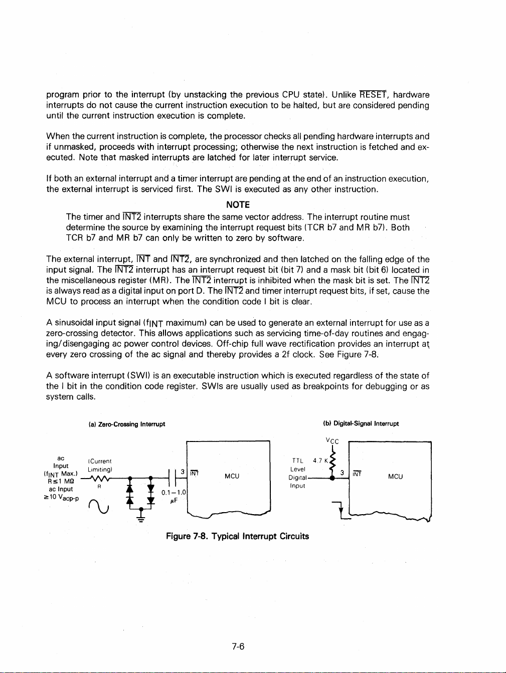
program prior to the interrupt (by unstacking the previous
interrupts do not cause the current instruction execution to
is
until the current instruction execution
complete.
CPU
state). Unlike
be
halted, but
li'ESEf,
are
considered pending
hardware
When the current instruction
if unmasked, proceeds with interrupt processing; otherwise the next instruction
is
complete, the processor checks
all
pending hardware interrupts and
is
ecuted. Note that masked interrupts are latched for later interrupt service.
If both
an
external interrupt and a timer interrupt are pending at the end
the external interrupt
is
serviced first. The SWI
is
executed
as
of
an
instruction execution,
any other instruction.
NOTE
The timer and INT2 interrupts share the same vector address. The interrupt routine must
(TCR
b7
determine the source by examining the interrupt request bits
TCR
b7
and
MR
b7
can
only
be
written to zero by software.
TNT
and
fI\JT2,
The external interrupt,
signal. The INT2 interrupt
input
the miscellaneous register (MRl. The INT2 interrupt
is
always
read
as
a digital input on port
MCU to process
an
interrupt when the condition code I bit
A sinusoidal input signal (fINT maximum)
zero-crossing detector. This
ing/
disengaging
ac
power control devices. Off-chip full wave rectification provides
every zero crossing of the
A software interrupt
I bit
in
the
the condition code register. SWls
(SWI)
allows applications such
ac
signal and thereby provides a 2f clock.
is
an
are synchronized and then latched
has
an
interrupt request bit (bit
is
D.
The
fI\IT2
and timer interrupt request bits, if set, cause the
can
be
used
as
executable instruction which
are
usually
7)
and a
inhibited when the mask bit
is
clear.
to generate
an
servicing time-of-day routines
is
executed regardless
used
as
breakpoints for debugging or
and M R
on
the falling edge of the
mask
bit (bit
external interrupt for
See
Figure 7-8.
system calls.
(a)
Zero-Crossing Interrupt
(b) Digital-Signal Interrupt
Vcc
fetched and
b7).
Both
6)
located
is
set. The INT2
use
and
engag-
an
interrupt
of
the state of
ex-
as
in
a
a~
as
ac
Input
(tINT Max.l ---'\Af'v---..-
Rs1
ac Input
~10
ICurrent
MO
Vacp-p
.....
---I
Figure
7-8.
MCU
Typical
7-6
Interrupt
4.7 K
TTL
Level 3
Digilal--
Input
Circuits
.....
--I
lJ
iNf
MCU
Page 49

SECTION 8
INPUT/OUTPUT CIRCUITRY
ANALOG-TO-DIGITAL CONVERTER
8.1
INPUT/OUTPUT CIRCUITRY
There
are
32
input/
output pins. The INT pin may
additional input pin. All pins
under software
is
accomplished by writing the corresponding bit
ing
logic zero for input.
control of the corresponding data direction register (DDR)' The port
On
input mode. The port output registers
reset
on
ports A,
all
the DDRs
B,
are
are
ware before changing the DDRs from input to output. A
an
output will
to
due
Internal
Connections
read
the contents of the output latch regardless of
output loading. Refer to Figure 8-1.
be
polled with branch instructions
and C
are
in
initialized
not initialized
AND
to
programmable
the port
to
a logic zero state, placing the ports
on
reset and should
read
operation
as
either inputs or outputs
I/O
DDR
to a logic one for output or a
be
initialized by soft-
on
a port programmed
the
logic levels at the output pin,
provide
an
programm-
in
the
as
* DDR
* * Port
Band
See SECTION
is
a write-only register and reads
C are three-state ports. Port A
11
ELECTRICAL CHARACTERISTICS.
Figu
as
all ones.
has
optional internal pullup devices to provide CMOS data drive capability.
re
8-1. Typical Port
8-1
I/O
Data
Direction
Register
Bit
,
,
0
Circu itry
Latched
Output
Data
Bit
0
,
X
Output
State MCU
0
, ,
Hi~Z*
Input
*
To
0
Pin
Page 50

All
inputloutput
patible
as
port
B,
C,
corresponding DDR. When programmed
lines
are
TTL compatible
as
both inputs and outputs. Port A lines
are
outputs (mask option on the MC6805R2, MC6805U2, MC6805R3, and MC6805U3) while
and 0 lines are CMOS compatible
as
inputs. Port 0 lines are input only; thus, there
as
outputs, port b
is
capable of sinking
10
and sourcing 1 milliampere on each pin.
0 provides the reference voltage, INT2, and multiplexed analog inputs for the MC6805R2,
Port
MC6805R3, MC68705R3,
puts. Port
VRH
and
VRl
and
PD5)
and
VRl
are
VRH
0 may always
are connected to the appropriate reference voltages.
internally connected
recommended input voltage range.
and MC68705R5. All
be
used
as
digital inputs and may also
to
the
AID
of
these lines
are
shared with the port 0 digital in-
be
used
TheVRl
resistor. Analog inputs may
as
analog inputs providing
and VRH lines (PD4
be
prescaled to attain the
CMOS com-
is
no
milliamperes
The address maps
register configuration
in
Section 3 give the addresses
is
provided
tions.
The corresponding DDRs for ports A,
$005,
and
are read-modfiy-write
"unaffected"
using a
PA7
PA6
PA5
PA2
PAl
PAO
PB7
PB6
PB5
PB3
PB2
PBl
PBO
single-store instruction.
40
Port A, bit 7
put. Bit 7 driving
driving
output option.
10mA
~.
~10mA
Port B, bit 0
put, driving
$006), A read
bits would
(CMOS Loads)
(1
TTL Load)
one
.--~.....--+
operation on these registers
in
function, they cannot
be
and
bit 4 programmed
CMOS loads and bit 4
TTL load directly using CMOS
and
bit 1 programmed
LEOs
directly.
of
data registers and data direction registers. The
in
Figure 7-6. Figure 8-2 provides some examples
CAUTION
B,
and C are write-only registers (registers at
is
undefined. Since BSET and
be
used
to
set or clear a single
set).
It
is
recommended that
PB7
32
PB6
31
PB5
30
PB4
29
PB3
28
PB2
27
as
out-
PBl
26
PBO
25
16
out-
PC7
PC6
PC5
PC4
PC3
PC2
PCl
PCO
15
14
13
12
11
10
9
V
as
all
DDR
bits
-'Ib
1.0
mA
~""'''''''JV'''''--'
Port
B,
bit 5 programmed
ing Darlington-base directly.
Port
C,
bits
0-3
programmed
CMOS loads, using external
driving
pullup resistors.
of
port connec-
DDR
bit (all
in
a port
be
written
2N6386 (Typical)
as
output, driv-
CMOS Inverter
MCl4049/MCl4069
(Typical)
as
output,
$004,
BClR
Figure 8-2a. Typical Port
Connections-
8-2
Output Modes
Page 51

SN74LS04 (Typical)
TTL driving port A directly.
PA7
PA6
38 PA5
PA4
37
PA3
36
PA2
35
PAl
PAO
SN74LS04
(Typical)
PB7
PB6
or MCl4069 •
CMOS or TTL driving port B directly.
PB5
29
PB4
28
PB3
27
PB2
PBl
PBO
PC7
15
PC6
14
PC5
13
PC4
12
PC3
11
PC2·
PCl
PCO
Port D
used
as
4-channel
as
CMOS digital input.
and MC68705R5
CMOS and TTL driving port C directly.
bit 7 used
MC6805R2, MC6805R3,
MC6805R3,
only.
Figure 8-2b. Typical Port Connections-Input Modes
The latched output data bit
all
of
writes
data register
its data bits
and
avoid undefined outputs; however,
modify-write instructions, since the data
(zero) and corresponds to the
8.2
ANALOG-TO-DIGITAL CONVERTER
(see
Figure
8-1)
must always
even
though the port
read
latched output data when the
be
written. Therefore, any write to a port
DDR
is
set to input. This may
care
must
corresponds to the pin
DDR
be
be
exercised when using
level
if the
is
an
output (onel.
The MC6805R2, MC6805R3, MC68705R3 and MC68705R5 microcomputers have
digital
(AI
D)
converter implemented
shown
in
Figure 8-3. Up
to
four external analog inputs,
through a multiplexer. Four internal analog channels may
(VRH-VRL VRH-VRL/2, VRH-VRL/4, and
on
the chip using a successive approximation technique,
via
port
0,
are
connected
be
selected for calibration purposes
VRU· The accuracy of these internal channels will not
necessarily meet the accuracy specifications of the external channels.
PDO/ANO
PD1/ANl
PD2/AN2
22
21
PD3/AN3
20
19
VRH
PD6/1NT2
18
PD7
AID
used
to initialize the
DDR
an
8-bitanalog-to-
to
VRL
input with
is
an
input
the
read-
as
AID
The multiplexer selection
8-1. This register
is
cleared during any reset condition. Refer
tion.
is
controlled
by
the
AID
control register (ACR) bits
to
Figure 7-6 for the register configura-
8-3
0,
1,
and
2;
see
Table
Page 52

D/A
15
kO
(Typ)
Control
Logic
Count
PDQ/ANO
PD1/ANl
PD2/AN2
PD3/AN3
Whenever the
(ACR bit
7)
is
1-of-8
Select
Multiplexer
AID
Control Register
ACR1
ACR2
0
0
0
0
1
1
1
1
* Internal (Calibration) Levels
ACR
is
written, the conversion
cleared,
and
the selected input
Figure
8-3.
AI
D
Table
8-1.
AI
D
Input
ACRO
0 0
0
1 0 AN2
1 1 AN3
0 0
0 1
1
1 1
Input Selected
1 AN1
0
ANO
VRH*
VRL*
VRH/4*
VRH/2*
in
is
sampled for five machine cycles and held internally.
progress
I.-
.....
Block
--.L_"--'---'-_"-
Diagram
MUX
Selection
AI
D Output (Hex)
Typ
Min
FE
FF FF
00
00
3F
40
7F
80
is
aborted, the conversion complete flag
During these five cycles, the analog input will appear approximately like a
capacitor
(plus approximately
Refer to Figure
8-4.
10
pF
for packaging) charging through a 2.6 kilohm resistor (typical).
8
AID
Result
.....
--'
Register
Max
01
41
81
25
picofarad (maximum)
The converter operates continuously using
sampled analog input. When the conversion
placed
in
the
AID
result register (ARR), the conversion complete flag
sampled again, and a new conversion
TheA/D
port D pins. An input
VRL converts to
is
imum
analog input should
is
ratiometric. Two reference voltages (VRH and VRU
$00.
provided. Similarly,
and
minimum ratings must not
voltage equal
An input voltage greater than
an
input voltage
use
VRH
as
is
started.
to
VRH
converts to
less
than VRL, but greater than VSS converts to
be
exceeded. For ratiometric conversion, the source
the supply voltage and
30
machine cycles to complete a conversion
is
complete, the digitized sample
is
are
$FF
VRH
(full
converts to
be
referenced to VRL. To maintain the full
supplied to the converter via
scale)
and
$FF
and no overflow indication
of
set, the selected input
an
input voltage equal
8-4
of
digital value
$00.
Max-
of
each
the
is
is
to
Page 53

Figure
8-4.
Device
Analog
Input
Effective
Channel
Select
Analog
Input
Inpedance
(During
Sampling
Only)
accuracy on the
than
VSS but
than 4
volts.
The
AI
D
±
Y2
LSB, rather than +
point from
Y2
LSB below VRH, ideally. Refer
1
On
release
be
selected and the conversion complete flag will
Converter
Output
(Hex)
has
$00
of
AID,
VRH
should
be
equal to or
less
than the maximum specification and (VRH-VRU should
a built-in
to
reset, the
$01
Y2
LS
B offset intended to reduce the magnitude
a,
-1
LSB
occurs at
AID
Y2
LSB above VRL. Similarly, the transition from
control register (ACR)
with
no offset. This implies that, ignoring errors, the transition
to
Figures 8-5 and 8-6.
FF
FE
FD
FC
FB
FA
F9
F8
08
07
06
05
04
03
02
01
00
1x
2x
vRL
3x 4x
5x
x=_1_*(VRH-VRL)=1
6x
256
less
than VDD, VRL should
is
cleared therefore after reset, channel
be
clear.
Error Convention
±2
LSBs
250x
251x 252x 253x 254x 255x vRH
LSB
be
equal to or greater
be
equal to or greater
of
the quantizing error to
$FE
to
$FF
occurs
zero
will
Figure
8-5.
Ideal
Converter
8-5
Transfer
Characteristic
Page 54

Digital
Output
Offset
(Positive)
Digital
Output
FF
FF
00
K..
,/
,/
________
(a)
Offset Error
,/,/\
/ Ideal
,/
(b) Full
,/
Scale
,/
,/
,/
,/
Analog Input
Error
...,.
__
~~
Analog Input
Full
Scale
Error
(e)
Non-Linearity
Digital
Output
FF
- - - - - -
00 Analog Input
Non-
Linearity
Figure 8-6. Types
(VRH-1
of
Conversion Errors
8-6
LSB)
Page 55

SECTION 9
MASK
The
information in this section pertains only to the MC68705R3, MC68705U3, MC68705R5, and
MC68705U5 EPROM versions
9.1
MASK OPTIONS
The MC68705R3, MC68705U3, MC68705R5, and MC68705U5 mask option registers are im-
in
plemented
ing (if erased),
When used
junction
b3
is the secure/non-secure mode option
MC68705R3/MC68705U3), and b4 is
the
timer prescaler. Bit
grammed
If
the MOR timer option (TOPT) bit is a zero, the MC6805R3 and MC6805U3 are emulated. Here,
bits
b5,
zation the
EPROM. Like
to
emulate the MC6805R2 and MC6805U2, five
with
the prescaler. Of the remaining, the
b6
determines the timer option selection. The value
to
configure the TCR
b4, b2, b1, and
TCR
bO
is
software controllable.
OPTIONS AND PROGRAMMING
of
the M6805 Family.
all
other EPROM bytes, the MOR contains all zeros prior
of
the eight MOR bits are used
b7
bit
is
used
to
select the type
for
the MC68705R5/MC68705U5 only (b3
not
(a
logic one
set the initial value
used. Bits
for
of
bO,
b1, and
MC6805R2/ MC6805U2 emulation!.
their respective TCR bits during reset.
b2
determine the division
of
the TOPT
to
programm-
in
of
clock oscillator,
is
not
used by
bit
(b6)
After
con-
of
the
is
pro-
initiali-
A description
b7,
ClK
TOPT Timer Option
b6,
of
r--:;.;b
1.....1
_c_lK--1...1
* MC68705R5 and MC68705U5 only.
Clock Oscillator Type
=
RC
1
0=
Crystal
VIHTP on the TIMER (pin
1 =
MC6805R2/MC6805U2type timer/prescaler. All bits, except
control register
option register determine the equivalent
0=
MC6805R3/MC6805U3 type timer/prescaler. All TCR bits are implemented
ware programmable
values
tion).
the MOR bits
7---,~b;;..;;6--r--..;;b;.;;.5-.,-~b4~,--..;;;.b3~r--b;;;.;;2;;......,---..;b;...;1--.,.--..;;b:...:.0--,M
T_o_p_T-LI_c_l_s-'-I_---II_s_N.-;.M_*
is
as
follows:
ask Option
lL..---p_2-J..._P_1-..L._P0-.lIRegister
$F38
NOTE
8)
forces the crystal mode.
b6
(TCR) are invisible
timer, The state
of
their respective TCR bits (TCR
and b7,
to
the user. Bits b5, b2,
MC6805R2/ MC6805U2 mask optio.ns.
of
bits
b5,b4,
is
then software controlled after initializa-
b2,
b1,
b1,
and
and
of
the timer
bO
of
the mask
as
bO
set the initial
a soft-
9-1
Page 56

b5,
CLS
Timerl Prescaler Clock Source
1 = External
0=
Intenal phase two.
TIMER pin.
b4
b3,
b2,
b1,
bO,
Two examples for programming the
Example 1
Not used if
TIE
SNM* When this bit
contents
9.4 PROGRAMMING FIRMWARE.
Note, For MC68705R3
P2
Prescaler
P1
puts
PO
combinations of these three bits.
P2
0
0
0 1
0
1
1
1 1 0
1
To emulate
event count input for the timer with no prescaling, the
11110000.
byte.
MOR
TOPT = 1 (MC6805R2/MC6805U2 emulationl. Sets initial value
if
MOR
TOPT=O (MC6805R3/MC6805U3 emulationl.
is
set, i.e., programmed to a one, it
of
the MC68705R5 and MC68705U5 externally. For more information refer to
and
MC68705U3 operation,
Option - the logic levels
on
the timer prescaler. The table below shows the division resulting from decoding
Pl
PO
Prescaler
0 0
0
1
0
0
1
an
MC6805R2/MC6805U2 to verify your program with
To write the
1 (Bypass Prescaler)
1
2
0 4
1
8
0
16
1
32
64
1
128
mask
mask
option register, it
of
these bits, when decoded, select one
Division
option register
is
not possible to access the
b3
is
not used.
are
discussed below.
mask
option register would
is
simply programmed
an
RC
as
of
eight out-
oscillator and
be
any other
of
TCR
EPROM
an
set to
EPROM
Example 2
use
Suppose you wish to
tion), and you wish the initial condition
an
abled and
mask
option register would
9.2 ON-CHIP PROGRAMMING HARDWARE
The programming control register
least significant bits (the five most significant bits
*MC68705R5
internal clock source. If the clock oscillator was to
and
MC68705U5 only.
programmable prescaler functions (MC6805R3/MC6805U3 emula-
of
the prescaler to
be
set to
00000110.
(PCR)
at location
9-2
$OOB
are
be
divided by
is
an
8-bit register which utilizes the three
set
to
logic ones). This register provides the
64,
with the input dis-
be
in
the crystal mode, the
Page 57

necessary control bits
PCR
when programming
description
of
each
bit follows.
b7
bO,
PIE
Programming Latch Enable - When cleared, this bit allows the address and data to
latched into the EPROM. When this bit
1 = (set)
0=
(clear) latch address and data into
PLE
is
set during a reset, but may
b1,
J5GE
b2,
VPON (Vpp
EPROM
Program Enable - When cleared,
only
i.e., setting up the byte
PGE
one.
voltage"
VPON being one "disconnects"
dental clearing
is
be
cleared if PIT
1 = (set) inhibit
0=
(clear) enable
is
set during a reset; however, it
ON)
1 = no
0=
"high
VPON being zero does not indicate that the
programming.
normal operating mode.
to
allow programming the EPROM. The bootstrap program manipulates the
so
that users
b6 b5
read
EPROM
inhibited if VPON
- VPON
is
present at the
"high
voltage" on
voltage" on
of
these bits from affecting the normal operating mode .
need
not
be
concerned
b4
b3
b2
I VPON I
is
be
cleared any time. However, its effect on the
is
a logic one.
f5GE
enables programming
is
cleared.
to
EPROM
EPROM
is
a read-only bit and when at a logic zero it indicates that a
It
is
PGE
be
programmed.
programming
programming (if
Vpp
pin.
Vpp
Vpp
pin
PGE
used
as
a safety interlock for the user
must
has
pin
and
. NOTE
no effect on
PLE
with
the
PCR
in
most applications. A
b1
bO
Programming
PGE I PLE
set, data can
EPROM
be
(read disable)
set when changing the address and data;
PIE
is
from the rest
Vpp
level
be
low)
EPROM
of
is
IControl
Register $008
read
from the EPROM.
of
the EPROM.
circuits if VPON
the chip, preventing acci-
correct for
in
the
PGE
is
a logic
be
can
"high
The programming
VPON
PGE
a a a Programming mode (program
1 a
control register functions
PLE
o
PG
Programming Conditions
E and
PLE
disabled from system
are
shown below.
EPROM
a 1 a Programming disabled (latch address and data
1 1
a a
1 a 1 Invalid state; PGE=O
a
1
a
PG
E and
'PIE
disabled from system
1 Invalid state; PGE=O iff
iff
1
"High
voltage" on
1
PGE
and
PLE
Vpp
disabled from system (operating mode)
PIT
= a
PIT = a
9-3
byte)
in
EPROM)
Page 58

9.3 ERASING THE EPROM
The
EPROM
2537
lamps should
The
one inch from the UV tubes.
is
the entered by programming ones into the desired bit locations.
tects both the
9.4 PROGRAMMING FIRMWARE
The MC68705R3, MC68705U3, MC68705R5, and MC68705U5 have
taining a bootstrap program which
$FF6
to pin 8 (TIMER pin) and the
schematic diagram
the
EPROM.
tents
erasing the entire
9.5 PROGRAMMING STEPS
The MCM2532 UV
that
EPROM
or MC68705U5 and the MCM2532
mounted in sockets.
can
be
erased by exposure
to
high-intensity ultraviolet (UV) light with a wavelength
angstroms. The recommended integrated dose (UV intensity x exposure time)
be
used
without
Be
sure that the
EPROM
EPROM
and
$FF7
is
used to start executing the program. This vector
of
a circuit and a summary
It
is
possible to program the
in
the secure mode. The only way to go from the secure mode to the non-secure mode
shortwave filters and the
Ultraviolet erasure clears all bits
CAUTION
window
is
shielded from light except when erasing. This pro-
and light-sensitive nodes.
can
be
used to program the EPROM. The vector at addresses
RESET
pin
is
allowed to rise above
of
programming steps which
EPROM
via
the bootstrap software and validate its con-
EPROM
of
should
the
EPROM
120
bytes
is
fetched when VIHTP
VIRES
be
to the zero state. Data
of
+.
Figure
can
be
EPROM.
EPROM
is
to
be
transferred to the MC68705R3, MC68705U3, MC68705R5, or MC68705U5. Non-
must first
be
programmed
with
an
exact duplicate
of
addresses are ignored by the bootstrap. Since the MC68705R3, MC68705U3, MC68705R5,
are
to
be
inserted and removed from the circuit, they should
In
Be
sure
S1
addition, the precaution below must
CAUTION
and
S2
are closed and
VCC
and +
26 V are
be
observed (refer to Figure 9-1).
not applied when inserting the
MC68705R3, MC68705U3, MC68705R5, or MC68705U5 and MCM2532 into their respective sockets. This ensures that
RESET
is
held
low
while inserting the devices.
of
Ws/cm
2
is
25
positioned about
mask
ROM
con-
is
applied
9-1
provides a
used
to
program
is
by
the information
be
.
When ready to program the
necessary to provide
S1
(to remove reset). Once the voltages
put
control line
PB3
output (COUNT), The counter selects the MCM2532
equivalent
COUNT
EPROM
clocks the counter to the next
VCC
(PB4)
goes high and then low, then the 12-bit counter (MC14040B)
byte selected by the bootstrap program. Once the
MC68705R3, MC68705U3, MC68705R5, or MC68705U5 it
and
+26
volts, open switch
are
applied and both
EPROM
S2
(to apply Vpp and VIHTP), and then open
location. This continues until the
pletely programmed at which time the programmed indicator
the
loop
is
repeated to verify the programmed data. The verified indicator
ming
is
correct.
9-4
S2
and
EPROM
LED
is
S1
are open, the
is
byte which
EPROM
location
EPROM
lit. The counter
LED
lights if the program-
is
only
CLEAR
outclocked by the
is
to load the
is
loaded,
is
com-
is
cleared and
Page 59

co
U,
RESET
2
-
®.
'CC'"
r
4.7 k
1 V
I~
~'
~
~
11\111711')/\
Summary
~
1.
2.
3.
o 1
-L.-
. T
:::~
0.1
lN4001 1.0 a
~
100
{}
4.7 k J 2N2222
@
~
+12
V
~
~~
TO.Ol
...,,..
of
Programming Steps:
When plugging in the MC68705R3, MC68705U3, MC68705R5, or MC68705U5 or the MCM2532
and that V
CC
To initiate programming, be sure
Before removing the MC68705R3, MC68705U3, MC68705R5, or MC68705U5, first close
26
V then remove the MC68705R3, MC68705U3, MC68705R5, or MC68705U5.
+
*'0
100.1
PFT
~,MH~
~"-
I1
':"
75
:~1
':"
VIHTP
2N2222
~
~
1N4001
~
1N4001
4.7 k
~
CC
and +
26
V are
RESET
,
VSS
L
INT
4
Vce
_ 5
EXTAl
XTAl
pF
7
VPP
8 TIMER
25
PBO
26
Programmed
not
applied.
Sl
PB1
//
~.
~
> 470
is
closed,
L!)
::>
L!)
0
r--
~
u
~
0
L!)'
a::
L!)
0
r--
~
u
~
c.,.;
::>
L!)
0
r--
~
u
~
a::
L!)
'"
0
r--
~
u
~
PA5
PA4
PA2
PAO
PB2
27
....
~
~
S2
PA7
PA6
PA3
PAl
PB4
PB3
II
Verified
470
is
closed and
40
39
38
37
36
35
34
33
Vec
29
28
Vce~
Jl
0.1
I
':"
VCC
and +
18
E/All
~
0
a::
0...
w
:><::
("'oJ
~
("'oJ
C'?
L!)
("'oJ
~
u
~
AlO
A9
A8
A7
A6
A5
A4
A3
A2
Al
AO
G
20
19
22
23
1
2
3 2
4
5
6 6
8 9
---u-u-u-
Vpp
17
07
16
06
15
05
14
04
13
03
11
02
10
Dl
9 7 7
DO
24
Vee
Vss
12
~
1
15
14
12
13
4
3
5
CLEAR
COUNT
-::
VCC=
+5.0
VSS=O.OV
Vpp=21.0
25
V are applied. Then open S2, followed by
V (typical)
V ± 1.0 V (Programming Mode)
be
sure that
S2
and then close
Sl.
012
011
010
09
Qj
§
08
0
u
07
~
N
06
-
III
3
05
~
u
04
~
03
02
01
~--
Sl
and
Disconnect
16
VDO
Vss
~
elK
RST
-
S2
are closed
Sl.
Vce
V
e
lo
10
11
-""
-""
.
".
~
.
"
.i
......-
V~C
and
Figure
9-1.
Programming
Connections
Schematic
Diagram
Page 60

Once the
and close switch
socket.
EPROM
has
been programmed and verified, close switch
S1
(to reset). Disconnect
+26
volts and VCC, then remove the
S2
(to remove
Vpp
and VIHTP)
EPROM
from its
9.6 EMULATION
The MC68705R3 and MC68705R5 emulate the MC6805R2 and MC6805R3 while the MC68705U3
and MC68705U5 emulate the MC685U2 and MC6805U3
MC6805R3,
EPROM
below.
1.
2.
3.
and MC6805U3 mask features are implemented
byte. There are a few minor exceptions to the exactness
The
MC6805R21
mented
must
MC6805R3/MC6805U3. (The MC6805R2/MC6805U2 and MC6805R3/MC6805U3
zeros from this area.)
The reserved
change
reserved
and MC68705U5 use this
The MC6805R2/MC6805U2 and MC6805R3/MC6805U3
RAM"
MC6805R3/MC6805U3 mask
(M
in
be
without
ROM
area.
C68705R31
MC6805U2 and
the MC68705R3/MC68705U3 and MC68705R5/MC68705U5 and these
left unprogrammed to accurately simulate the MC6805R2/MC6805U2 and
ROM
areas
notice. The MC6805R2, MC6805U2, MC6805R3, and MC6805U3
for the self-check feature while the MC68705R3, MC68705U3, MC68705R5,
area
This RAM
M
C68705U3
MC6805R31
have different data stored
for the bootstrap program.
is
not implemented
ROM
version, but
and M
C68705R51
MC6805U3
M
"exactly."
in
in
read
in
is
implemented
C68705U5)
MC6805R2, MC6805U2,
the mask option register (MOR)
of
emulation which are listed
"future
them and this data
the MC6805R2/MC6805U2 and
.
all
ones
ROM"
in
their
in
the
areas
is
48
byte
EPROM
are imple1728
bytes
read
all
subject to
use
the
"future
version
4.
The
Vpp
line (pin
versions
MC6805R3/MC6805U3 mask
5.
The
6.
The MC68705R3/MC68705U3 and MC68705R5/MC68705U5
tion
on the MC6805R2/MC6805U2 and MC6805R3/MC6805U3 mask
pin 7
The operation
same way
is
LVI
feature
in
the MEX6805 Support System.
as
previously noted.
of
all
in
all
devices including interrupts, timer, data ports, and data direction registers (DDRs).
7)
in
the MC68705R3/MC68705U3 and MC68705R5/MC68705U5
tied to
other circuitry
VCC
is
not available
for normal operation.
ROM
versions, pin 7
in
the
has
EPROM
In
been
exactly duplicated or designed to function exactly the
version.
normal operation, all pin functions
9-6
In
the MC6805R2/MC6805U2 and
is
grounded
in
normal operation.
EPROM
versions do not func-
ROM
versions, except for
are
EPROM
the same
as
Page 61

SECTION
10
SOFTWARE
10.1
BIT MANIPULATION
The microcomputers have the ability to set or clear any single RAM or
BCLR)
(see
tion registers) with a single instruction (BSET,
can
be
tested using the
state. The carry bit equals the
working with any bit
handle single
The corresponding data direction registers for ports A,
(locations
BSET
tion regiser bit
tion register bits
and
liD
$004,
BCLR
BRSET
in
bits
as
$005,
are
(all
"unaffected" bits would
in
and
BRCLR
value of the bit references by BRSET or BRCLR. The capability of
RAM, ROM, or
control lines.
and
$006), A read
read-modify-write functions, they cannot
a port
be
written using a single-store instruction.
instructions
liD
allows the user to have individual flags
CAUTION
operation
be
set). It
Caution below). Any bit
and
the program branches
B,
and C are
on
these registers
be
is
recommended that
liD
bit (except the data direc-
in
as
a result of its
in
RAM or to
write-only registers
is
undefined. Since
used
to set a data direc-
all
data direc-
page
zero
The coding examples shown
instruction. Assume that the microcomputer
has
external device
time, least significant bit first out
clocks the external device, picks up the data
accumulates the data bit
Device
a data ready signal, a data output line, and a clock line to clock data one bit at a
READY
Serial
Clock
Data
in
Figure
10-1
illustrate the usefulness of the bit manipulation
of
the device. The microcomputer waits until the data
in
a random-access memory location.
I---
2 p
,
OA
~
T
MCU
-
Figure
10-1.
Bit
is
to
communicate
in
the carry flag, clears the clock line, and finally
Manipulation
10-1
with
SELF
CONT
Examples
an
external serial device. The
BRSET
BSET 1 ,PORTA
BRCLR
BCLR
ROR
2,PORTA,SELF
O,PORTA,CONT
I,PORTA
RAMLOC
and
is
test
ready,
Page 62

10.2 ADDRESSING MODES
The microcomputers have ten addressing modes available for
plained briefly
M6805 HMOSIM146805 CMOS Family Microcomputer/Microprocessor User's Manual.
in
the following paragraphs. For additional details
use
by the programmer. They
and
illustrations, refer to the
are
ex-
The term
address from which the argument for
10.2.1
In
opcode. The immediate addressing mode
program execution
10.2.2 Direct
In
following the opcode byte. Direct addressing allows the user to directly address the lowest
bytes
I/O
10.2.3 Extended
In
bytes following the opcode. Instructions with extended addressing modes
ing arguments anywhere
assembler,
The
10.2.4 Relative
The relative addressing mode
tents of the 8-bit signed byte (the offset)
branch condition
addressing
calculating the correct offset if
and checks
"effective address"
Immediate
the immediate addressing mode, the operand
(e.
the direct addressing mode, the effective address of the argument
in
memory with a single two-byte instruction. This address
registers
the extended addressing mode, the effective address of the argument
assembler automatically selects the shortest form of the instruction.
and
128
the user
is
from
to
see
bytes of
need
is
true. Otherwise, control proceeds to the next instruction. The
-126
if it
(EA)
is
used
in
describing the addressing modes.
an
instruction
is
used
g., a constant
in
memory with a single three-byte instruction. When using the Motorola
·not specify whether
to + 129
is
within the span of the branch.
used
to initialize a loop counter).
ROM.
Direct addressing
is
only
used
in
following the opcode
from the opcode address. The programmer
he
uses
the Motorola assembler, since it calculates the proper offset
is
fetched or stored.
is
contained
to access constants which do not change during
an
instruction
branch instructions.
is
in
the byte immediately following the
is
area
includes
an
effective
use
uses
direct or extended addressing.
In
relative addressing, the con-
is
added to the
EA
is
defined
contained
of both memory
is
are
in
a single byte
all
on-chip
contained
capable of referenc-
PC
if, and only if, the
span
need
not worry about
RAM
and
in
of
as
the
relative
the
256
and
time.
two
10.2.5 Indexed, No Offset
In
the indexed, no offset addressing mode, the effective address of the argument
can
8-bit index register. Thus, this addressing mode
are
only
on
instructions
hold the address of a frequently referenced RAM or
10.2.6 Indexed,
In
the indexed, 8-bit offset addressing mode, the effective address
unsigned 8-bit index register and the unsigned byte
byte long. This mode
8-Bit Offset
access the first
is
often
used
I/O
location.
following the opcode. This addressing mode
to move a pointer through a table or to
256
memory locations. These
is
the sum of the contents of the
10-2
is
contained
in
the
is
Page 63

useful
in
selecting the kth element
typically
may begin anywhere within the first
510
10.2.7 Index, 16-Bit Offset
In
the unsigned 8-bit index register and the
mode
allows tables
shortest form
10.2.8 Bit Set/Clear
I
n the bit set/ clear addressing mode, the bit to
following the opcode specifies the direct addressing
or cleared. Thus, any read/write bit
selectively set or cleared with a single two-byte instruction.
10.2.9 Bit Test and Branch
The bit test and branch addressing mode
ing. The bit which
address
Signed
the specified memory location. This single three-byte instruction allows the program to branch
based on the condition
ching
to
be
in
X with the address
($1
FE
is
the last location at which the instruction may beginl.
the indexed, 16-bit offset addressing mode, the effective address
can
be
used
in
a manner similar to indexed, 8-bit offset except that this three-byte instruction
to
be
anywhere
of
indexed addressing.
The corresponding DDRs for ports A,
$005,
and
$006). A read
are
read-modify-write
"unaffected"
written using a single-store instruction.
of
the byte to
relative 8-bit offset
is
from
the carry bit
bits would
-125
of
the condition code registers.
in
is
to
be
be
tested
in
of
any readable bit
to +
130
in
an
n element table. With this two-byte instruction, k would
of
the beginning
256
addressable locations and could extend
two
in
memory. As
operation on these registers
function, they cannot
be
setl. It
tested and condition (set or
is
in
the third byte
from the opcode address. The state
with
in
the first
CAUTION
B,
is
recommended that
is
a combination
the single byte immediately following the opcode byte. The
is
in
of
the table
unsigned bytes following the opcode. This addressing
direct and extended, the Motorola determines the
be
set or cleared
of
the byte
256
locations
and C
are
write-only registers (registers at
is
undefined since BSET and
be
used to set or clear a single
of
direct addressing
clear)
added to the
the first
See
PC
256
locations
Caution under paragraph 10.2;8.
in
the instruction. As such, tables
as
far
as
location
is
the sum
is
part
of
in
which the specified bit
of
memory, including
all
DDR
bits
is
included
if the specified bit.is set or cleared
of
memory. The span of bran-
of
the tested bit
of
the contents
the opcode, and the byte
is
to
be
I/O,
can
$004,
BCLR
DDR
bit
(all
in
a port must
and
relative address-
in
the opcode, and the
is
also transferred
be
of
set
be
in
10.2.10 Inherent
In
the inherent addressing mode,
tained
in
the opcode. Operations specifying only the index register or accumulator,
trol instruction with no other agruments, are included
long.
10.3 INSTRUCTION SET
The MCU
produce
write, branch, bit manipulation, and
the instructions within a given type are presented
has
a set
of
59
207
usable opcodes. They
basic instructions, which when combined
all
the information necessary to execute the instruction
can
be
divided into five types: register/memory, read-modify-
control. The following paragraphs briefly explain
in
10-3
is
as
well
as
in
this mode. These instructions are one byte
with
the
10
addressing modes
each
type. All
individual tables.
concon-
Page 64

10.3.1 Register/Memory Instructions
Most of these instructions
register. The other operand
unconditional (JMP) and jump to subroutine
10-1.
Table
use
two
operands.
is
obtained from meory using one
One
operand
(JSR) instructions have no register operand. Refer to
is
either the accumulator or the index
of
the addressing modes. The jump
10.3.2 Read-Modify-Write Instructions
These instructions
modified value back to memory or to the register
negative or zero
not perform the write. Refer to Table
read
a memory location or a register, modify or test its contents, and write the
(see
Caution under paragraph 10.2.8). The test for
(TST) instructions is included
in
the read-modify-write instructions, though it does
10-2.
10.3.3 Branch Instructions
The branch instructions cause a branch from the program when a certain condition
10-3.
Table
is
met. Refer to
10.3.4 Bit Manipulation Instructions
These instructions
paragraph
10.2.8.
operations. Refer to Table
are
used
on
any bit
One
group either sets or clears. The other group performs the bit test and branch
in
the first
256
bytes of memory;
see
Caution under
10-4.
10.3.5 Control Instructions
The control instructions control the MCU operations during program execution. Refer to Table
10-5.
10.3.6 Alphabetical Listing
The complete instruction set
10.3.7 Opcode Map Summary
Table
10-7
is
an
opcode made for the instructions
is
given
in
alphabetical order
used
10-4
in
on
the MCU.
Table
10-6.
Page 65

Table
10-1.
Register
Memory
Instructions
~
o
0,
Function
Load A from Memory
Load X from Memory LOX AE
Store A
in
Store X
Add
Add
Subtract Memory
Subtract Memory
AND
OR
Exclusive
Arithmetic Compare A
Arithmetic Compare X
Bit
Jump
Jump
Memory
in
Memory STX
Memory
to
Memory and Carry
with
Memory
Memory
with
with
Test Memory
(Logical Compare) BIT
A
Borrow SBC A2 2 2
Memory CMP
Memory CPX
Unconditional
to
from
to
A
with
A ORA
OR
Memory
with
Subroutine JSR
to
A ADC
A
with
A
Mnemonic
A
Code
LDA
STA
ADD
SUB
AND
EOR
JMP
Immediate
Op
# #
Bytes
A6
- -
-
AB 2 2 BB 2
A9 2
AO
A4
AA
AS
A1
A3 2 2
A5 2 2
-
- - -
Cycles
2 2
2
- -
2
2 2
2 2
2 2
2 2
- -
2
-
2
2
Direct
Op
Code
Bytes
B6
BE
B7
BF
B9
BO
B2
B4
BA
BS
B1
B3
B5
Be 2 3
BD 2 7
# #
2 4
2 4
2 5
2 5
2
2
2 4
2 4
2 4 CA
2
2 4
2 4
2 4
Cycles
4
4
4
4
Op
Cqde
C6
CE
C7
CF
CB
C9
CO
C2
C4
CS
C1
C3
C5
CC
CD
Addressing
Extended
# #
Bytes
3 5
3 5
3 6
3 6
3
3
3
3
3
3
3 5
3
3 5
3 5
3 4
~
Modes
Indexed Indexed
(No
Offset)
Op
# #
Code
Cycles
-5
5
5
5
5
5 FA 1 4
5
S
-
F6
FE
F7
FF
FB
F9
FO
F2
F4
FS
F1
F3
F5
FC
FD
Bytes
1 4
1 4
1 5
1
1 4
1 4
1 4
1 4
1 4
1 4
1
1
1
1
1
Cycles
5
4
4
4
3
7
(8-Bit
Offset)
Op
# #
Bytes
Code
E6
EE
E7
EF
EB
E9
EO
E2
E4
EA
ES
E1
E3
E5
EC
~D
Cycles
2 5
2 5
2 6
2 6
2 5 DB
2 5 D9
2 5
2 5
2 5 D4
2 5
2 5
2 5
2 5 D3 3 6
2 5
2 4 DC
_
2_
,---S
__
Indexed
(16-Bit
Op
Code
D6
DE
D7
DF
DO
D2
DA
DS
D1
D5
~~--
'-~
Offset)
#
Bytes
3
3 6
3
3
3 6
3
3 6
3 6
3
3 6
3 6
3 6
3
3
#
Cycles
6
7
7
6
6
6
5
'------9_
Page 66

Function'
Increment
Decrement
Clear
Complement
Negate (2'8 Complement)
Rotate Left Thru Carry ROL
Rotate Right Thru Carry
Logical
Shift
Logical
Arithmetic
Test
Left LSL
Shift
Right
Shift
for
Right ASR
Negative or Zero TST
Mnemonic
INC 4C 1 4
DEC
CLR
COM
NEG
ROR
LSR
Table
10-2.
Inherent
# #
Op
Code
Bytes
1 4
4A
4F 1
43 1 4
40 1 4
49 1 4
46 1 4
48 1 4
1
44
47
1 4
40
1 4
Read-Modify-Write
Inherent
(A)
Cycles
4
4 54
Op
Code
5C
5A
5F
53
50
59
56
58
57
50
(X)
# #
Bytes
1 4
1 4
1
1 4
1 4 30 2 6
1 4
1
1 4
1 4
1
1
Cycles
4
4
4
4
Instructions
Addressing
Op
Code
3C
3A
3F
33
39
36
38
34
37
3D
Direct
# #
Bytes
2
2 6
2 6
2 6
2 6
2 6
2 6
2 6
2
2
Modes
Cycles
Indexed Indexed
(No
Offset)
Op
# #
Bytes
Code
7C
6
6
6
1 6 6C 2
7A
1 6
7F
1 6 6F 2
73
1 6
70
1 6
79 1 6
76
1 6
78 1 6 68
74
1 6
1
77
70
1 6
Cycles
6
(S-Bit
Op
Code
6A
63
60
69
66
64
67
60
Offset)
# #
Bytes
2
2
2
2
2
2
2
2 7
2
Cycles
7
7
7
7
7
7
7
7
7
7
Page 67
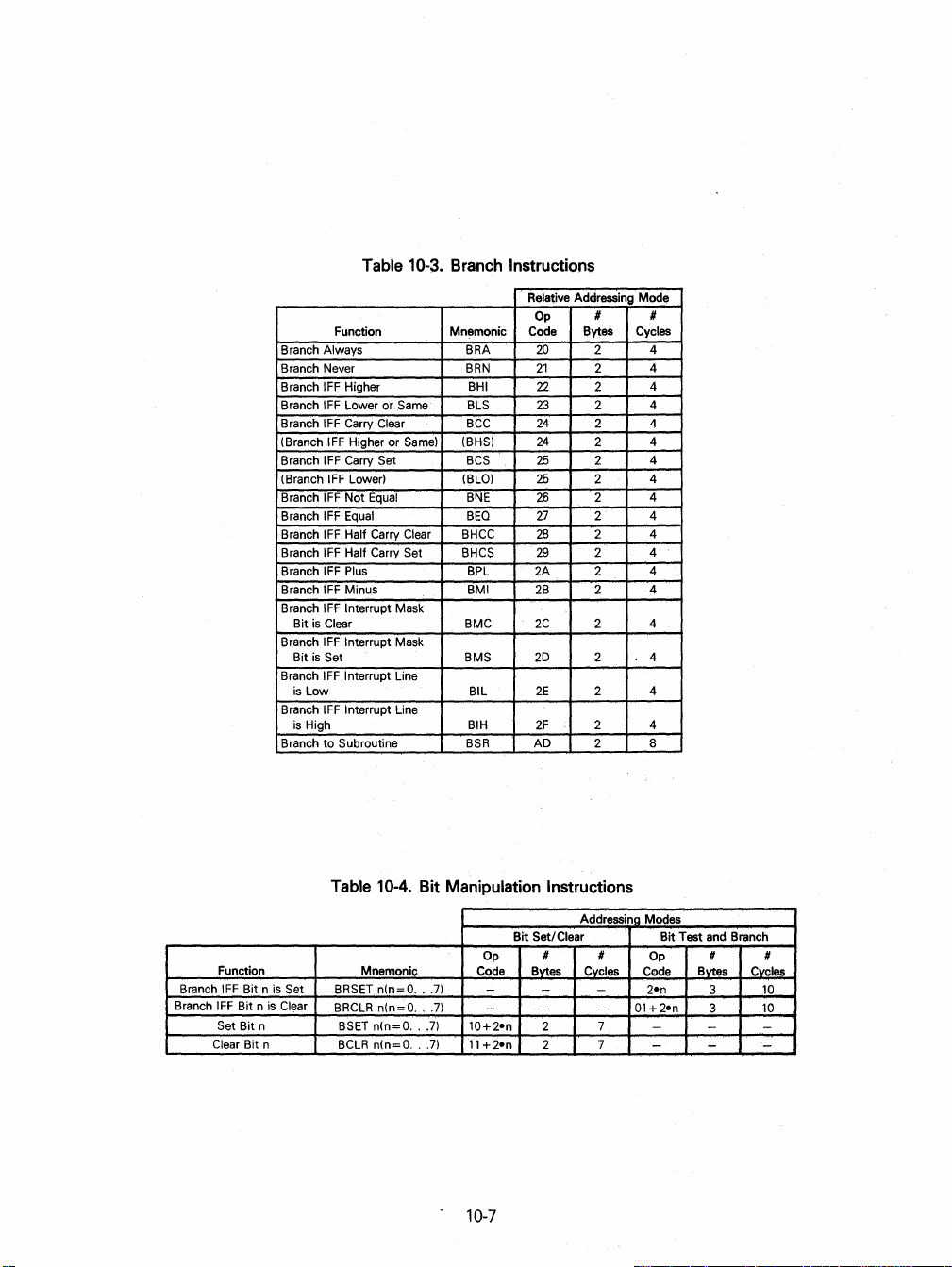
Table 10-3. Branch Instructions
Function
Branch Always BRA
Branch Never
IFF
Branch
Branch
Branch
(Branch
Branch
(Branch
Branch
Branch
Branch
Branch
Branch
Branch
Branch
Branch
Branch
Branch
Branch
Higher BHI
IFF
Lower or Same BLS
IFF
Carry Clear
IFF Higher or Same)
IFF
Carry Set
IFF
Lower)
IFF
Not
Equal
IFF
Equal
IFF
Half Carry Clear
IFF
Half Carry Set BHCS
IFF
Plus BPL 2A 2 4
IFF
Minus BMI
IFF
Interrupt Mask
is
Clear
Bit
IFF
Interrupt Mask
Bit
is
Set
IFF
Interrupt Line
is
Low
IFF
Interrupt Line
is
High
to
Subroutine
Mnemonic
BRN
BCC
(BHS)
BCS
(BLO)
BNE
BEQ
BHCC
BMC
BMS
BIL
BIH
BSR
Relative Addressing Mode
op
Code Bytes
20
21
22
23
24
24
25
25
26
27
28
29
2B
2C
2D
2E
2F
AD
#
Cycles
2
2
2
2
2
2
2
2
2
2 4
2
2
2
2
2
2
2
2 8
#
4
4
4
4
4
4
4
4
4
4
4
4
4
4
4
4
Branch
Branch
Function
IFF
Bit n is Set BRSET
IFF
Bit n is Clear
Set Bit n
Clear Bit n
Table 10-4. Bit Manipulation Instructions
Addressing Modes
Setl Clear Bit Test and Branch
# #
Cycles
-
-
-
-
7
2
7
2
Mnemonic
n(n=O
BRCLR
n(n=O
BSET n(n:;:O
BCLR
n(n=O
...
...
...
...
7)
7)
7)
7)
Bit
op
Code Bytes
-
-
10+2-n
11
+2-n
10-7
Code
01
op
2-n
+2-n
-
-
# #
Bytes
3
3
- -
-
Cycles
10
10
-
Page 68

Table
10-5.
Control Instructions
Function Mnemonic
Transfer A to X TAX
Transfer X to A TXA
Set Carry Bit
Clear
Carry Bit
Set Interrupt Mask Bit
Clear Interrupt Mask Bit
Software Interrupt SWI
Return from Subroutine
Return from Interrupt
Reset
Stack Pointer
No-Operation
Table
10-6.
SEC
CLC
SEI
CLI
RTS
RTI
RSP
NOP
Instruction Set (Sheet 1
Inherent
Op
Code
97
9F
99
98
9B
9A 1
83
81
80 1
9C
9D 1
# #
Bytes Cycles
1 2
1 2
1
2
1
2
1
2
2
1
11
1
6
9
1
2
2
of
2)
Inherent'
~Mneml
ADC
ADD
AND
ASL
ASR X
BCC
BCLR
BCS
BEQ
BHCC
BHCS
BHI
BHS
BIH
BIL
BIT
BLO
BLS
BMC
BMI
BMS
BNE
BPL
BRA
Condition Code
H Half Carry (From Bit
I Interrupt Mask
N Negative
Z Zero
X
Symbols:
(Sign Bit)
Immediate
X
X
X
X
3)
Direct
X
X
X
X
X
X
I
I
I
I
Addressing
Extended
C Carry/Borrow
/\
•
Relative
X X
X
X
X X
Test and Set if True, Cleared Otherwise
Not Affected
Modes
Indexed
(No
Offset)
X
X
X
X
X
X
X
X
X
X
X
X
X
X
X
X
X
X
X
X
·X X
Indexed
(8
Bits)
X
X
X
X
X
Indexed
(16
Bits)
X
X
X
X
Bit
Setl
Clear
X
Bit
Test
&
Branch
iCondition
H I
N Z
/\
/\
•
/\
/\
•
/\
•
•
/\ /\
• •
/\
•
•
• • •
• •
•
• •
•
•
• •
•
• •
•
•
•
•
•
• •
•
•
• •
•
• •
• • •
/\ /\
• •
•
•
•
•
•
•
•
•
•
• •
• • •
• •
• •
• •
• •
• •
•
•
•
• •
Codel
C I
/\ /\
/\,
/\
/\
•
/\
/\ /\
•
•
• •
•
•
• •
•
.'
•
•
•
•
•
•
•
•
•
•
•
• •
•
•
•
•
.,
•
.:
I
!
10-8
Page 69

Table
10-6.
Instruction Set (Sheet 2
of
2)
Mnem
Inherent
BRN
BRCLR
BRSET
BSET
BSR
CLL
CLI
CLR
CMP
COM
CPX
DEC
EOR
INC X
JMP
JSR
LDA
LDX
LSL
LSR
NEG
NOP
ORA
ROL
RSP
RTI
RTS
SBC
SEC
SEI
STA
STX
SUB
SWI
TAX
TST
TXA
Condition Code Symbols:
H Half Carry (From Bit
I I nterrupt Mask
N Negative (Sign Bit)
Z Zero
Immediate
X
X
X
X
X
X
X
X
X
X
X
X
X
X
X
X
X
X
X
Addressing
Direct
Extended
X
X
X
X
X
X
X
X
X
X
X
X
X
X
X
X
X
X
X
X
X
X
X
X
X
X
X
X
X
3)
C Carry/Borrow
/\
Relative
X X
X
X
X
X
X X
X X
X
X X X
X
X
X X X
Test and Set if True, Cleared Otherwise
Not Affected
Load
CC
Register From Stack
Modes
Bits)
X
X
X
X
X
X
X
X
X
X
X
X
Bit
Set!
Clear
X
Indexed
(No
X
X
Indexed
Olfset)
X X
X X
X
X
X
X
X
X
X
X X
X X
)i
X
X
X
X X
Indexed
(8
Bits)
(16
X
X
X
X
X
X
X
X
X
X
X
X
X
X
Bit
Test
Branch
X
X
&
Condition
H I
•
•
•
•
• •
•
•
•
• • •
•
•
0
•
•
•
•
•
• •
•
•
•
•
• •
•
•
•
•
•
•
•
•
•
•
•
•
• •
•
•
•
•
•
•
•
•
•
• •
?
?
•
•
•
•
• •
1
•
•
•
•
·
•
•
1
•
• •
•
•
•
•
•
N Z
•
•
•
•
•
•
•
•
•
•
•
•
1
0
/\
/\
/\
/\
/\
/\
/\
/\
/\ /\
/\
/\
•
•
•
•
/\ /\
/\
/\
/\
/\
0
/\
/\
/\
•
•
/\
/\
/\
/\
•
?
•
•
/\
/\
•
•
•
•
/\
/\
1\
/\
/\
1\
•
•
•
1\
1\
• •
Code
•
•
•
/\
?
C
•
/\
/\
•
•
0
•
•
/\
1
/\
•
•
•
•
•
/\
/\
/\
•
•
?
•
/\
1
•
•
•
1\
•
•
•
•
10-9
Page 70

Table 10-7. M6805 HMOS Family Instruction Set Opcode Map
Bit Manipulation
BTB
Low I
~
0
(XXX)
1
0001
2 BRSETl BSETl
0010
3
0011
4
0100 3
5
0101
6
0"0
7
0"1
S
1000 3
9
1001
A
1010
B
lOll
C
1100
D
1101
E
1110
F
II"
INH
A
X
0
(XXX)
10
BRSETO
3
BTB
10
BRCLRO
3
BTB
10
3
BTB
10
BRCLRl BCLRl
3
BTB
10
BRSET2
BTB
10
BRCLR2
BTB
3
10
BRSET3
3
BTB
10
BRCLR3
BTB
3
10
BRSET4
BTB
10
BRCLR4
BTB
3
10
BRSET5
3
BTB
10
BRCLR5
3
BTB
10
BRSET6
BTB
~
10
BACLR6
3
BTB
10 7 7 5 4
BASET7
BTB
3
10 7
BRCLR7
BTB
P
Inherent
Accumulator
Index Register
IMM Immediate
DIR
Direct
BSC
0001 0010 0011
7 5 4
5
BSETO
2
7
5
BCLRO
2
7
5
2
7
5
2
7
5
BSET2
2
7
5
BCLR2
2
7
5
BSET3
2
7
5
BCLR3
2
7
5
BSET4
2
7 5 4
5
BCLR4
2
7 5 4
5
BSET5
2
7
5
BCLR5
2
7
5
BSET6
2
7
5
BCLR6
2
BSET7
2
7
BCLR7
2
REL
1
BRA
BSC
2
5 4
BRN
BSC
2
5 4
BHI
BSC
2
5 4
BLS
BSC
2
5 4
BCC
BSC
2
5 4
BCS
BSC
2
5 4
BNE
BSC
2
5 4
BEQ
BSC
2
4
5
BHCC
BSC
2
BHCS
BSC
2
BPL
BSC
2
5 4
BMI
BSC
2
5 4
BMC
BSC
2
5 4
BMS
BSC
2
BIL
BSC
2
5 4
BIH
BSC
2
Abbreviations for Address Modes
Extended
EXT
REL
Relative
BSC
Bit Set/Clear
BTB
Bit
Branch Read/
2
3
3 6
NEG
REL
2
3
REL
3
REL
3 6
COM
REL
2
3 6
LSR
REL
2
3
REL
3 6
ROR
REL
2
3 6
ASR
REL
2
3 6 5 4 3 4 3 7 6 6 5
LSL
REL
2
3 6
ROL
REL
2
3 6 5 4 3 4
DEC
REL
2
3
REL
3 6
INC
REL
2
3 6
TST
REL
2
3
RE~
3 6
CLR
REL
2
Test
and
Branch
DIR
A X
4 5 6
0100
5 4 3 4 3 7 6 6 3
NEG
DIR
I
5 4 3 4 3 7 6 6
COM
DIR
I
5 4 3 4 3 7 6 6 5
LSR
DIR
I
5 4 3 4 3 7 6 6 5
ROR
DIR
I
5 4 3 4 3 7 6 6
ASR ASR
DIR
I A I
LSL LSL LSL LSL
DIR
I A I
5 4 3 4 3 7 6 6 5
ROL ROL
DIR
I A I
DEC DEC
DIR
I
5 4 3 4 3 7 6 6
INC
DIR
I A I
4 4 3 4
TST
DIR
I A I
5 4
CLR CLR
DIR
I A I
0101
NEG NEG
A I
COM
A I
LSR
A I
ROR
A I
A \
INC INC INC
TST
3 4 3 7 6 6
Indexed (No Offset)
IX
Indexed,
IXl
Indexed,2 Byte (16-Bitl Offset
IX2
Ml46805
*
IXl
0"0
X 2
X 2
X 2
X 2
X 2
X 2
X 2
3 7
X 2
X 2
3 7 5 6
X 2
X 2
IXI
COM COM
IXI
LSR LSR
IXI
ROR ROR
IXI
ASR
IXI
IXI
ROL
IXI
6 6 5
DEC
IXI
IXI
TST
IXI
CLR
IXI
1 Byte (S-Bitl Offset
CMOS
Family Only
Modify/Write
I
I
I
I
I
I
I
I
I
I
I
IX
7
0"1
NEG
ASR
ROL
DEC
TST
CLR
IX
5
IX
IX
IX
5
IX
IX
IX
IX
5
IX
4
IX
5
IX
10-10
Page 71

Control
INH INH
8 9
1(0)
9
9
RTI
1
INI1
6
6 2
RTS
1 INH
11
10
SWI
1 INH
2 2
*
STOP
1 INH
2 2
*
WAIT
1
INH 1 INH
Cycles.
Cycles.
IMM
A B C
1001
2 2
TAX
1 INH
2 2 2 2 4 3 5 4 6
CU::
1 INH 2
2 2 2
SEC
1 INH
2
CLI
1 INH 2
2 2 2 2 4 3 5 4 6
SEI
1 INH 2
2
RSP
1 INH
2 2 8
NOP
1 INH 2
TXA
1010
2
SUB
2
CMP
2
2
SBC
2
2
CPX
2
2
AND
2
2
BIT BIT BIT
2
2
LOA
2
EOR
ADC ADC ADC
2
2 2 2 4
ORA
ADD ADD
2
BSR
LOX
2
2
DIR
1011
2 4
SUB
IMM
2
2 4
CMP CMP CMP CMP CMP
IMM
2
2 4
SBC
IMM
2
2 4
CPX
IMM
2
2 4
AND
IMM
2
2 4
IMM
2
2 4
LOA
IMM
2
5
STA STA STA STA
2
EOR EOR
IMM
2
2 4
IMM
2
ORA
IMM
2
IMM
2
3
JMP
2
6 7
JSR
REl
2
2 4
LOX
IMM
2
5
STX
2
EXT
1100
3 5
SUB
DIR
3
EXT
3 5
DIR
3
EXT
3 5
SBC SBC SBC SBC
DIR
3
EXT
3 5
CPX
DIR
3
EXT
3 5
AND AND
DIR
3
EXT
3 5
DIR
3
EXT
3 5
LOA LOA
0"
DIR
DIR
DIR
DIR
DIR
DIR
DIR
DIR
DIR
EXT
3
4 6 5 7
3
EXT
3
EXT
3 5
3
EXT
3 5
ORA
3
EXT
ADD
3
EXT
2 4
JMP JMP
3
EXT
5 8 6 9 7 8
JSR
3
EXT
3 5
LOX
3
EXT
4 6
STX STX
3
EXT
LEGEND
F
...
-4---------,.Opcode
Register/
M6805
Mnemonic
M146805
HMOS
__
-----+-
Bytes--~t.2.._~:2.J-_~~::J
CMOS
-----~
1111
-J~-';"';';"";:~I-o::::::::::::,;.J.c::::
...
,,--------
Memory
1X2
0
1101
4 6
SUB SUB SUB
3 IX2 2
4 6
3
4 6
3 IX2 2
4 6
CPX CPX
3
4 6
3 IX2 2
4 6
BIT BIT
3 IX2 2
4 6
3 IX2 2
3 IX2 2
EOR
3 IX2 2
4 6
ADC
3 IX2 2
4 6
ORA
3 IX2
ADD
3 IX2 2
3 5
3 IX2
JSR JSR
3 IX2
4 6
LOX
3 IX2 2
5 7
3
IX1
E
1110
5 5
5 5
IX2 2
5 5
5 5
IX2 2
5 5
AND
5 5
5 5
LOA LOA
6 6
5 5
EOR
5 5
ADC
5 5
ORA ORA
2
5 5
ADD
4 4
JMP
2
2
5 5 4 4
LOX
6 6
STX
IX2 2
__
IX
1111
4 4
IXl
1
4 4
IXl
1
4 4
IXl
1
4 4
CPX
IXl
1
4 4
AND
IXl
1
4 4
BIT
IXl
1
4 4
IXl
1
5 5
STA
IXl
1
4 4
EOR
IXl
1
4 4
ADC
IXl
1
4 4
IXl
1
4 4
ADD
IXl
1
3 3
JMP
IXl
1
6 7 5
JSR
IXl
1
LOX
IXl
1
5 5
STX
IXl
1
Opcode
Address
F
~
3
IX
3
IX
3
IX
3
IX
3
IX
3
IX
3
IX
4
IX
3
IX
3
IX
3
IX
3
IX
2
IX
IX
3
IX
4
IX
in
Hexadecimal
in
Binary
Mode
I
(0)1
00.10
0011
0100
0101
0110
0111
1(0)
1001
1010
1011
1100
1101
1110
1111
0
0000
1
2
3
4
5
6
7
8
9
A
B
C
0
E
F
Low
10-11/10-12
Page 72

Page 73

11
1 MAXIMUM RATINGS
Supply Voltage
Input
MC6805R2, MC6805R3, MC6805U2,
and MC6805U3 (Except
TIMER in Self-Check Mode
and Open-Drain Inputs)
Self-Check
M C68705R3/ M C68705U3
EPROM Programming Voltage
(Vpp
TIMER Pin - Normal Mode
TIMER Pin - Bootstrap
Programming
All Others
Operating Temperature Range
MC6805R2, MC6805U2, MC6805R3,
MC6805U3, MC68705R3,
MC68705U3, MC68705R5,
MC68705U5
MC6805R2C, MC6805U2C,
MC6805R3C, MC6805U3C,
MC68705R3C, MC68705U3C,
MC68705R5C, MC68705U5C
MC6805R2V, MC6805U2V,
MC6805R3V, MC6805U3V
Storage Temperature Range
Junction
Plastic
Ceramic
Cerdip
Rating Symbol
Voltage
Mode
(TIMER Pin Only)
Pin)
Mode
Temperature
SECTION
11
ELECTRICAL CHARACTERISTICS
VCC
Vin
Vin
Vpp
Vin
Vin
Vin
TA
TstQ
TJ
-0.3
-0.3
-0.3
-0.3
-0.3
-0.3
-0.3
-40
-55
TL
o
-40
Value
to
to
+ 7.0
to
+ 7.0
to
+15.0
to
+22.0
to
+ 7.0
to
+ 15.0
to
+ 7.0 V
to
TH
+ 70
to
85
to
105
to
+ 150
150
175
175
Unit
V
V
V
V
V
V
°c
°c
°C/W
These devices contain circuitry
protect
the inputs against damage
due
to
high static voltages
trical fields; however,
that
normal precautions be taken
to
avoid application
higher
than
voltages
circuit. For proper operation
recommended
be constrained
VSSs(Vin
Reliabiity
if
unused inputs except EXT
tied
to
level (e.g., either VSS
maximum
to
this high-impedance
that
and
of
operation
an
appropriate logic voltage
or
it
is advised
of
any voltage
Vin and
to
the
Vout)SVCC·
is
enhanced
AL
or
VCCl.
rated
range
elec-
it
Vout
are
to
is
11
2 THERMAL CHARACTERISTICS
Thermal Resistance
Plastic
(P
MC6805R3, MC6805U3
Ceramic - MC6805R2, MC6805U2, MC6805R3,
MC6805U3, MC68705R3, MC68705U3,
MC68705R5, MC68705U5
Cerdip - MC6805R2, MC6805U2, MC6805R3
MC6805U3, MC68705R5, MC68705U5
Characteristic Symbol
Suffix) - MC6805R2, MC6805U2,
(JJA
11-1
Value
60
50
60
Unit
°C/W
Page 74

11.3 POWER CONSIDERATIONS
The average chip-junction temperaturel T
TJ=
TA
+ (Poe8JA)
Where:
==
Ambient T emperatu
T A
8JA
==
Package Thermal Resistance, Junction-to-Ambient,
PO==PINT+
PINT
PPORT==
For most applications
the device
An appropriate relationship between
Solving equations 1 and 2 for K gives:
Where K
measuring Po (at equilibrium) for a known T
obtained by solving equations
is
configured to drive Oarlington
PO=K+(TJ+273°)
K=
Poe(TA + 273°C)
is
a constant pertaining
PPORT
==
ICC
x VCC, Watts - Chip Internal Power
Port Power Oissipation, Watts - User Oetermined
PPORT~
+8JAePo2
re,
PINT and can
to
(1)
and
VCC=5.75V
°c
Po
the particular part. K can
(2)
J,
in
°c
can
be
obtained from:
be
neglected.
bases
or sink
and T J (if
A Using this value
iteratively for any value
PPORT
PPORT
LEO
loads.
is
of
TestPoint~
°C/W
may become significant if
neglected)
be
determined from equation 3 by
K the values
of
T A
is:
of
r
30
pF
Po
ITo""
and T J
can
(1
(2)
(3)
be
)
Figure 11-1. TTL Equivalent Test Load
Test
Point
30 pF
(Total)
Figure 11-3. TTL Equivalent Test Load
(Ports A and
(Port
B)
VCC=5.75V
C)
Figure 11-2. CMOS Equivalent Test Load
(Port A)
VCC=5'75V
3.34kO
Test
Point
~
l'
30
pF
(Total)
Figure 11-4. Open-Drain Equivalent Test Load
11-2
(Port
C)
Page 75

11.4 MC6805R2
AND
MC6805R3
11.4.1 Electrical Characteristics (VCC=
+5.25
Vdc ±O.5 Vdc,
unless otherwise noted)
-40°C
Symbol
VIRES+
VIRES-
Input High Voltage
RESET
(4.75sVCCs5.75)
(VCC<4.75)
INT
(4.75sVCCs5.75)
(VCC<4.75)
All Other
Input
High Voltage Timer
Timer Mode
Self-Check
Input Low Voltage
RESET
INT VIL
All Other (Except
RESET
"Out
"I
INT Zero Crossing Input Voltage, Through a Capacitor
Power Dissipation - (No Port Loading, V
for Steady-State Operation)
Input Capacitance
XTAL
All Other Except Analog Inputs (See Note)
Low Voltage Recover VLVR
Low Voltage Inhibit VLVI
Input Current
TIMER
INT
EXT
RESET
(External Capacitor Charging Current)
NOTE: Port
* Due
Mode
Hysteresis Voltages (See Figures 7-1, 7-2, and
of Reset"
nto Reset"
(Vin=O.4)
(Vin=2.4
AL
to
V to
(Vin = 2.4 V
(Vin=O.4
(Vin=O.S
D Analog Inputs, when selected,
internal biasing this input (when unused) floats
Characteristic
AID
Inputs) VSS
CC
VCC)
to V CC
Crystal Option)
V Crystal Option)
V)
= 5.75 V
Cin = 25
7-3)
TA=O°C
TA=
pF
for the first 5 out
to
approximately 2.0
VIH
VIH
VINT
PD
Cin
lin
IRES
of
V.
30
VSS=O
VCC-05
VCC-0.5
-4.0
cycles.
Min
4.0
4.0
2.0
2.0
9.0
VSS
VSS
2.1
O.S
2
-
-
-
-
-
2.75
-
-
-
-
Vdc,
Typ
-
-
*
-
-
10.0
-
*
-
-
-
-
520
5S0
25
10
-
3.75
-
20
-
-
-
TA=TL
*
to
Max
VCC
VCC
VCC
VCC
VCC
VCC
+ 1.0
15.0
O.S
1.5 V
O.S
4.0 V
2.0
4
740
SOO
-
-
4.75
4.70 V
20
50
10
-1600
-40
TH
Unit
V
V
Vac p-p
mW
pF
V
p,A
11-3
Page 76

MC6805R2
AND
MC6805R3
11.4.2 Switching
Oscillator Frequency
Cycle Time (4/fosc)
INT.
iNi'2.
RESET
INT Zero-Crossing Detection Input Frequency
External Clock Input Duty Cycle (EXTAU
Crystal Oscillator Start-Up
See Figure 7-5 for tYPical crystal parameters.
*
11.4.3
and TIMER
Pulse Width
AID
Characteristics
Pulse
Time*
Converter
Characteristic
Width
Characteristics
unless otherwise noted)
Resolution
Non-Linearity
Quantizing Error
Conversion Range
VRH
VRL
Conversion Time
Monotonicity
Zero Input Reading
Ratiometric Reading
Sample Time
Sample/Hold Capacitance. Input
Analog Input Voltage
Min Typ Max
8 8 8
-
-
VRL
-
VSS
30 30
00
FE
5
-
VRL
(VCC=
(VCC=
-
-
-
-
-
+5.25
+5.25
±
1/2
±
1/2
VRH
VCC
0.2 V
Vdc ±O.5 Vdc,
30
Inherent (within total error)
00
FF
5 5
-
-
01
FF
25
VRH
hexadecimal
hexadecimal
.Symbol Min
fosc
t~yc
tWL. tWH
tRWL
flNT
-
-
0.95
tCyc+
t~c+250
0.03
Vdc ±O.5 Vdc,
Unit
Bits
LSB
LSB
V
V
tcyc
tcyc
pF
V
AID accuracy may decrease proportionately
VRH
is
Negative transients
are
VSS=O
0.4
40
-
For
reduced below 4.0
not allowed at any time during conversion
Vdc,
Typ
-
-
250
- -
- -
-
50
-
VSS=O
VRH=4.0
VRL must not exceed
Includes sampling time
Vdc,
Comments
to 5.0 V and VRL
Vin=O
Vin =
on
any analog lines (Pins
TA=TL
Max
4.2 MHz
100
TA=TL
V.
The sum
VRH
10
1
60
VCe.
to TH
=0
V
of
VRH
Unit
to TH
p's
ns
ns
kHz
%
ms
as
and
19-24)
11-4
Page 77

MC6805R2
AND
MC6805R3
11.4.4 Port Electrical Characteristics (VCC=
unless otherwise noted)
Characteristic
Output Low Voltage
High Voltage ILoad =
Output
High Voltage
Output
High Voltage
Input
Low Voltage
Input
Hi-Z State Input Current
Hi-Z State Input Current (Vin = 0.4
Output Low Voltage
Low Voltage
Output
High Voltage ILoad=
Output
Darlington Current Drive (Source)
Input High Voltage
Low Voltage
Input
Hi-Z State Input Current
Low Voltage
Ouput
High Voltage ILoad=
Output
High Voltage
Input
Low Voltage
Input
Hi-i
State Input Current
Input High Voltage
Input Low Voltage
Input
Leakage Current
Output Low Voltage
High Voltage
Input
Low Voltage
Input
Current*
Input
* PD4IVRL - PD5IVRH: The
use
as
digital inputs
ILoad=
1.6
-100
ILoad=
-10
ILoad-
-300
ILoad-
-500
(Vin=2.0 V to
ILoad=3.2
ILoad=
10
mA (sink)
-200
ILoad=
1.6 mA
-100
(Vin=
13.0
ILoad=
1.6 mA
AID
in
some applications.
mA
I'A
I'A
I'A
(max)
I'A
(max)
VCC)
V)
mA
I'A
VO=
1.5 V
Port C and Port A with CMOS Device Disabled
I'A
Port C (Open-Drain Option)
V)
Port D (Digital Inputs Only)
conversion resistor
(15
kO
+5.25
Vdc ±O.5 Vdc,
Symbol Min Typ Max Unit
VOL
VOH
VOH
VIH 2.0
VIL VSS
IIH
IlL
Port B
VOL
VOL
VOH
IOH
VIH
VIL VSS
ITSI
VOL
VOH
VIH
VIL
ITSI
VIH
VIL VSS
ILOD
VOL
VIH
VIL
lin
typical)
is
connected internally between these
VSS=O
-
2.4
VCC-l
- -
-
- -
- -
2.4
-1.0
2.0
-
-
2.4
2.0
VSS
-
2.0
-
- - 0.4
2.0
VSS
-
Vdc,
-
-
-
-
- 0.8
-
-
-
-
-
<2
-
-
-
-
<2
- 13.0
- 0.8
<3
-
-
<1
two
TA=TL
0.4
-
-
Vl:C
-300
-500
0.4
1.0
-
-10
VCC
0.8
10
0.4
-
VCC
0.8
10
15
VCC
0.8
lines, impacting their
to
TH
V
V
V
V
V
I'A
I'A
V
V
V
mA
V
V
I'A
V
V
V
V
I'A
V
V
I'A
V
V
5
V
/loA
11-5
Page 78

11.5 MC6805U2
AND
MC6805U3
11.5.1 Electrical Characteristics (VCC=
+5.25
Vdc ±O.5 Vdc,
VSS=O
unless otherwise noted)
V)
V)
VCC)
VCC
Characteristic
Crystal Option)
CC
= 5.75 V
7-3)
TA=O°C
TA=
Input High Voltage
RESET
(4.75SVCCs5.75)
(VCC<4.75)
INT
(4.75sVCCs5.75)
(VCC<4.75)
All Other (Except Timer)
Input High Voltage Timer
Timer Mode
Self-Check Mode 9.0 10.0
Low Voltage
Input
RESET
INT
All Other
RESET
Hysteresis Voltages (See Figures 7-1, 7-2, and
"Out
of
Reset" VIRES+
"Into
Reset"
Zero Crossing Voltage, Through a Capacitor
INT
Internal Power Dissipation (No Port Loading, V
for Steady-State Operation)
Input Capacitance
XTAL
All Other
Low Voltage Recover
Low Voltage
Input Current
TIMER (Vin=Oo4
INT
EXTAL (Vin=204 V to
__
RESET
(External Capacitor Charging Current)
*"
Due to internal biasing, this input (when unused) floats to approximately 2.0
Inhibit
(Vin=2.4
V to
(Vin=Oo4 V Crystal Option)
(Vin=O.S
-40°C
Symbol
VIH
VIH
VIL
VIRES-
VINT
PINT
Cin
VLVR
VLVI
lin
IRES
V.
Min
4.0
VCC-0.5
4.0
VCC-0.5
2.0
2.0
VSS
VSS
VSS
2.1
O.S
2
-
-
-
-
- - 4.75
2.75
-
-
-
- -
~4.0
Vdc,
Typ
25
3.75
20
TA=TL
-
-
*
*
-
-
-
*
-
-
-
-
520
5S0
10
-
-
-
to
Max
VCC
VCC
VCC
VCC
VCC
VCC+
1.0
15.0
O.S
1.5
O.S
4.0 V
2.0
4
740
SOO
-
-
4.70
20
50
10
-1600
-40
TH
Unit
V
V
V
Vac p-p
mW
pF
V
V
p.A
11.5.2 Switching Characteristics (VCC=
unless otherwise noted)
Oscillator Frequency
Cycle Time (4/fos
INT, INT2, and TIMER Pulse
RESET
Pulse Width
iiESET Delay Time (External
iNT
Zero Crossing Detection Input Frequency
External
Crystal Oscillator Start-Up
See
Figure 7-5 for typical crystal parameters.
*
)
c
Clock Input Duty Cycle (EXTAU -
Characteristic Symbol Min
Width
Cap= 1 p.F)
Time*
+5.25
11-6
Vdc ±O.5 Vdc,
fosc
tcyc
tWL, tWH
tRWL
tRHL
flNT
-
VSS=O
004
0.95
+250
t
cyc
t
+250
cyc
-
0.03
40
- -
Vdc,
TA=TL
Typ Max
- 4.2
-
-
-
100
-
50
to
TH
10
-
-
- ms
1.0
60
100
Unit
MHz
p's
ns
ns
kHz
%
ms
Page 79

MC6805U2 AND MC6805U3
11.5.3 Port
Electrical Characteristics (VCC=
unless otherwise noted)
Output Low Voltage ILoad= 1.6
Output
High Voltage ILoad=
Output
High Voltage I Load =
Input
High Voltage ILoad=
Input
Low Voltage I Load =
Hi-Z State Input Current
Hi-Z State Input Current (Vin = 0.4
Output Low Voltage
Low Voltage ILoad=
Output
Output
High Voltage ILoad=
Darlington Current Drive (Source)
Input High Voltage
Low Voltage
Input
Hi-Z State Input Current
Low Voltage ILoad = 1.6
Output
High Voltage ILoad=
Output
Input
High Voltage
Low Voltage
Input
Hi-Z State Input Current
Input
High Voltage
Input
Low Voltage
Leakage Current (Vin = 13.0
Input
Output Low Voltage ILoad= 1.6
-300
-500
(Vin=2.0
ILoad=3.2
10
Characteristic
mA
-100
I'A
-10
I'A
I'A
(max)
I'A
(max)
V to
V)
mA
mA
(sink)
-200
I'A
VO=
1.5 V
mA
-100
I'A
V)
mA
+5.25
Vdc ±O.5 Vdc, VSS=O Vdc,
Port A with
VCC)
Port C and Port A with CMOS drive disabled!
Port C (Open-Drain Option)
CMOS drive enabled
Port B
Symbol I
VOL
VOH
VOH
VIH
VIL VSS
IIH
IlL
VOl
VOL
VOH
10H
VIH
VIL VSS
ITSI
VOL
\IoH
VIH
VIL
ITSI
VIH
VIL
ILOD
VOL
Min Typ
-
2.4
VCC-l.0
2.0
-
- -
- -
- -
2.4
-1.0
2.0
-
- -
2.4
2.0
VSS
-
2.0
VSS
-
-
TA=TL
-
- -
- -
-
-
-
-
-
-
-
<2
- -
-
- 0.8
<2
-
-
<3
-
to
Max Unit
0.4 V
VCC
0.8 V
-300
-500
0.4 V
1.0 V
-
-10
Vr:r:
0.8 V
10
0.4 V
VCC
10
13.0
0.8 V
15
0.4 V
V
V
V
I'A
p.A
V
mA
V
I'A
V
V
V
I'A
V
I'A
TH
High Voltage
Input
Low Voltage
Input
Input Current
11-7
VIH
VIL VSS
lin
2.0
-
-
-
<1
VCC
0.8 V
5
V
I'A
Page 80

11.6
MC68705R3
11.6.1
Programming
T A = 20° to
Programming Voltage
VPP
Supply Current
Vpp=5.25
Vpp=21.0
Oscillator Frequency
Bootstrap Programming Mode Voltage (TIMER Pin) @ IIHTP =
11.6.2
Electrical
unless
AND
MC68705R5
Operation
Electrical
300e unless otherwise noted)
Characteristic
V
V - -
Characteristics
(Vee=
+5.25 Vdc
otherwise noted)
Characteristics
100
p.A
Max
±0.5
(Vee=5.25
Symbol Min
fosc(p)
VIHTP
VPP
Ipp
Vdc
20.0 21.0 22.0
-
0.9
9.0
Vdc, VSS=O Vdc,
±0.5,
Typ
-
1.0
12.0
TA=O°
VSS=O,
Max
8
30
1.1
15.0
to
Unit
V
mA
MHz
V
700e
Input High Voltage
R'ESTI
(4.75sVCCs5.75)
(VCC<4.75)
INT
(4.75 s V
(VCC<4.75)
All Other 2.0
Input
High Voltage (TIMER
Timer Mode
Bootstrap Programming Mode 9.0 12.0 15.0
Low Voltage
Input
RESET
INT
All Other
INT Zero-Crossing Input Voltage
Internal Power Dissipation (No Port Loading.
for Steady-State Operation)
Input Capacitance
EXTAL
All Other (See Note)
RESET
Hysteresis Voltage (See Figure 7-1)
Out
of
Reset Voltage
Into
Reset Voltage
Programming Voltage
Programming
Operating Mode
Input Current
TIMER (Vin
INT
EXT
RESET
(External Capacitor Changing Current)
*
Vpp
is
connected
MCU.
*
*Due
to internal biasing. this input (when not used) floats
NOTE: Port D analog inputs. when selected.
EPROM
= 0.4
(Vin=OA
AL (Vin = 2.4 V to V
(Vin=O.4
(Vin = 0.8
pin 7 on the MC68705R3 and MC68705R5 and is connected
to
VSS in the normal operating mode. The user must allow for this difference when emulating the MC6805R2 ROM-based
Characteristic Symbol Min Typ
CC
s 5.75)
V)
V)
V)
V)
(Vpp
Pin)
- Through a Capacitor
Pin)
CC)
VCC=5.25
Cin=25
pF
V
for
TA=O°C
TA=-40°C
to
approximately 2.0
the first 5
VIH
VIH
VIL
VI
NT
PINT
Cin
VIRES+
VIRES-
Vpp*
lin
IRES
to
VCC
in the normal operating mode.
V.
out
of
30 cycles.
4.0
VCC-0.5
4.0
VCC-0.5
2.0
VSS
VSS
VSS
2.0
-
-
-
-
2.1
0.8
20.0
4.75
-
-
-
- -
-4.0
-
-
**
**
-
-
-
**
-
-
520
580
25
10
-
- 2.0 V
21.0 22.0 V
VCC
-
20
-
-
Max
VCC
VCC
VCC
VCC
VCC
VCC+
1.0
0.8 V
1.5
0.8 V
4.0
740
800
-
-
4.0 V
5.75
20
50
.
10
-1600
-40
In
the MC6805R2, pin 7
Vac
mW
Unit
V
V
V
V
V
V
pF
pF
V
p.A
p-p
is
11-8
Page 81

MC68705R3
AND
MC68705R5
11.6.3 Switching Characteristics (VCC=
otherwise noted)
unless
Oscillator Frequency
Normal
Instruction Cycle Time (4/foscl
INT, INT2, or Timer Pulse Width
RESET
Pulse Width
RESET
Delay Time (External Cap= 1.0
INT Zero Crossing Detection Input Frequency
Clock Duty Cycle (EXT
External
Crystal Oscillator Start-Up Timei*
*
See
Figure 7-5
11.6.4
Resolution
Non-Linearity
Quantitizing Error
Conversion Range
VRH
VRL
Conversion Time 30 30 30
Monotonicity
Zero
Ratiometric Reading
Sample Time
Sample/Hold Capacitance, Input
Analog
for
tYPical
AID
Converter Characteristics (VCC=
unless
otherwise noted)
Characteristic
Input Reading 00 00
Input Voltage
Characteristic
p.Fl
All
crystal parameters.
Min
8 8 8
I
- -
-
VRL
-
VSS
FE
5 5
-
VRL
+5.25
Typ
- ±
-
.'
-
-
Inherent (within total error)
FF FF
-
-
Vdc ±O.5 Vdc, VSS=O' Vdc, TA=Oo to 70°C
+5.25
Max
±
1/2
1/2
VRH
VCC
0.2 V
01
hexadecimal
hexadecimal
5
25
VRH
Symbol
fos
c
tcyc
tWL,tWH
tRWL
tRHL
flNT
-
Min
0.4
0.950
tcyc+
tcyc+
-
0.03
40
- -
V ±O.5 Vdc,
Unit Comments
Bits
LSB
LSB
V
V
tcyc
tcyc
pF
V
VSS=O
For
VRH=4.0
A/
D accuracy may decrease proportionately
VRH
is
reduced below 4.0
VRL must not exceed
Negative transients on any analog lines (pins
are
not
allowed at any time during conversion.
Typ Max Unit
- 4.2 MHz
-
- - ns
250
- -
250
100
- 1.0 kHz
50
-
Vdc,
TA=O°
to 5.0 V and VRL
V.
The sum
Includes sampling time
Vin=O
Vin=VRH
10
- ms
60
100
=0
V.
of
VCC.
P.s
ns
%
ms
to 70°C
as
VRH and
19-24)
11-9
Page 82

MC68705R3 AND MC68705R5
11.6.5 Port
Output Low Voltage, 'Load= 1.6 mA
Output
Output
Input
Input
Hi·Z State Input Current (Vin
Hi-Z State Input Current (Vin = 0.4
Output Low Voltage, I
Output
Output
Darlington Current
Input High Voltage
Input
Hi-Z State Input Current
Output
Output
Input
Input
Hi-Z State Input Current
Input
Input
Input Current
Electrical Characteristics (VCC=
unless
otherwise noted)
Characteristic
High Voltage, 'Load=
High Voltage, 'Load=
High Voltage, 'Load=
Low Voltage, 'Load=
Low Voltage, 'Load=
High Voltage, 'Load=
Low Voltage
Low Voltage, 'Load=
High Voltage, 'Load=
High Voltage
Low Voltage
High Voltage
Low Voltage
Load
Drive (Source), VO=
-100
-10
p.A
-300
p.A
-500
p.A
= 2.0 V to V
V)
= 3.2 mA
10
mA (Sink)
-200
1.6
mA
-100
p.A
p.A
p.A
(Max)
(Max)
1.5
CC)
V
+5.25
Vdc
Port A
Port B
Port C
Port D (Input Only)
±0.5
Vdc,
Symbol Min
VOl
VOH
VOH
V,H
V,L
"H
',L
VOL
VOL
VOH
IOH
V,H
V,L
'TS!
VOL
VOH
V,H
V,L
'TS'
V,H
V,L
'in
-
2.4 - -
VCC-l.0
2.0 -
VSS
-
- -
-
-
2.4
-1.0
2.0
VSS
-
- -
2.4
2.0
VSS
-
2.0
VSS
-
VSS=O
Vdc,
Typ Max Unit
-
-
-
-
-
-
- -
-
-
-
<2
- -
-
-
<2
-
-
<1
TA=O°
0.4 V
-
VCC
0.8 V
-300
-500
0.4 V
1.0 V
-10
VCC
0.8 V
10
0.4
VCC
0.8
10
VCC
0.8
5
to 70°C
V
V
V
p.A
p.A
V
mA
V
p.A
V
V
V
V
p.A
V
V
p.A
11.7 MC68705U3 AND MC68705U5
11.7.1 Programming Operation
20° to 30°C unless otherwise noted)
T A =
Programming Voltage Vpp
Vpp Supply Current
Vpp=5.25
¥pp=21.0
Programming Oscillator Frequency
Bootstrap
V
V -
Programming Mode Voltage (TIMER Pin)(@
Electrical Characteristics (VCC=5.25 Vdc
Characteristic Symbol Min
IIHTP
= 100
p.A
MaxI
11-10
Ipp
foscp
VIHTP
±0.5,
Typ Max
21.0
20.0
-
-
1.0
0.9
9.0 12.0
VSS=O
-
22.0
8
30
1.1
15.0
Vdc,
Unit
V
mA
MHz
V
Page 83

MC68705U3 AND MC68705U5
11.7.2 Electrical Characteristics
unless
otherwise noted)
V)
V)
Characteristic
Pin)
Pin)
VCC
Crystal Option)
MCU.
Input High Voltage
RESET
(4.99SVCCs5.51) 4.0
(VCC<4.75)
INT (4.99SVCCs5.51)
(VCC<4.75)
All Other
Input High Voltage (TIMER
Timer Mode
Bootstrap Programming Mode 9.0 12.0 15.0
Low Voltage
Input
RESET
INT
All Other
Power Dissipation (No Port Loading,
Internal
for
Steady-State Operation)
Input Capacitance
XTAL
All Other
INT Zero-Crossing Voltage. through a Capacitor
RESET
Hysteresis Voltage (See Figure 7-1)
Out of
Reset
Voltage
Reset
Into
Programming Voltage. (Vpp
Programming
Operating Mode
Input Current
TIMER (Vin = 0.4
INT
EXTAl
RESET
(External Capacitor Changing Current)
*Vpp
NUM and
MC6805U2 ROM-based
* * Due to internal biasing. this input (when
Voltage
EPROM
V)
(Vin=O.4
(Vin=2.4
V to
(Vin = 0.4 V Crystal Option) -
(Vin=0.8
is
Pin 7 on
the MC68705U3 and MC68705U5 and
is
connected to VSS in the Normal Operating Mode. The user must allow
(Vee=
VCC=
not
used) floats
+5.25
Vdc ±O.5 Vdc,
5.25 V T A =O°C·
TA=
-40°C
is
connected
to
approximately 2.0
VSS=O
Symbol Min Typ Max Unit
VIH
VIH
VIL
PINT
Cin
VINT
VIRES
+
VIRES-
Vpp*
lin
IRES
to
VCC
in
the Normal Operating Mode. In the MC6805U2.
V.
Vdc,
TA=Oo
VCC-0.5
4.0
VCC-0.5
2.0
2.0
VSS
VSS
VSS
-
-
-
-
2.0
2.1
0.8
20.0 21.0 22.0 V
4.75
-
-
-
-4.0
for
-
-
**
**
-
-
-
**
-
520
580
25
10
-
- 4.0
- 2.0
VCC
-
20
-
-
-
this difference when emulating the
to
VCC
VCC
VCC
VCC
VCC
VCC+l.0
0.8
1.5 V
0.8
740
800
-
-
4.0
5.75
20
50
10
-1600
-40
700e
V
V
mW
pF
Vac p-p
V
p.A
Pin 7 is
11.7.3 Switching Characteristics
unless
otherwise noted)
Oscillator Frequency
Normal
Instruction Cycle Time (4/fos
iNT.
INT2. or Timer
RESET
Pulse
Width
RESET
Delay Time (External Cap= 1.0
INT Zero Crossing Detection Input Frequency
Clock Duty Cycle
External
Crystal Oscillator Start-Up
*
See
Figure 7-5 for
tYPical
Characteristic
)
c
Pulse
Width
(EXT
Time*
crystal parameters.
p.F)
AU
(Vee=
+5.25
Vdc, ±O.5
11-11
V,
Symbol
fosc
tcyc
tWL.tWH
tRWL
tRHL
flNT
-
-
VSS=O
Min
0.4 -
0.950
tcyc+
tcyc+
100
0.03
40
-
Vdc,
250
250
TA=Oo
Typ
-
- -
-
-
-
50
-
to
700e
Max
4.2
10
-
-
1.0
60 %
100
Unit
MHz
"s
ns
ns
ms
kHz
ms
Page 84

MC68705U3
AND
MC68705U5
11.7.4 Port Electrical Characteristics
unless otherwise noted)
Characteristic
Output Low Voltage,
Output High Voltage, ILoad =
Output High Voltage,
Input High Voltage, ILoad=
Input Low Voltage, ILoad=
Hi-Z State
Hi-Z State Input Current (Vin = 0.4
Output Low Voltage,
Output i.ow Voltage,
Output High Voltage, ILoad=
Darlington
Input High Voltage
Input Low Voltage
Hi·Z State Input Current
Output Low Voltage, ILoad= 1.6 mA
Output High Voltage,
Input High Voltage
Input Low Voltage
Hi·Z State Input Current
Input High Voltage
Input Low Voltage
Input Current
Input Current
Current Drive (Source), VO= 1.5 V
ILoad= 1.6 mA
-100
ILoad=
-10
-300
/LA
-500
/LA
(Vin=2.0
ILoad=3.2
ILoad=
ILoad=
mA
10
mA (Sink)
-200
-100
/LA
/LA
V to
V)
/LA
/LA
(Max)
(Max)
VCC)
(Vee=
Port 0 (Input Only)
+5.25
Vdc ±O.5 Vdc,
Port A
Port B
Port C
Symbol
VOL
VOH
VOH
VIH
VIL
IIH
IlL
VOL
VOL
VOH
10H
VIH
VIL
ITS
VOL
VOH
VIH
VIL
ITSI
VIH
VIL
lin
VSS=O
Min
-
2.4 - -
VCC-l.0
2.0
VSS
- -
-
- -
- -
2.4
-1.0
2.0
VSS
-
I
-
2.4
2.0
VSS
-
2.0
VSS
-
Vdc,
TA=Oo
Typ Max Unit
-
-
-
- 0.8 V
-
-
-
-
-
<2
- 0.4 V
-
-
- 0.8
<2
-
-
<1
to
0.4
-
VCC
-300
-500
0.4 V
1.0 V
-
-10
VCC
0.8 V
10
-
VCC
10
VCC
0.8 V
5
700e
V
V
V
V
/LA
/LA
V
mA
V
p.A
V
V
V
/LA
V
/LA
11.8
I/O
CHARACTERISTICS
Figures 11-5 through 11-15 illustrate
Simplified port logic diagrams are shown
Figure 11-18, and
curves and logic diagrams
of
variety
applications where non-TTL loading conditions exist.
an
I/O
characteristic measurement circuit in Figure 11-19. The
are
A minimum specification curve (included
limit
of
performance under the conditions shown. The expected minimum and maximum curves
each figure represent the anticipated performance
operating conditions. A typical curve also
intended
I/O
characteristic data for HMOS M6805 Family devices.
in
Figures 11-16 and 11-17, typical input protection
to
allow the system designer
with
VOH vs
10H
charts only)
window
is
illustrated indicating performance under nominal
to
interface the M6805 in a
is
provided
under normal manufacturing and
conditions.
Figure 11-15 represents the variation
device. As shown,
100 varies directly
with
temperature and
Von
and inversely
VOO
with
temperature.
for a typical M6805 Family
of
100
with
11-12
I/O
characteristic
as
a guaranteed
in
in
Page 85

.2121
(3.75V.}-1
(2.4V.-IOO\.lA)
,.---
-.3121
MIN
SPECI
-.8121
:(
3
I
a
-1.3121
H
/
~
I
/
/
EXPECTEO
"
MIN
85
1
°C.
/
4.75V
,/
.:
..:-
:
TYPICAL
25°C.
S.25V
IJA)
--
...
....
I
--
.....
....
r
I
/
/EXPECTED
MAX
-40°C.
S.7SV
...
.....
----
---
/
/
{
-1.8121
/
/
I
-2.3121
J
:(
~
.J
a
H
-2.8121
121.121121
12.121121
1121.
121121
8.121121
8.121121
4.121121
2.121121
121.121121
121.
121121
X =
SPEC
1.
121121
VY'"
/.
•
1121
PT.
2.121121
Figure 11-5. Port A VOH vs IOH
(with CMOS Pull-ups)
VOH
EXPECTED
MAX
5.75V
-400C.
3.121121
<VOLTS)
/
/
/
/
/
/
/
/
I
/
/
/
....
//
Figure 11-6. Port A VOL vs IOL
... / ...
.2121
VOL
(with CMOS Pull-ups)
/ ...
(VOLTS)
.3121
/
...
/
4.121121
TYPICAL
5.25V
25°C.
...
~XPECTED
L"'/
~~~5V
85°C.
(0.4V. l.6mA)
.4121
...,/"
6.121121
,/
.8121
5.121121
...
,/"
...
/
.5121
11-13
Page 86

:(
~.
I
a
H
-
-1.5e
-2.5e
-S.5e
-4.
4e
5e
5e
~
,.-/"
V
,/"
~
,.-/",,,-
,/"
Z
(l.SV
/'
/'
,/"
(2.4V.-20O)JA)
~//'/
,/
/
EXPECTED
)
,/"
MIN
8SoC
,/"/
•.
~
,/"
......
4.7SV
•....
.....
,.
TYPICAL
S.2SV
2SoC.
/'
",
r----_;==_
/
",
EXPECTED
/
MAX
-40°C.
---~.7
.....
.'
..
-----
/
S.7SV
,/"
-5.5e
12.
le.ee
e.ee
ee
1.
ee
2.
Figure
ee
11-7.
s.ee
vaH
<VOLTS)
Port B VOH
~XPECTE
/
MAX
S.7SV
/
/
I
V'/
-400C.
/
,
//'
,
s.
:(
ee
3
.J
a
e.
H
ee
/
/
/
/
........
. ,
.:
//
.....
4.
2.
ee
ee
4.ee
VS
IOH
.··TYPICAL
S.2SV
25°C.
/'
",'
/'
,/
VEXPECTED
MIN
4.7SV
8SOC.
(O.4V,
3.2mA)
/
5.ee
~
6.
ee
j;~/
X =
SPEC
A
•
PT.
le
.2e
VOL
•
se
<VOLTS)
.4e
.5e
.5e
e.ee
e.
ee
Figure
11-8.
Port B VOL
11-14
vs
IOL
Page 87

<
3
I
0
H
.2121
-.al2l
-.8121
-1. a 121
-1.8121
-2.al2l
-2.8121
121.
12.121121~
121121
___
MIN
SP~/
/
:;
/
1.121121
Figure
(Port A
~
______
~/'/
V
I
,I
/
/
2.121121
11-9.
~
______
(2.4V
.-100).lA~
,/
ftXPECTED
I
MIN
4.75V
85°C.
,I
VOH
Port C VOH
Without
p.------
-----,
/'
/
/
TYPICAL
25°C.
5.25V
/
EXPECTED
MAX
-40°C.
5.7SV
/
/
/
I
/
I
I
a.12I121
(VOLTS)
CMOS Pull-ups)
~
________ ~ ________ ~ ______
vs
4.121121
IOH
5.121121
6.121121
~
-'
o
x =
SPEC
.1121
PT.
.211S
Figure
(Port A
•
VOL
<VOLTS)
11-10.
Port C VOL vs IOL
Without
CMOS Pull-ups)
aIlS
• 4
lIS
.511S
.6121
11-15
Page 88

•
15r---------~--------_r--------~--------~r_--------~--------~
.05~--------~---------r--------_+--------~~--------+---------~
-.05~--~,-~~---------r--~~~_+----~
-----
TYPICAL
Z
H
Z
H
5.25V
2sOC.
-.
15~--~~--~------~-r--------_+--------~~----
_.25~
____
/
y
-.35~--------~---------r--------_+--------~r---------+---------~
X =
SPEC
.50~--------~--------~--------~--------~r---------~--------~
.25~--------+----------r---------+--------~r---------+_--------~
0.00~
________
-.25~
__
==~-~---_+----------------~--------_+--------.-
-.50~---=~~+_--------~--------_+--------~~-=------+_--------~
.......
_.75~
__________
EXPECTED
MIN
_
Jt-~~--
r
AXPECTED
~/_~_+--~~~~~~5-V--~4~-r'~
/
.50
PT.
+-
________
TYPICAL
i5~~~
....
+_~,-~-~--r---------+---------~---40~O-C~.----+---------~
-----.~~~.~~.-.--
--
V""'--
/"
1.00
Figure 11-11. Port A Vin
(with CMOS Pull-ups)
~--------_+~85~o~C.~--~~--~----+_~------,
-----:-----
·······
_
__
.....
---
----_+----
1.50
VIN
(VOLTS)
_
__
EXPECTED
MIN
'-
___
..
=
....
~.-::::::
__
~~
__
----
__
+-----
____
~
--
__
--+---------~
__
--~~
__
------+-
(2.0V,-3001lA)
vs
lin
4.75V
---
.. ~ ..
~~------+-https://manualmachine.com/~--~
---
EXPECTED
-
MAX
5.75V
2.50
.......
/
__ --____
3.00
/
./
~
~--
-1.00r---------+----------r--------_+--------~r_--------+_--------~
-1.25r---------+----------r---------+--------~r_--------+_--------~
-1.50
(O.4V,-1.6mA)
X
-1.75~~~~~~~~~~~~~~~~~~~~~~~~~~~~~~~~
0.00
x =
SPEC
PT.
1.00
2.00
Figure 11-12. EXTAL Vin
VIN
3.00
(VOLTS)
11-16
vs
4.00
lin
5.00
6.00
Page 89

50.00r----------r---------.~--------,_--------~----------._------~_,
40.00r---~-----r--------~r_--------~--------~----------+_--------_1
(5.75V.
501lA)
S0.00r----------r--------~r_--------~--------~----------+_--------_1
20.00r----------r--------_4----------~--------_4--~~~w~~.--+_----~~_1
10.00r----------r--------~r_--------~~~~~~~~.~
_~
0.
00
-10.00r-
-20.00r-
_----
_______
______
-S0.00~/--------+_
-40.00r----------r--------~r---------~--------_4----------+_--------~
(O.4V.-SO\lA)
X =
_
f-----
.~
..
~.~.~··-··-··-·-~,~~~---------;----------+----------+----
.............
~/~V--------~----------~--------~----------+_--------_1
.............
__
------~--------_+--------_4----------~------~
1.00
SPEC
PT.
Figure
50.00r----------r---------,----------,---------~----------~--------.
40.00r---------~---------4----------~--------_+----------+_--------~
30
•.
00~--------~--------~----------4_--------_+----------+_--------~
.......
f----:-:
....
1··:;..·/
V
2.00
11-13.
VIN
.;;;;;::::.:::.:.:.~~
:,;.'
S.00
(VOLTS)
Interrupt Vin vs lin
EXPECTED
MA_.~~.
...-1-
--
..
~.~
.. -.. -·.-··-·-··+·2_i_
'--EXPECTED
.
MIN
4.7SV
0
8S
C.
4.00
7SV.
5.00
TYPICAL
O
C
__
"_"_"_"_'_'_1
-----
____
S.2SV
--;
6.00
20.00~--------~--------~~--------~--------~----------+_--------~
<
3
10.00~--------~--------~~--------~--------~----------+_--------_;
Z
H
0.00~----~(-O.-8-V.~-4~\l-A~)------~--------~-M-I-N-4-.7-S-V-8-~_C+=~~
_10.00~F-·------------·--~~~--~~~~
-20.00r-~2S~0~C.~
-30.00~--------~--------~~--------~--------~----------+_--------_;
-40.00~--------~--------~~--------~--------~----------+_--------_1
-50.00~L_~~~~~.L-~~~~~-L~~~~--~~L-~~~-L~~~~--~~~
0.00
-X-
-------,-----------
.. -.. -..
'Tvp'icAL
S.2SV
__
--~~~~----------4~~--~E~X~PE~C~TE~D-4----------~--------~----------1
--
(O.8V.
-SOIlA)
1.00
x =
SPEC
PT.
2.00
MAX
S.7SV
-4ooC.
VIN
Figure 11-14.
-.-
.. -.. -..
~.-.-
----
---
3.00
(VOLTS)
RESET
EXPECTED
.. -.. -..
-.-
.. _ .. _ .. _ ..
Vin vs lin
__
-
,--
_.;-=-~--~---~+_--------~
4.00
---+~------~
---
5.00
6.00
11-17
Page 90

15e.ee~
12e.eer-----~r_----~------_;------_+------_+------_r------~------~
Qe.eer-----~r_----~~----_;~-------+r-----------±==----=r-------~----~------~
o
o
ee.
______ ~ ____
L---1--------
t:""
121121
............. .
---
-
~~
TYPICAL
DEVICE
..............
____ ~ ______
~
.............
..............
.
-T
-
-I-
______
~
______
.........................
-r
______ ~ ______
...........
~
-
.............
- -
ae.ee~
TA
--4I21C
____
~~
____ ~ __
e.ee~
____
~~
4.
121121
____ ~ ______ ~ ______ ~ ______ ~ ______ ~ ______ ~ ______
4.
25
TA
-
aile
4.
5121
-----4--
4.
'75
VOO
Tit
__
--_+
-
a~c
__
S.
121121
(VOLTS)
-----+----
S.
25
__
s.
-r--
5121
__
--~
S.
__ --__
'75
~
~
e.
121121
Figure 11-15. VOO vs 100
(Variation
with
Temperature)
11-18
Page 91

Port COpen-Drain
Option (MC6805U2/R2,
MC6805U3/R3
Only)
"
VDD
PortA
~
k'
Pullup Option
I
CMOS
VDD
1-10
k Typ.
PortDDR
Port
Data
IP=
Input Protection
Figure 11-16. Ports A and C Logic Diagram
PAD
~....A,}V'v--""---"To
I/O
Logic
PB
DDR
PB
Data
IP=
Input Protection
Figure 11-17. Port B Logic Diagram
Vary
Measure I
V
V,
Figure 11-18. Typical Input Protection
11-19/11-20
Figure 11-19.
I/O
Measurement Circuit
Characteristic
Page 92

Page 93

SECTION
12
ORDERING INFORMATION
This section contains detailed information
device.
12.1
MC6805R2
Package Type
Ceramic
L
Suffix
Plastic
P
Suffix
Cerdip
S
Suffix
12.2 MC6805R3
Package Type
Ceramic
L Suffix
Plastic
P
Suffix
Cerdip
S
Suffix
12.3 MC6805U2
Package Type
Ceramic
L
Suffix
Plastic
P
Suffix
Cerdip
S
Suffix
to
be
used
Temperature
O°C
to
-40°C
O°C
to
-40°C
O°C
to
- 40°C
Temperature
O°C
to
-40°C
O°C
to
-40°C
O°C
to
-40°C
Temperature
O°C
to
-40°C
O°C
to
-40°C
O°C
to
-40°C
as
a guide when ordering an MC68(7)05 series
Generic Number
70°C
to
70°C
to
70°C
to
70°C
to
70°C
to
70°C
to
70°C
to
70°C
to
70°C
to
85°C
85°C
85°C
85°C
85°C
85°C
85°C
85°C
85°C
MC6805R2L
MC6805R2CL
MC6805R2P
MC6805R2CP
MC6805R2S
MC6805R2CS
Generic Number
MC6805R3L
MC6805R3CL
MC6805R3P
MC6805R3CP
MC6805R3S
MC6805R3CS
Generic Number
MC6805U2L
MC6805U2CL
MC6805U2P
MC6805U2CP
MC6805U2S
MC6805U2CS
12-1
Page 94

12.4 MC6805U3
Package Type
Ceramic
L Suffix
Plastic
P Suffix
Cerdip
S Suffix
12.5 MC68705R3
Package Type
Ceramic
L Suffix
12.6 MC68705R5
Package Type
Ceramic
L Suffix
Cerdip
S Suffix
12.7 MC68705U3
Package Type
Ceramic
L Suffix
Temperature Generic Number
OOC
to
70°C
-40°C
to
85°C
O°C
to
70°C
-40°C
-40°C
-40°C
-40°C
-40°C
- 40°C
to
85°C
O°C
to
70°C
to
85°C
Temperature
O°C
to
70°C
to
Temperature
O°C
to
70°C
to
O°C
to
70°C
to
Temperature
O°C
to
70°C
to
85°C
85°C
85°C
85°C
MC6805U3L
MC6805U3CL
MC6805U3P
MC6805U3CP
MC6805U3S
MC6805U3CS
Generic Number
MC68705R3L
MC68705R3CL
Generic Number
MC68705R5L
MC68705R5CL
MC68705R5S
MC68705R5CS
Generic Number
MC68705U3L
MC68705U3CL
12.8 MC68705U5
Package Type Temperature
Ceramic
L Suffix
Cerdip
S Suffix
12.9
CUSTOM
MCUs
The information required when ordering a custom MCU
transmitted
To initiate a
sentative or
12.9.1 EPROMs
The MCM2716
to
Motorola on EPROM(s) or
ROM
pattern
for
the MCU
Motorola distributor.
or
MCM2532 type EPROMs, programmed
O°C
to
-40°C
O°C
to
-40°C
an
MDOS disk file.
it
is
necessary
70°C
to
85°C
70°C
to
85°C
is
listed below. The
to
with
first contact your local Motorola repre-
the customer program (positive logic
sense for address and data), may be submitted for pattern generation. The
marked
procedure for
to
indicate which EPROM corresponds
two
MCM2716 EPROMs
is
to
which address space. The recommended marking
shown
in
Figure 12-1.
12-2
ROM
EPROM
Generic Number
MC68705U5L
MC68705U5CL
MC68705U5S
MC68705U5CS
program may
must be clearly
be
Page 95

xxx
xxx
080
xxx
= Customer
Figure 12-1. Recommended Marking Procedure
After the
packed. Do not
12.9.2 Verfication Media
EPROM(s)
use
are marked, they should
styrofoam.
be
All original pattern media (EPROMs or floppy disk)
listing
of
the
ROM
returned. A computer
verification form. The listing should
to
signed, and returned
ment for creation
file
the data
12.9.3 ROM Verification Units (RVUs)
Ten
MCUs containing the customer's
will have
expediency they
and 5
used
been
made using the custom mask but
volts. These
are
Motorola. The signed verification form constitutes the contractual agree-
of
the customer mask. If desired, Motorola will program one blank
to create the custom mask
usually unmarked, packaged
RVUs
are
included
the RVUs are not guaranteed by
is
verification
12.9.4 Flexible Disk
The disk media submitted must
completed.
be
code will
be
thoroughly checked and the verification form completed,
to
aid
ROM
pattern will
in
the mask charge and
Motorola Quality Assurance, and should
single-sided, single-density, 8-inch MOOS compatible floppies.
are
in
800
ID
placed
in
conductive
are
filed for contractural purposes and are not
be
generated
in
the verification process.
be
sent for program verification. These units
and
for the purpose of
IC
carriers and securely
returned along with a listing
EPROM
ROM
verification only. For
from
ceramic, and tested only at room temperature
are
not production parts. Therefore,
be
discarded after
The customer must write the binary file name and company name on the disk with a felt-tip pen.
The minimum
from the
MOOS system files
M6805
cross assembler must
ing the ROLLOUT command
following files: filename .LX (EXORciser loadable format) and filename
files will of course
These
problems arise,
any
and
be
2)
rors and needs assistance
as
well
as
the absolute binary object file (filename.
be
on
the disk. An object file made from a memory dump
is
also acceptable. Consider submitting a source listing
.SA
kept confidential and
are
used
1)
to
speed
up the process in-house if
LO
type
of
file)
us-
as
well
as
the
(ASCII source codel.
to speed up the user-to-factory interface if the user finds any software er-
quickly from Motorola factory representatives.
MOOS
is
Motorola's Disk Operating System available on development systems such
cisers, EXORsets, etc.
EXORset and MDOS are trademarks
of
Motorola Inc.
12-3
as
EXOR-
Page 96

Date
________________
Customer
PO
Number
________
_
CustomerCompany
Address
City
Country
Phone
Customer Part Number
________________________
_________________
____________________________________________
__
-----
Select the options for your MCU from the following list. A manufacturing mask
will
be
generated from this information.
Internal Oscillator Input
o Crystal
o Resistor
Output Drive
Port A
o CMOS and TTL
o TTL Only
__________________
State
______________
___________________
_________________________________
MC6805R2/
Low Voltage Inhibit
o Disable
U2/
R3/ U3 OPTION LIST
Timer
MC6805R2/U2 Only
o Enable
Port C Output Drive
__
Clock Source
o Internal
o TIMER input pin
o TTL
o Open-Drain
_
Motorola Part Number
MC
__
Extension
(jJ2
_____________
SC
______________
__________
Timer Prescaler
clock
MC6805R2/U2 Only
_
o
o
o
o
o
o 2
o
o
Zip
20
(divide by
21
(divide by
22
(divide by
23
(divide by
24
(divide by
5
(divide by
26
(divide by
27
(divide by
___
__
_
_
_
_
_
1)
2)
4)
8)
16)
32)
64)
128)
Pattern Media (All other media requires prior factory approval)
o EPROMs (MCM2716 or MCM2532)
o Floppy Disk
o Other*
Clock Frequency
Temperature
Marking
______________________________________
Title
Signature
______________________________________________
____________________
Range
______________________
Information
________________________________
(12
Characters Maximum)
Figure 12-2. Sample Custom MCU Order Form
12-4
_
_
_
O°C
to + 70°C (Standard)
40°C to + 85°C
-
-40°C
to
+ 105°C
__
__
Page 97

SECTION
13
MECHANICAL DATA
This section contains the pin assignments and package dimensions for the MC68(7)05 series
devices.
13.1
PIN
ASSIGNMENT
RESET
EXTAL
(VSS)
TIMER 8
P06/1NT2
PD5IVRH
PD4IVRL
vss
INT
VCC
NUM
PCO
PCl
PC2
PC3
PC5
PC6
PC7
P07
MC6805R2
2
3
4
5
7
9
10
11
12
16
19
20
PA7
PA6 RESET
PA5
PA4
PA3
PA2
PAl
PAD
PB7
PB6
PB5
PB4
PB3
PB2
PBl
PBO
POO/ANO
P011ANl
PD2/AN2
P03/AN3
Vss
INT
VCC
EXTAL
NC
TIMER 8
PCO
PCl
PC2
PC3
PC4
PC5
PC6
PC7
P07
P06/1NT2
PD5IVRH
PD4IVRL
MC6805R3
PA7
2
3
4
5
7
9
10 PB6
11
12
PA6
PA5
PA4
PA3
PA2
PAl
PAD
PB7
PB5
PB4
PB3
PB2
PBl
PBO
POO/ANO
PD1/AN1
PD2/AN2
PD3/AN3
13-1
Page 98

MC6805U2
MC6805U3
Vss
RESET
EXTAL
XTAL
(VSS) NUM 7
TIMER
PCO
PCl
PC2
PC3
PC4
PC5
PC6
PC7
PD7
PD6/1NT2
PD5
PD4
28
26
24
23
22
21
31
25
PA7
PA6
PA5
PA4
PA3
PA2
PAl
PAO
PB7
PB6
PB5
PB4
PB3
PB2
PB1
PBO
PDO
PDl
PD2
PD3
PA7
2
11
PA6
PA5
PA4
PA3
PA2
PAl
PAO
PB7
PB6
PB5
PB4
PB3
PB2
PB1
PBO
PDO
PDl
PD2 PD5
PD3 PD4
VSS
RESET
iN1'
VCC
EXTAL
XTAL 6
NC
TIMER
PCO
PCl
PC2
PC3
PC4
PC5
PC6
PC7
PD7
PD6/1NT2
3
4
5
7
8
9
11
12
14
13-2
Page 99

MC68705R31
MC68705R5
MC68705U31
MC68705U5
vss
RESET
INT
VCC
EXTAL
XTAL
VPP
TIMER
PCO
PCl
PC2
PC3
PC4
PC5
PC6
PC7
PD7
P06/1NT2
P05IVRH
P04IVRL
PA7
2
3
PA6
PA5
VSS
PA7
PA6
PA5
4 PA4 PA4
21
PA3
PA2
PAl
PAG
PB7
PS6
PB5
PS4
PB3
PB2
PBl
PSO
POOl
ANO
P01/AN1
P021 AN2
P031
AN3
VPP
PC3
PC4
PC5
PC6
PCl
P07
P06/iNTI
P05
PA3
PA2
PAl
PAO
PBl
PB6
PB5
PB4
PB3
PB2
PBl
PBO
POO
POl
P02
P03
tJ
6
/
8
9
10
11
12
13
14
lb
16
17
18
19
20
13-3
Page 100

13.2 PACKAGE DIMENSIONS
13.2.1
Ceramic -
CERAMIC PACKAGE
CASE 715-05
~I
-------~------~
MC6805R2, MC6805R3,
L SUFFIX
MC6805U2,
MC6805U3
NOTES:
1.
DIMENSIONWIS
2.
POSITIONAL
\-$10.25
3.
III
IS
4.
DIMENSION
WHEN
5.
DIMENSIONING
PER
ANSI
MILLIMETERS
DIM
50.29
A
14.63
B
C
D
F
G
J
K
L
14.99
M
N
(0.010)
SEATING
FORMED
Y14.5,
MIN
2.79
0.38
0.76
2.54
0.20
2.54
-
1.02
DATUM.
TOLERANCE
el
T 1
PLANE.
"L"TO
CENTER
PARALLEL.
AND
TOLERANCING
1973.
MAX
MIN
1.980
51.31
0.576
15.49
4.32
0.110 0.170
0.015
0.53
0.030
1.52
BSC
0.008
0.33
0.100
4.57
15.65
0.590
0
10
1.52
0.040
FOR
A(;:i)1
INCHES
0.100
-
LEADS:
OF
MAX
2.020
0.610
0.021
0.060
BSC
0.013
0.180
0.616
10
0.060
LEADS
0
13.2.2 Ceramic -
L SUFFIX
CERAMIC PACKAGE
CASE 715-06
It------[A]-----f
MC68705R3, MC68705R5,
MC68705U3,
13-4
MC68705U5
NOTES:
1.
2.
3.
4.
5.
DIMENSIONW
POSITIONAL
\-$10.25
(0.010)
III
IS
SEATING
DIMENSION
WHEN
FORMED
DIMENSIONING
PER
ANSI
Y14.5,
MILLIMETERS
DIM
MIN
A
50.29
B
14.63
C
3.18
0
0.38
F
0.76
G
2.54
J
0.20
2.54
K
L
14.99
M
-
1.02 1.52
N
IS
DATUM.
TOLERANCE
e\
T \
PLANE.
"LuTO
CENTER
PARALLEL.
AND
TOLERANCING
1973.
MIN
MAX
1.980
51.31
0.576
15.49
5.08
0.125
0.015
0.53
0.030
1.52
BSC
0.33
0.008
0.100
4.57
0.590
15.65
0
10
0.040 0.060
FOR
Ael
INCHES
0.100
-
OF
MAX
2.020
0.610
0.200
0.021
0.060
BSC
0.013
0.180
0.616
10
LEADS:
LEADS
0
 Loading...