

Page 1

查询MC68030FE20供应商
MOTOROLA
MC68030
ENHANCED 32-BIT
MICROPROCESSOR
USER’S MANUAL
Third Edition
MOTOROLA INC., 1992
Page 2

PREFACE
The
MC68030 User's Manual
MC68030 32-bit second-generation enhanced microprocessor. The manual consists of the
following sections and appendix. For detailed information on the MC68030 instruction set
refer to M68000PM/AD,
Section 1. Introduction
Section 2. Data Organization and Addressing Capabilities
Section 3. Instruction Set Summary
Section 4. Processing States
describes the capabilities, operation, and programming of the
M68000 Family Programmer's Reference Manual.
Section 5. Signal Description
Section 6. On-Chip Cache Memories
Section 7. Bus Operation
Section 8. Exception Processing
Section 9. Memory Management Unit
Section 10. Coprocessor Interface Description
Section 11. Instruction Execution Timing
Section 12. Applications Information
Section 13. Electrical Characteristics
Section 14. Ordering Information and Mechanical Data
Appendix A. M68000 Family Summary
Index
NOTE
In this manual, assertion and negation are used to specify forcing a signal to a particular state. In particular, assertion and assert refer to a signal that is active or true; negation and negate
indicate a signal that is inactive or false. These terms are used
independently of the voltage level (high or low) that they represent.
The audience of this manual includes systems designers, systems programmers, and
applications programmers. Systems designers need some knowledge of all sections, with
particular emphasis on Sections 1, 5, 6, 7, 13, 14, and Appendix A. Designers who
implement a coprocessor for their system also need a thorough knowledge of Section 10.
MOTOROLA
MC68030 USER’S MANUAL
xxiii
Page 3

Systems programmers should become familiar with Sections 1, 2, 3, 4, 6, 8, 9, 11, and
Appendix A. Applications programmers can find most of the information they need in
Sections 1, 2, 3, 4, 9, 11, 12, and Appendix A.
From a different viewpoint, the audience for this book consists of users of other M68000
Family members and those who are not familiar with these microprocessors. Users of the
other family members can find references to similarities to and differences from the other
Motorola microprocessors throughout the manual. However, Section 1 and Appendix A
specifically identify the MC68030 within the rest of the family and contrast its differences.
xxiv
MC68030 USER’S MANUAL
MOTOROLA
Page 4

TABLE OF CONTENTS
Paragraph
Title
Number
Section 1
Introduction
1.1 Features. . . . . . . . . . . . . . . . . . . . . . . . . . . . . . . . . . . . . . . . . . . . . . . 1-3
1.2 MC68030 Extensions to the M68000 Family . . . . . . . . . . . . . . . . . . . 1-4
1.3 Programming Model. . . . . . . . . . . . . . . . . . . . . . . . . . . . . . . . . . . . . . 1-4
1.4 Data Types and Addressing Modes. . . . . . . . . . . . . . . . . . . . . . . . . . 1-10
1.5 Instruction Set Overview . . . . . . . . . . . . . . . . . . . . . . . . . . . . . . . . . . 1-10
1.6 Virtual Memory and Virtual Machine Concepts . . . . . . . . . . . . . . . . . 1-12
1.6.1 Virtual Memory . . . . . . . . . . . . . . . . . . . . . . . . . . . . . . . . . . . . . . . . 1-12
1.6.2 Virtual Machine . . . . . . . . . . . . . . . . . . . . . . . . . . . . . . . . . . . . . . . . 1-14
1.7 The Memory Management Unit . . . . . . . . . . . . . . . . . . . . . . . . . . . . . 1-15
1.8 Pipelined Architecture . . . . . . . . . . . . . . . . . . . . . . . . . . . . . . . . . . . . 1-16
1.9 The Cache Memories. . . . . . . . . . . . . . . . . . . . . . . . . . . . . . . . . . . . . 1-16
Section 2
Data Organization and Addressing Capabilities
2.1 Instruction Operands . . . . . . . . . . . . . . . . . . . . . . . . . . . . . . . . . . . . . 2-1
2.2 Organization of Data in Registers . . . . . . . . . . . . . . . . . . . . . . . . . . . 2-2
2.2.1 Data Registers. . . . . . . . . . . . . . . . . . . . . . . . . . . . . . . . . . . . . . . . . 2-2
2.2.2 Address Registers. . . . . . . . . . . . . . . . . . . . . . . . . . . . . . . . . . . . . . 2-4
2.2.3 Control Registers. . . . . . . . . . . . . . . . . . . . . . . . . . . . . . . . . . . . . . . 2-4
2.3 Organization of Data in Memory. . . . . . . . . . . . . . . . . . . . . . . . . . . . . 2-5
2.4 Addressing Modes . . . . . . . . . . . . . . . . . . . . . . . . . . . . . . . . . . . . . . . 2-8
2.4.1 Data Register Direct Mode . . . . . . . . . . . . . . . . . . . . . . . . . . . . . . . 2-9
2.4.2 Address Register Direct Mode. . . . . . . . . . . . . . . . . . . . . . . . . . . . . 2-10
2.4.3 Address Register Indirect Mode . . . . . . . . . . . . . . . . . . . . . . . . . . . 2-10
2.4.4 Address Register Indirect with Postincrement Mode. . . . . . . . . . . . 2-10
2.4.5 Address Register Indirect with Predecrement Mode. . . . . . . . . . . . 2-11
2.4.6 Address Register Indirect with Displacement Mode . . . . . . . . . . . . 2-12
2.4.7 Address Register Indirect with Index (8-Bit Displacement) Mode . . 2-12
2.4.8 Address Register Indirect with Index (Base Displacement) Mode. . 2-13
2.4.9 Memory Indirect Postindexed Mode . . . . . . . . . . . . . . . . . . . . . . . . 2-14
2.4.10 Memory Indirect Preindexed Mode . . . . . . . . . . . . . . . . . . . . . . . . . 2-15
2.4.11 Program Counter Indirect with Displacement Mode . . . . . . . . . . . . 2-16
2.4.12 Program Counter Indirect with Index (8-Bit Displacement) Mode . . 2-16
2.4.13 Program Counter Indirect with Index (Base Displacement) Mode. . 2-17
2.4.14 Program Counter Memory Indirect Postindexed Mode . . . . . . . . . . 2-18
2.4.15 Program Counter Memory Indirect Preindexed Mode. . . . . . . . . . . 2-19
2.4.16 Absolute Short Addressing Mode . . . . . . . . . . . . . . . . . . . . . . . . . . 2-20
2.4.17 Absolute Long Addressing Mode. . . . . . . . . . . . . . . . . . . . . . . . . . . 2-20
2.4.18 Immediate Data. . . . . . . . . . . . . . . . . . . . . . . . . . . . . . . . . . . . . . . . 2-21
2.5 Effective Address Encoding Summary. . . . . . . . . . . . . . . . . . . . . . . . 2-22
Page
Number
MOTOROLA
MC68030 USER’S MANUAL
xxv
Page 5

TABLE OF CONTENTS ( Continued )
Paragraph
Title
Number
2.6 Programmer`s View of Addressing Modes. . . . . . . . . . . . . . . . . . . . . 2-24
2.6.1 Addressing Capabilities. . . . . . . . . . . . . . . . . . . . . . . . . . . . . . . . . . 2-25
2.6.2 General Addressing Mode Summary . . . . . . . . . . . . . . . . . . . . . . . 2-31
2.7 M68000 Family Addressing Compatibility . . . . . . . . . . . . . . . . . . . . . 2-36
2.8 Other Data Structures . . . . . . . . . . . . . . . . . . . . . . . . . . . . . . . . . . . . 2-36
2.8.1 System Stack. . . . . . . . . . . . . . . . . . . . . . . . . . . . . . . . . . . . . . . . . . 2-36
2.8.2 User Program Stacks . . . . . . . . . . . . . . . . . . . . . . . . . . . . . . . . . . . 2-38
2.8.3 Queues . . . . . . . . . . . . . . . . . . . . . . . . . . . . . . . . . . . . . . . . . . . . . . 2-39
Section 3
Instruction Set Summary
3.1 Instruction Format . . . . . . . . . . . . . . . . . . . . . . . . . . . . . . . . . . . . . . . 3-1
3.2 Instruction Summary . . . . . . . . . . . . . . . . . . . . . . . . . . . . . . . . . . . . . 3-2
3.2.1 Data Movement Instructions . . . . . . . . . . . . . . . . . . . . . . . . . . . . . . 3-4
3.2.2 Integer Arithmetic Instructions. . . . . . . . . . . . . . . . . . . . . . . . . . . . . 3-5
3.2.3 Logical Instructions . . . . . . . . . . . . . . . . . . . . . . . . . . . . . . . . . . . . . 3-6
3.2.4 Shift and Rotate Instructions . . . . . . . . . . . . . . . . . . . . . . . . . . . . . . 3-7
3.2.5 Bit Manipulation Instructions . . . . . . . . . . . . . . . . . . . . . . . . . . . . . . 3-8
3.2.6 Bit Field Operations. . . . . . . . . . . . . . . . . . . . . . . . . . . . . . . . . . . . . 3-9
3.2.7 Binary–coded Decimal Instructions. . . . . . . . . . . . . . . . . . . . . . . . . 3-10
3.2.8 Program Control Instructions. . . . . . . . . . . . . . . . . . . . . . . . . . . . . . 3-11
3.2.9 System Control Instructions. . . . . . . . . . . . . . . . . . . . . . . . . . . . . . . 3-12
3.2.10 Memory Management Unit Instructions. . . . . . . . . . . . . . . . . . . . . . 3-13
3.2.11 Multiprocessor Instructions . . . . . . . . . . . . . . . . . . . . . . . . . . . . . . . 3-13
3.3 Integer Condition Codes. . . . . . . . . . . . . . . . . . . . . . . . . . . . . . . . . . . 3-14
3.3.1 Condition Code Computation . . . . . . . . . . . . . . . . . . . . . . . . . . . . . 3-15
3.3.2 Conditional Tests. . . . . . . . . . . . . . . . . . . . . . . . . . . . . . . . . . . . . . . 3-17
3.4 Instruction Set Summary . . . . . . . . . . . . . . . . . . . . . . . . . . . . . . . . . . 3-18
3.5 Instruction Examples . . . . . . . . . . . . . . . . . . . . . . . . . . . . . . . . . . . . . 3-25
3.5.1 Using the CAS and CAS2 Instructions . . . . . . . . . . . . . . . . . . . . . . 3-25
3.5.2 Nested Subroutine Calls . . . . . . . . . . . . . . . . . . . . . . . . . . . . . . . . . 3-30
3.5.3 Bit Field Operations. . . . . . . . . . . . . . . . . . . . . . . . . . . . . . . . . . . . . 3-31
3.5.4 Pipeline Synchronization with the Nop Instruction. . . . . . . . . . . . . . 3-32
Page
Number
Section 4
Processing States
4.1 Privilege Levels . . . . . . . . . . . . . . . . . . . . . . . . . . . . . . . . . . . . . . . . . 4-2
4.1.1 Supervisor Privilege Level. . . . . . . . . . . . . . . . . . . . . . . . . . . . . . . . 4-2
4.1.2 User Privilege Level. . . . . . . . . . . . . . . . . . . . . . . . . . . . . . . . . . . . . 4-3
4.1.3 Changing Privilege Level. . . . . . . . . . . . . . . . . . . . . . . . . . . . . . . . . 4-4
4.2 Address Space Types . . . . . . . . . . . . . . . . . . . . . . . . . . . . . . . . . . . . 4-5
4.3 Exception Processing. . . . . . . . . . . . . . . . . . . . . . . . . . . . . . . . . . . . . 4-6
xxvi
MC68030 USER’S MANUAL
MOTOROLA
Page 6

TABLE OF CONTENTS ( Continued )
Paragraph
Title
Number
4.3.1 Exception Vectors . . . . . . . . . . . . . . . . . . . . . . . . . . . . . . . . . . . . . . 4-6
4.3.2 Exception Stack Frame . . . . . . . . . . . . . . . . . . . . . . . . . . . . . . . . . . 4-7
Section 5
Signal Description
5.1 Signal Index . . . . . . . . . . . . . . . . . . . . . . . . . . . . . . . . . . . . . . . . . . . . 5-2
5.2 Function Code Signals (FC0–FC2) . . . . . . . . . . . . . . . . . . . . . . . . . . 5-4
5.3 Address Bus (A0–A31). . . . . . . . . . . . . . . . . . . . . . . . . . . . . . . . . . . . 5-4
5.4 Data Bus (D0–D31) . . . . . . . . . . . . . . . . . . . . . . . . . . . . . . . . . . . . . . 5-4
5.5 Transfer Size Signals (SIZ0, SIZ1). . . . . . . . . . . . . . . . . . . . . . . . . . . 5-4
5.6 Bus Control Signals . . . . . . . . . . . . . . . . . . . . . . . . . . . . . . . . . . . . . . 5-5
5.6.1 Operand Cycle Start (OCS
5.6.2 External Cycle Start (ECS
5.6.3 Read/Write (R/W
5.6.4 Read-Modify-Write Cycle (RMC
5.6.5 Address Strobe (AS
5.6.6 Data Strobe (DS
5.6.7 Data Buffer Enable (DBEN
5.6.8 Data Transfer and Size Acknowledge (DSACK0
5.6.9 Synchronous Termination (STERM
5.7 Cache Control Signals . . . . . . . . . . . . . . . . . . . . . . . . . . . . . . . . . . . . 5-7
5.7.1 Cache Inhibit Input (CIIN
5.7.2 Cache Inhibit Output (CIOUT
5.7.3 Cache Burst Request (CBREQ
5.7.4 Cache Burst Acknowledge (CBACK
5.8 Interrupt Control Signals. . . . . . . . . . . . . . . . . . . . . . . . . . . . . . . . . . . 5-8
5.8.1 Interrupt Priority Level Signals. . . . . . . . . . . . . . . . . . . . . . . . . . . . . 5-8
5.8.2 Interrupt Pending (IPEND
5.8.3 Autovector (AVEC
5.9 Bus Arbitration Control Signals . . . . . . . . . . . . . . . . . . . . . . . . . . . . . 5-8
5.9.1 Bus Request (BR
5.9.2 Bus Grant (BG
5.9.3 Bus Grant Acknowledge (BGACK
5.10 Bus Exception Control Signals. . . . . . . . . . . . . . . . . . . . . . . . . . . . . . 5-9
5.10.1 Reset (RESET
5.10.2 Halt (HALT
5.10.3 Bus Error (BERR
5.11 Emulator Support Signals. . . . . . . . . . . . . . . . . . . . . . . . . . . . . . . . . . 5-10
5.11.1 Cache Disable (CDIS
5.11.2 MMU Disable (MMUDIS
5.11.3 Pipeline Refill (REFILL
5.11.4 Internal Microsequencer Status (STATUS
) . . . . . . . . . . . . . . . . . . . . . . . . . . . . . . . . . . . . . . . . . . . 5-9
) . . . . . . . . . . . . . . . . . . . . . . . . . . . . . . . . . . . . . . 5-5
) . . . . . . . . . . . . . . . . . . . . . . . . . . . . . . . . . . . . 5-5
). . . . . . . . . . . . . . . . . . . . . . . . . . . . . . . . . . . . . . . 5-6
) . . . . . . . . . . . . . . . . . . . . . . . . . . . . . . . . . . . . . 5-8
) . . . . . . . . . . . . . . . . . . . . . . . . . . . . . . . . . . . . . . 5-8
) . . . . . . . . . . . . . . . . . . . . . . . . . . . . . . . . . . . . . . . . 5-9
) . . . . . . . . . . . . . . . . . . . . . . . . . . . . . . . . . . . . . . . . 5-9
) . . . . . . . . . . . . . . . . . . . . . . . . . . . . . . . . . . . . . . 5-9
). . . . . . . . . . . . . . . . . . . . . . . . . . . . . . . 5-5
) . . . . . . . . . . . . . . . . . . . . . . . . . . . . . . . 5-5
). . . . . . . . . . . . . . . . . . . . . . . . . . . 5-5
). . . . . . . . . . . . . . . . . . . . . . . . . . . . . . . 5-6
, DSACK1). . . . . . 5-6
) . . . . . . . . . . . . . . . . . . . . . . . . 5-6
) . . . . . . . . . . . . . . . . . . . . . . . . . . . . . . . . 5-7
). . . . . . . . . . . . . . . . . . . . . . . . . . . . . 5-7
) . . . . . . . . . . . . . . . . . . . . . . . . . . . 5-7
). . . . . . . . . . . . . . . . . . . . . . . . 5-7
). . . . . . . . . . . . . . . . . . . . . . . . . . . . . . . . 5-8
) . . . . . . . . . . . . . . . . . . . . . . . . . 5-9
). . . . . . . . . . . . . . . . . . . . . . . . . . . . . . . . . . . 5-10
). . . . . . . . . . . . . . . . . . . . . . . . . . . . . . . . . 5-10
). . . . . . . . . . . . . . . . . . . . . . . . . . . . . . . . . . 5-10
). . . . . . . . . . . . . . . . . . . 5-10
Page
Number
MOTOROLA
MC68030 USER’S MANUAL
xxvii
Page 7

TABLE OF CONTENTS ( Continued )
Paragraph
Title
Number
5.12 Clock (CLK) . . . . . . . . . . . . . . . . . . . . . . . . . . . . . . . . . . . . . . . . . . . . 5-11
5.13 Power Supply Connections . . . . . . . . . . . . . . . . . . . . . . . . . . . . . . . . 5-11
5.14 Signal Summary. . . . . . . . . . . . . . . . . . . . . . . . . . . . . . . . . . . . . . . . . 5-11
Section 6
On-Chip Cache Memories
6.1 On-Chip Cache Organization and Operation . . . . . . . . . . . . . . . . . . . 6-3
6.1.1 Instruction Cache. . . . . . . . . . . . . . . . . . . . . . . . . . . . . . . . . . . . . . . 6-4
6.1.2 Data Cache . . . . . . . . . . . . . . . . . . . . . . . . . . . . . . . . . . . . . . . . . . . 6-6
6.1.2.1 Write Allocation . . . . . . . . . . . . . . . . . . . . . . . . . . . . . . . . . . . . . . 6-8
6.1.2.2 Read-Modify-Write Accesses. . . . . . . . . . . . . . . . . . . . . . . . . . . . 6-10
6.1.3 Cache Filling . . . . . . . . . . . . . . . . . . . . . . . . . . . . . . . . . . . . . . . . . . 6-10
6.1.3.1 Single Entry Mode . . . . . . . . . . . . . . . . . . . . . . . . . . . . . . . . . . . . 6-10
6.1.3.2 Burst Mode Filling . . . . . . . . . . . . . . . . . . . . . . . . . . . . . . . . . . . . 6-15
6.2 Cache Reset. . . . . . . . . . . . . . . . . . . . . . . . . . . . . . . . . . . . . . . . . . . . 6-20
6.3 Cache Control . . . . . . . . . . . . . . . . . . . . . . . . . . . . . . . . . . . . . . . . . . 6-20
6.3.1 Cache Control Register. . . . . . . . . . . . . . . . . . . . . . . . . . . . . . . . . . 6-20
6.3.1.1 Write Allocate. . . . . . . . . . . . . . . . . . . . . . . . . . . . . . . . . . . . . . . . 6-21
6.3.1.2 Data Burst Enable . . . . . . . . . . . . . . . . . . . . . . . . . . . . . . . . . . . . 6-21
6.3.1.3 Clear Data Cache . . . . . . . . . . . . . . . . . . . . . . . . . . . . . . . . . . . . 6-21
6.3.1.4 Clear Entry in Data Cache. . . . . . . . . . . . . . . . . . . . . . . . . . . . . . 6-21
6.3.1.5 Freeze Data Cache . . . . . . . . . . . . . . . . . . . . . . . . . . . . . . . . . . . 6-22
6.3.1.6 Enable Data Cache . . . . . . . . . . . . . . . . . . . . . . . . . . . . . . . . . . . 6-22
6.3.1.7 Instruction Burst Enable. . . . . . . . . . . . . . . . . . . . . . . . . . . . . . . . 6-22
6.3.1.8 Clear Instruction Cache . . . . . . . . . . . . . . . . . . . . . . . . . . . . . . . . 6-22
6.3.1.9 Clear Entry in Instruction Cache . . . . . . . . . . . . . . . . . . . . . . . . . 6-22
6.3.1.10 Freeze Instruction Cache. . . . . . . . . . . . . . . . . . . . . . . . . . . . . . . 6-23
6.3.1.11 Enable Instruction Cache. . . . . . . . . . . . . . . . . . . . . . . . . . . . . . . 6-23
6.3.2 Cache Address Register . . . . . . . . . . . . . . . . . . . . . . . . . . . . . . . . . 6-23
Page
Number
Section 7
Bus Operation
7.1 Bus Transfer Signals . . . . . . . . . . . . . . . . . . . . . . . . . . . . . . . . . . . . . 7-1
7.1.1 Bus Control Signals. . . . . . . . . . . . . . . . . . . . . . . . . . . . . . . . . . . . . 7-3
7.1.2 Address Bus . . . . . . . . . . . . . . . . . . . . . . . . . . . . . . . . . . . . . . . . . . 7-4
7.1.3 Address Strobe . . . . . . . . . . . . . . . . . . . . . . . . . . . . . . . . . . . . . . . . 7-4
7.1.4 Data Bus . . . . . . . . . . . . . . . . . . . . . . . . . . . . . . . . . . . . . . . . . . . . . 7-5
7.1.5 Data Strobe . . . . . . . . . . . . . . . . . . . . . . . . . . . . . . . . . . . . . . . . . . . 7-5
7.1.6 Data Buffer Enable . . . . . . . . . . . . . . . . . . . . . . . . . . . . . . . . . . . . . 7-5
7.1.7 Bus Cycle Termination Signals . . . . . . . . . . . . . . . . . . . . . . . . . . . . 7-5
7.2 Data Transfer Mechanism . . . . . . . . . . . . . . . . . . . . . . . . . . . . . . . . . 7-6
7.2.1 Dynamic Bus Sizing. . . . . . . . . . . . . . . . . . . . . . . . . . . . . . . . . . . . . 7-6
xxviii
MC68030 USER’S MANUAL
MOTOROLA
Page 8

TABLE OF CONTENTS ( Continued )
Paragraph
Title
Number
7.2.2 Misaligned Operands. . . . . . . . . . . . . . . . . . . . . . . . . . . . . . . . . . . . 7-13
7.2.3 Effects of Dynamic Bus Sizing and Operand Misalignment . . . . . . 7-19
7.2.4 Address, Size, and Data Bus Relationships . . . . . . . . . . . . . . . . . . 7-22
7.2.5 MC68030 versus MC68020 Dynamic Bus Sizing . . . . . . . . . . . . . . 7-24
7.2.6 Cache Filling . . . . . . . . . . . . . . . . . . . . . . . . . . . . . . . . . . . . . . . . . . 7-24
7.2.7 Cache Interactions. . . . . . . . . . . . . . . . . . . . . . . . . . . . . . . . . . . . . . 7-26
7.2.8 Asynchronous Operation. . . . . . . . . . . . . . . . . . . . . . . . . . . . . . . . . 7-27
7.2.9 Synchronous Operation with DSACKx
7.2.10 Synchronous Operation with STERM
7.3 Data Transfer Cycles . . . . . . . . . . . . . . . . . . . . . . . . . . . . . . . . . . . . . 7-30
7.3.1 Asynchronous Read Cycle . . . . . . . . . . . . . . . . . . . . . . . . . . . . . . . 7-31
7.3.2 Asynchronous Write Cycle . . . . . . . . . . . . . . . . . . . . . . . . . . . . . . . 7-37
7.3.3 Asynchronous Read-Modify-Write Cycle. . . . . . . . . . . . . . . . . . . . . 7-43
7.3.4 Synchronous Read Cycle . . . . . . . . . . . . . . . . . . . . . . . . . . . . . . . . 7-48
7.3.5 Synchronous Write Cycle . . . . . . . . . . . . . . . . . . . . . . . . . . . . . . . . 7-51
7.3.6 Synchronous Read-Modify-Write Cycle. . . . . . . . . . . . . . . . . . . . . . 7-54
7.3.7 Burst Operation Cycles . . . . . . . . . . . . . . . . . . . . . . . . . . . . . . . . . . 7-59
7.4 CPU Space Cycles. . . . . . . . . . . . . . . . . . . . . . . . . . . . . . . . . . . . . . . 7-68
7.4.1 Interrupt Acknowledge Bus Cycles . . . . . . . . . . . . . . . . . . . . . . . . . 7-69
7.4.1.1 Interrupt Acknowledge Cycle — Terminated Normally . . . . . . . . 7-70
7.4.1.2 Autovector Interrupt Acknowledge Cycle. . . . . . . . . . . . . . . . . . . 7-71
7.4.1.3 Spurious Interrupt Cycle . . . . . . . . . . . . . . . . . . . . . . . . . . . . . . . 7-74
7.4.2 Breakpoint Acknowledge Cycle. . . . . . . . . . . . . . . . . . . . . . . . . . . . 7-74
7.4.3 Coprocessor Communication Cycles . . . . . . . . . . . . . . . . . . . . . . . 7-74
7.5 Bus Exception Control Cycles . . . . . . . . . . . . . . . . . . . . . . . . . . . . . . 7-75
7.5.1 Bus Errors . . . . . . . . . . . . . . . . . . . . . . . . . . . . . . . . . . . . . . . . . . . . 7-82
7.5.2 Retry Operation. . . . . . . . . . . . . . . . . . . . . . . . . . . . . . . . . . . . . . . . 7-89
7.5.3 Halt Operation . . . . . . . . . . . . . . . . . . . . . . . . . . . . . . . . . . . . . . . . . 7-91
7.5.4 Double Bus Fault. . . . . . . . . . . . . . . . . . . . . . . . . . . . . . . . . . . . . . . 7-94
7.6 Bus Synchronization. . . . . . . . . . . . . . . . . . . . . . . . . . . . . . . . . . . . . . 7-95
7.7 Bus Arbitration . . . . . . . . . . . . . . . . . . . . . . . . . . . . . . . . . . . . . . . . . . 7-96
7.7.1 Bus Request . . . . . . . . . . . . . . . . . . . . . . . . . . . . . . . . . . . . . . . . . . 7-98
7.7.2 Bus Grant . . . . . . . . . . . . . . . . . . . . . . . . . . . . . . . . . . . . . . . . . . . . 7-99
7.7.3 Bus Grant Acknowledge . . . . . . . . . . . . . . . . . . . . . . . . . . . . . . . . . 7-100
7.7.4 Bus Arbitration Control . . . . . . . . . . . . . . . . . . . . . . . . . . . . . . . . . . 7-100
7.8 Reset Operation. . . . . . . . . . . . . . . . . . . . . . . . . . . . . . . . . . . . . . . . . 7-103
. . . . . . . . . . . . . . . . . . . . . . 7-28
. . . . . . . . . . . . . . . . . . . . . . . 7-29
Page
Number
Section 8
Exception Processing
8.1 Exception Processing Sequence . . . . . . . . . . . . . . . . . . . . . . . . . . . . 8-1
8.1.1 Reset Exception . . . . . . . . . . . . . . . . . . . . . . . . . . . . . . . . . . . . . . . 8-5
8.1.2 Bus Error Exception. . . . . . . . . . . . . . . . . . . . . . . . . . . . . . . . . . . . . 8-7
MOTOROLA
MC68030 USER’S MANUAL
xxix
Page 9

TABLE OF CONTENTS ( Continued )
Paragraph
Title
Number
8.1.3 Address Error Exception . . . . . . . . . . . . . . . . . . . . . . . . . . . . . . . . . 8-8
8.1.4 Instruction Trap Exception. . . . . . . . . . . . . . . . . . . . . . . . . . . . . . . . 8-9
8.1.5 Illegal Instruction and Unimplemented Instruction Exceptions . . . . 8-9
8.1.6 Privilege Violation Exception. . . . . . . . . . . . . . . . . . . . . . . . . . . . . . 8-11
8.1.7 Trace Exception. . . . . . . . . . . . . . . . . . . . . . . . . . . . . . . . . . . . . . . . 8-12
8.1.8 Format Error Exception . . . . . . . . . . . . . . . . . . . . . . . . . . . . . . . . . . 8-14
8.1.9 Interrupt Exceptions. . . . . . . . . . . . . . . . . . . . . . . . . . . . . . . . . . . . . 8-14
8.1.10 MMU Configuration Exception. . . . . . . . . . . . . . . . . . . . . . . . . . . . . 8-21
8.1.11 Breakpoint Instruction Exception. . . . . . . . . . . . . . . . . . . . . . . . . . . 8-22
8.1.12 Multiple Exceptions . . . . . . . . . . . . . . . . . . . . . . . . . . . . . . . . . . . . . 8-23
8.1.13 Return from Exception. . . . . . . . . . . . . . . . . . . . . . . . . . . . . . . . . . . 8-24
8.2 Bus Fault Recovery . . . . . . . . . . . . . . . . . . . . . . . . . . . . . . . . . . . . . . 8-27
8.2.1 Special Status Word (SSW) . . . . . . . . . . . . . . . . . . . . . . . . . . . . . . 8-28
8.2.2 Using Software to Complete the Bus Cycles. . . . . . . . . . . . . . . . . . 8-29
8.2.3 Completing the Bus Cycles with Rte . . . . . . . . . . . . . . . . . . . . . . . . 8-31
8.3 Coprocessor Considerations . . . . . . . . . . . . . . . . . . . . . . . . . . . . . . . 8-32
8.4 Exception Stack Frame Formats . . . . . . . . . . . . . . . . . . . . . . . . . . . . 8-32
Section 9
Memory Management Unit
9.1 Translation Table Structure . . . . . . . . . . . . . . . . . . . . . . . . . . . . . . . . 9-6
9.1.1 Translation Control . . . . . . . . . . . . . . . . . . . . . . . . . . . . . . . . . . . . . 9-8
9.1.2 Translation Table Descriptors . . . . . . . . . . . . . . . . . . . . . . . . . . . . . 9-10
9.2 Address Translation . . . . . . . . . . . . . . . . . . . . . . . . . . . . . . . . . . . . . . 9-13
9.2.1 General Flow for Address Translation. . . . . . . . . . . . . . . . . . . . . . . 9-13
9.2.2 Effect of RESET
9.2.3 Effect of MMUDIS
9.3 Transparent Translation. . . . . . . . . . . . . . . . . . . . . . . . . . . . . . . . . . . 9-16
9.4 Address Translation Cache . . . . . . . . . . . . . . . . . . . . . . . . . . . . . . . . 9-17
9.5 Translation Table Details . . . . . . . . . . . . . . . . . . . . . . . . . . . . . . . . . . 9-20
9.5.1 Descriptor Details . . . . . . . . . . . . . . . . . . . . . . . . . . . . . . . . . . . . . . 9-20
9.5.1.1 Descriptor Field Definitions . . . . . . . . . . . . . . . . . . . . . . . . . . . . . 9-20
9.5.1.2 Root Pointer Descriptor . . . . . . . . . . . . . . . . . . . . . . . . . . . . . . . . 9-23
9.5.1.3 Short-Format Table Descriptor . . . . . . . . . . . . . . . . . . . . . . . . . . 9-24
9.5.1.4 Long-Fomat Table Descriptor . . . . . . . . . . . . . . . . . . . . . . . . . . . 9-24
9.5.1.5 Short-Format Early Termination Page Descriptor . . . . . . . . . . . . 9-25
9.5.1.6 Long-Format Early Termination Page Descriptor . . . . . . . . . . . . 9-25
9.5.1.7 Short-Format Page Descriptor. . . . . . . . . . . . . . . . . . . . . . . . . . . 9-26
9.5.1.8 Long-Format Page Descriptor . . . . . . . . . . . . . . . . . . . . . . . . . . . 9-26
9.5.1.9 Short-Format Invalid Descriptor. . . . . . . . . . . . . . . . . . . . . . . . . . 9-26
9.5.1.10 Long-Format Indirect Descriptor . . . . . . . . . . . . . . . . . . . . . . . . . 9-27
9.5.1.11 Short-Format Indirect Descriptor . . . . . . . . . . . . . . . . . . . . . . . . . 9-27
On MMU. . . . . . . . . . . . . . . . . . . . . . . . . . . . . . . . 9-15
On Address Translation. . . . . . . . . . . . . . . . . . . 9-15
Page
Number
xxx
MC68030 USER’S MANUAL
MOTOROLA
Page 10

TABLE OF CONTENTS ( Concluded )
Paragraph
Title
Number
9.5.1.12 Long-Format Indirect Descriptor . . . . . . . . . . . . . . . . . . . . . . . . . 9-28
9.5.2 General Table Search . . . . . . . . . . . . . . . . . . . . . . . . . . . . . . . . . . . 9-28
9.5.3 Variations in Translation Table Structure . . . . . . . . . . . . . . . . . . . . 9-33
9.5.3.1 Early Termination and Contiguous Memory. . . . . . . . . . . . . . . . . 9-33
9.5.3.2 Indirection . . . . . . . . . . . . . . . . . . . . . . . . . . . . . . . . . . . . . . . . . . 9-34
9.5.3.3 Table Sharing Between Tasks. . . . . . . . . . . . . . . . . . . . . . . . . . . 9-37
9.5.3.4 Paging of Tables . . . . . . . . . . . . . . . . . . . . . . . . . . . . . . . . . . . . . 9-37
9.5.3.5 Dynamic Allocation of Tables. . . . . . . . . . . . . . . . . . . . . . . . . . . . 9-40
9.5.4 Detail of Table Search Operations . . . . . . . . . . . . . . . . . . . . . . . . . 9-40
9.5.5 Protection . . . . . . . . . . . . . . . . . . . . . . . . . . . . . . . . . . . . . . . . . . . . 9-43
9.5.5.1 Function Code Lookup. . . . . . . . . . . . . . . . . . . . . . . . . . . . . . . . . 9-45
9.5.5.2 Supervisor Translation Tree. . . . . . . . . . . . . . . . . . . . . . . . . . . . . 9-48
9.5.5.3 Supervisor Only . . . . . . . . . . . . . . . . . . . . . . . . . . . . . . . . . . . . . . 9-48
9.5.5.4 Write Protect . . . . . . . . . . . . . . . . . . . . . . . . . . . . . . . . . . . . . . . . 9-48
9.6 MC68030 and MC68851 Mmu Differences . . . . . . . . . . . . . . . . . . . . 9-51
9.7 Registers . . . . . . . . . . . . . . . . . . . . . . . . . . . . . . . . . . . . . . . . . . . . . . 9-52
9.7.1 Root Pointer Registers . . . . . . . . . . . . . . . . . . . . . . . . . . . . . . . . . . 9-52
9.7.2 Translation Control Register . . . . . . . . . . . . . . . . . . . . . . . . . . . . . . 9-54
9.7.3 Transparent Translation Registers . . . . . . . . . . . . . . . . . . . . . . . . . 9-57
9.7.4 MMU Status Register . . . . . . . . . . . . . . . . . . . . . . . . . . . . . . . . . . . 9-59
9.7.5 Register Programming Considerations . . . . . . . . . . . . . . . . . . . . . . 9-61
9.7.5.1 Register Side Effects . . . . . . . . . . . . . . . . . . . . . . . . . . . . . . . . . . 9-61
9.7.5.2 MMU Status Register Decoding. . . . . . . . . . . . . . . . . . . . . . . . . . 9-61
9.7.5.3 MMU Configuration Exception. . . . . . . . . . . . . . . . . . . . . . . . . . . 9-62
9.8 Mmu Instructions . . . . . . . . . . . . . . . . . . . . . . . . . . . . . . . . . . . . . . . . 9-63
9.9 Defining and Using Page Tables in An Operating System. . . . . . . . . 9-65
9.9.1 Root Pointer Registers . . . . . . . . . . . . . . . . . . . . . . . . . . . . . . . . . . 9-65
9.9.2 Task Memory Map Definition. . . . . . . . . . . . . . . . . . . . . . . . . . . . . . 9-66
9.9.3 Impact of MMU Features On Table Definition. . . . . . . . . . . . . . . . . 9-68
9.9.3.1 Number of Table Levels. . . . . . . . . . . . . . . . . . . . . . . . . . . . . . . . 9-68
9.9.3.2 Initial Shift Count . . . . . . . . . . . . . . . . . . . . . . . . . . . . . . . . . . . . . 9-69
9.9.3.3 Limit Fields. . . . . . . . . . . . . . . . . . . . . . . . . . . . . . . . . . . . . . . . . . 9-70
9.9.3.4 Early Termination Page Descriptors . . . . . . . . . . . . . . . . . . . . . . 9-70
9.9.3.5 Indirect Descriptors . . . . . . . . . . . . . . . . . . . . . . . . . . . . . . . . . . . 9-71
9.9.3.6 Using Unused Descriptor Bits . . . . . . . . . . . . . . . . . . . . . . . . . . . 9-71
9.10 An Example of Paging Implementation in an Operating System . . . . 9-72
9.10.1 System Description . . . . . . . . . . . . . . . . . . . . . . . . . . . . . . . . . . . . . 9-72
9.10.2 Allocation Routines . . . . . . . . . . . . . . . . . . . . . . . . . . . . . . . . . . . . . 9-78
9.10.3 Bus Error Handler Routine . . . . . . . . . . . . . . . . . . . . . . . . . . . . . . . 9-82
Page
Number
xxxi
Section 10
Coprocessor Interface Description
MC68030 USER’S MANUAL
MOTOROLA
Page 11

TABLE OF CONTENTS ( Continued )
Paragraph
Title
Number
10.1 Introduction. . . . . . . . . . . . . . . . . . . . . . . . . . . . . . . . . . . . . . . . . . . . . 10-1
10.1.1 Interface Features . . . . . . . . . . . . . . . . . . . . . . . . . . . . . . . . . . . . . . 10-2
10.1.2 Concurrent Operation Support . . . . . . . . . . . . . . . . . . . . . . . . . . . . 10-3
10.1.3 Coprocessor Instruction Format . . . . . . . . . . . . . . . . . . . . . . . . . . . 10-4
10.1.4 Coprocessor System Interface . . . . . . . . . . . . . . . . . . . . . . . . . . . . 10-5
10.1.4.1 Coprocessor Classification . . . . . . . . . . . . . . . . . . . . . . . . . . . . . 10-5
10.1.4.2 Processor-Coprocessor Interface . . . . . . . . . . . . . . . . . . . . . . . . 10-6
10.1.4.3 Coprocessor Interface Register Selection. . . . . . . . . . . . . . . . . . 10-8
10.2 Coprocessor Instruction Types. . . . . . . . . . . . . . . . . . . . . . . . . . . . . . 10-9
10.2.1 Coprocessor General Instructions. . . . . . . . . . . . . . . . . . . . . . . . . . 10-9
10.2.1.1 Format . . . . . . . . . . . . . . . . . . . . . . . . . . . . . . . . . . . . . . . . . . . . . 10-10
10.2.1.2 Protocol.. . . . . . . . . . . . . . . . . . . . . . . . . . . . . . . . . . . . . . . . . . . . 10-11
10.2.2 Coprocessor Conditional Instructions . . . . . . . . . . . . . . . . . . . . . . . 10-12
10.2.2.1 Branch On Coprocessor Condition Instruction. . . . . . . . . . . . . . . 10-13
10.2.2.1.1 Format. . . . . . . . . . . . . . . . . . . . . . . . . . . . . . . . . . . . . . . . . . . 10-14
10.2.2.1.2 Protocol. . . . . . . . . . . . . . . . . . . . . . . . . . . . . . . . . . . . . . . . . . 10-15
10.2.2.2 Set On Coprocessor Condition Instruction. . . . . . . . . . . . . . . . . . 10-15
10.2.2.2.1 Format. . . . . . . . . . . . . . . . . . . . . . . . . . . . . . . . . . . . . . . . . . . 10-15
10.2.2.2.2 Protocol. . . . . . . . . . . . . . . . . . . . . . . . . . . . . . . . . . . . . . . . . . 10-16
10.2.2.3 Test Coprocessor Condition, Decrement and Branch Instruction 10-17
10.2.2.3.1 Format. . . . . . . . . . . . . . . . . . . . . . . . . . . . . . . . . . . . . . . . . . . 10-17
10.2.2.3.2 Protocol . . . . . . . . . . . . . . . . . . . . . . . . . . . . . . . . . . . . . . . . . . 10-18
10.2.2.4 Trap On Coprocessor Condition.. . . . . . . . . . . . . . . . . . . . . . . . . 10-18
10.2.2.4.1 Format. . . . . . . . . . . . . . . . . . . . . . . . . . . . . . . . . . . . . . . . . . . 10-18
10.2.2.4.2 Protocol . . . . . . . . . . . . . . . . . . . . . . . . . . . . . . . . . . . . . . . . . . 10-19
10.2.3 Coprocessor Save and Restore Instructions. . . . . . . . . . . . . . . . . . 10-20
10.2.3.1 Coprocessor Internal State Frames. . . . . . . . . . . . . . . . . . . . . . . 10-20
10.2.3.2 Coprocessor Format Words. . . . . . . . . . . . . . . . . . . . . . . . . . . . . 10-22
10.2.3.2.1 Empty/Reset Format Word.. . . . . . . . . . . . . . . . . . . . . . . . . . . 10-22
10.2.3.2.2 Not Ready Format Word.. . . . . . . . . . . . . . . . . . . . . . . . . . . . . 10-23
10.2.3.2.3 Invalid Format Word . . . . . . . . . . . . . . . . . . . . . . . . . . . . . . . . 10-23
10.2.3.2.4 Valid Format Word. . . . . . . . . . . . . . . . . . . . . . . . . . . . . . . . . . 10-24
10.2.3.3 Coprocessor Context Save Instruction . . . . . . . . . . . . . . . . . . . . 10-24
10.2.3.3.1 Format. . . . . . . . . . . . . . . . . . . . . . . . . . . . . . . . . . . . . . . . . . . 10-24
10.2.3.3.2 Protocol . . . . . . . . . . . . . . . . . . . . . . . . . . . . . . . . . . . . . . . . . . 10-25
10.2.3.4 Coprocessor Context Restore Instruction.. . . . . . . . . . . . . . . . . . 10-27
10.2.3.4.1 Format. . . . . . . . . . . . . . . . . . . . . . . . . . . . . . . . . . . . . . . . . . . 10-27
10.2.3.4.2 Protocol. . . . . . . . . . . . . . . . . . . . . . . . . . . . . . . . . . . . . . . . . . 10-28
10.3 Coprocessor Interface Register Set. . . . . . . . . . . . . . . . . . . . . . . . . . 10-29
10.3.1 Response CIR. . . . . . . . . . . . . . . . . . . . . . . . . . . . . . . . . . . . . . . . . 10-29
10.3.2 Control CIR . . . . . . . . . . . . . . . . . . . . . . . . . . . . . . . . . . . . . . . . . . . 10-30
10.3.3 Save CIR. . . . . . . . . . . . . . . . . . . . . . . . . . . . . . . . . . . . . . . . . . . . . 10-30
Page
Number
xxxii
MC68030 USER’S MANUAL
MOTOROLA
Page 12

TABLE OF CONTENTS ( Continued )
Paragraph
Title
Number
10.3.4 Restore CIR. . . . . . . . . . . . . . . . . . . . . . . . . . . . . . . . . . . . . . . . . . . 10-31
10.3.5 Operation Word CIR . . . . . . . . . . . . . . . . . . . . . . . . . . . . . . . . . . . . 10-31
10.3.6 Command CIR. . . . . . . . . . . . . . . . . . . . . . . . . . . . . . . . . . . . . . . . . 10-31
10.3.7 Condition CIR . . . . . . . . . . . . . . . . . . . . . . . . . . . . . . . . . . . . . . . . . 10-31
10.3.8 Operand CIR . . . . . . . . . . . . . . . . . . . . . . . . . . . . . . . . . . . . . . . . . . 10-32
10.3.9 Register Select CIR. . . . . . . . . . . . . . . . . . . . . . . . . . . . . . . . . . . . . 10-32
10.3.10 Instruction Address CIR. . . . . . . . . . . . . . . . . . . . . . . . . . . . . . . . . . 10-33
10.3.11 Operand Address CIR. . . . . . . . . . . . . . . . . . . . . . . . . . . . . . . . . . . 10-33
10.4 Coprocessor Response Primitives. . . . . . . . . . . . . . . . . . . . . . . . . . . 10-33
10.4.1 ScanPC . . . . . . . . . . . . . . . . . . . . . . . . . . . . . . . . . . . . . . . . . . . . . . 10-34
10.4.2 Coprocessor Response Primitive General Format . . . . . . . . . . . . . 10-35
10.4.3 Busy Primitive . . . . . . . . . . . . . . . . . . . . . . . . . . . . . . . . . . . . . . . . . 10-36
10.4.4 Null Primitive . . . . . . . . . . . . . . . . . . . . . . . . . . . . . . . . . . . . . . . . . . 10-37
10.4.5 Supervisor Check Primitive . . . . . . . . . . . . . . . . . . . . . . . . . . . . . . . 10-40
10.4.6 Transfer Operation Word Primitive . . . . . . . . . . . . . . . . . . . . . . . . . 10-40
10.4.7 Transfer from Instruction Stream Primitive . . . . . . . . . . . . . . . . . . . 10-41
10.4.8 Evaluate and Transfer Effective Address Primitive . . . . . . . . . . . . . 10-42
10.4.9 Evaluate Effective Address and Transfer Data Primitive. . . . . . . . . 10-43
10.4.10 Write to Previously Evaluated Effective Address Primitive . . . . . . . 10-46
10.4.11 Take Address and Transfer Data Primitive . . . . . . . . . . . . . . . . . . . 10-48
10.4.12 Transfer to/from Top of Stack Primitive. . . . . . . . . . . . . . . . . . . . . . 10-49
10.4.13 Transfer Single Main Processor Register Primitive. . . . . . . . . . . . . 10-50
10.4.14 Transfer Main Processor Control Register Primitive . . . . . . . . . . . . 10-50
10.4.15 Transfer Multiple Main Processor Registers Primitive. . . . . . . . . . . 10-52
10.4.16 Transfer Multiple Coprocessor Registers Primitive . . . . . . . . . . . . . 10-52
10.4.17 Transfer Status Register and ScanPC Primitive . . . . . . . . . . . . . . . 10-55
10.4.18 Take Pre-Instruction Exception Primitive. . . . . . . . . . . . . . . . . . . . . 10-56
10.4.19 Take Mid-Instruction Exception Primitive . . . . . . . . . . . . . . . . . . . . 10-58
10.4.20 Take Post-Instruction Exception Primitive. . . . . . . . . . . . . . . . . . . . 10-60
10.5 Exceptions . . . . . . . . . . . . . . . . . . . . . . . . . . . . . . . . . . . . . . . . . . . . . 10-61
10.5.1 Coprocessor-Detected Exceptions . . . . . . . . . . . . . . . . . . . . . . . . . 10-61
10.5.1.1 Coprocessor-Detected Protocol Violations . . . . . . . . . . . . . . . . . 10-62
10.5.1.2 Coprocessor-Detected Illegal Command or Condition Words. . . 10-63
10.5.1.3 Coprocessor Data-Processing Exceptions . . . . . . . . . . . . . . . . . 10-63
10.5.1.4 Coprocessor System-Related Exceptions . . . . . . . . . . . . . . . . . . 10-64
10.5.1.5 Format Errors. . . . . . . . . . . . . . . . . . . . . . . . . . . . . . . . . . . . . . . . 10-64
10.5.2 Main-Processor-Detected Exceptions. . . . . . . . . . . . . . . . . . . . . . . 10-65
10.5.2.1 Protocol Violations. . . . . . . . . . . . . . . . . . . . . . . . . . . . . . . . . . . . 10-65
10.5.2.2 F-Line Emulator Exceptions. . . . . . . . . . . . . . . . . . . . . . . . . . . . . 10-68
10.5.2.3 Privilege Violations. . . . . . . . . . . . . . . . . . . . . . . . . . . . . . . . . . . . 10-69
10.5.2.4 cpTRAPcc Instruction Traps . . . . . . . . . . . . . . . . . . . . . . . . . . . . 10-69
10.5.2.5 Trace Exceptions. . . . . . . . . . . . . . . . . . . . . . . . . . . . . . . . . . . . . 10-70
Page
Number
MOTOROLA
MC68030 USER’S MANUAL
xxxiii
Page 13

TABLE OF CONTENTS ( Continued )
Paragraph
Title
Number
10.5.2.6 Interrupts . . . . . . . . . . . . . . . . . . . . . . . . . . . . . . . . . . . . . . . . . . . 10-71
10.5.2.7 Format Errors. . . . . . . . . . . . . . . . . . . . . . . . . . . . . . . . . . . . . . . . 10-71
10.5.2.8 Address and Bus Errors. . . . . . . . . . . . . . . . . . . . . . . . . . . . . . . . 10-72
10.5.3 Coprocessor Reset . . . . . . . . . . . . . . . . . . . . . . . . . . . . . . . . . . . . . 10-72
10.6 Coprocessor Summary. . . . . . . . . . . . . . . . . . . . . . . . . . . . . . . . . . . . 10-72
Section 11
Instruction Execution Timing
11.1 Performance Tradeoffs. . . . . . . . . . . . . . . . . . . . . . . . . . . . . . . . . . . . 11-1
11.2 Resource Scheduling. . . . . . . . . . . . . . . . . . . . . . . . . . . . . . . . . . . . . 11-2
11.2.1 Microsequencer. . . . . . . . . . . . . . . . . . . . . . . . . . . . . . . . . . . . . . . . 11-2
11.2.2 Instruction Pipe . . . . . . . . . . . . . . . . . . . . . . . . . . . . . . . . . . . . . . . . 11-2
11.2.3 Instruction Cache. . . . . . . . . . . . . . . . . . . . . . . . . . . . . . . . . . . . . . . 11-4
11.2.4 Data Cache . . . . . . . . . . . . . . . . . . . . . . . . . . . . . . . . . . . . . . . . . . . 11-4
11.2.5 Bus Controller Resources . . . . . . . . . . . . . . . . . . . . . . . . . . . . . . . . 11-4
11.2.5.1 Instruction Fetch Pending Buffer . . . . . . . . . . . . . . . . . . . . . . . . . 11-5
11.2.5.2 Write Pending Buffer . . . . . . . . . . . . . . . . . . . . . . . . . . . . . . . . . . 11-5
11.2.5.3 Micro Bus Controller . . . . . . . . . . . . . . . . . . . . . . . . . . . . . . . . . . 11-5
11.2.6 Memory Management Unit . . . . . . . . . . . . . . . . . . . . . . . . . . . . . . . 11-6
11.3 Instruction Execution Timing Calculations . . . . . . . . . . . . . . . . . . . . . 11-6
11.3.1 Instruction-Cache Case. . . . . . . . . . . . . . . . . . . . . . . . . . . . . . . . . . 11-6
11.3.2 Overlap and Best Case . . . . . . . . . . . . . . . . . . . . . . . . . . . . . . . . . . 11-7
11.3.3 Average No-Cache Case. . . . . . . . . . . . . . . . . . . . . . . . . . . . . . . . . 11-8
11.3.4 Actual Instruction-Cache-Case Execution Time Calculations . . . . . 11-11
11.4 Effect of Data Cache . . . . . . . . . . . . . . . . . . . . . . . . . . . . . . . . . . . . . 11-16
11.5 Effect of Wait States. . . . . . . . . . . . . . . . . . . . . . . . . . . . . . . . . . . . . . 11-18
11.6 Instruction Timing Tables. . . . . . . . . . . . . . . . . . . . . . . . . . . . . . . . . . 11-24
11.6.1 Fetch Effective Address (fea) . . . . . . . . . . . . . . . . . . . . . . . . . . . . . 11-26
11.6.2 Fetch Immediate Effective Address (fiea) . . . . . . . . . . . . . . . . . . . . 11-28
11.6.3 Calculate Effective Address (cea) . . . . . . . . . . . . . . . . . . . . . . . . . . 11-30
11.6.4 Calculate Immediate Effective Address (ciea). . . . . . . . . . . . . . . . . 11-32
11.6.5 Jump Effective Address. . . . . . . . . . . . . . . . . . . . . . . . . . . . . . . . . . 11-35
11.6.6 MOVE Instruction . . . . . . . . . . . . . . . . . . . . . . . . . . . . . . . . . . . . . . 11-37
11.6.7 Special-Purpose Move Instruction. . . . . . . . . . . . . . . . . . . . . . . . . . 11-39
11.6.8 Arithmetical/Logical Instructions . . . . . . . . . . . . . . . . . . . . . . . . . . . 11-40
11.6.9 Immediate Arithmetical/Logical Instructions . . . . . . . . . . . . . . . . . . 11-42
11.6.10 Binary-Coded Decimal and Extended Instructions . . . . . . . . . . . . . 11-43
11.6.11 Single Operand Instructions . . . . . . . . . . . . . . . . . . . . . . . . . . . . . . 11-44
11.6.12 Shift/Rotate Instructions . . . . . . . . . . . . . . . . . . . . . . . . . . . . . . . . . 11-45
11.6.13 Bit Manipulation Instructions . . . . . . . . . . . . . . . . . . . . . . . . . . . . . . 11-46
11.6.14 Bit Field Manipulation Instructions. . . . . . . . . . . . . . . . . . . . . . . . . . 11-47
11.6.15 Conditional Branch Instructions. . . . . . . . . . . . . . . . . . . . . . . . . . . . 11-48
Page
Number
xxxiv
MC68030 USER’S MANUAL
MOTOROLA
Page 14

TABLE OF CONTENTS ( Continued )
Paragraph
Title
Number
11.6.16 Control Instructions . . . . . . . . . . . . . . . . . . . . . . . . . . . . . . . . . . . . . 11-49
11.6.17 Exception-Related Instructions and Operations . . . . . . . . . . . . . . . 11-50
11.6.18 Save and Restore Operations. . . . . . . . . . . . . . . . . . . . . . . . . . . . . 11-51
11.7 Address Translation Tree Search Timing. . . . . . . . . . . . . . . . . . . . . . 11-51
11.7.1 MMU Effective Address Calculation . . . . . . . . . . . . . . . . . . . . . . . . 11-58
11.7.2 MMU Instruction Timing. . . . . . . . . . . . . . . . . . . . . . . . . . . . . . . . . . 11-60
11.8 Interrupt Latency . . . . . . . . . . . . . . . . . . . . . . . . . . . . . . . . . . . . . . . . 11-61
11.9 Bus Arbitration Latency . . . . . . . . . . . . . . . . . . . . . . . . . . . . . . . . . . . 11-62
Section 12
Applications Information
12.1 Adapting the MC68030 to MC68020 Designs . . . . . . . . . . . . . . . . . . 12-1
12.1.1 Signal Routing. . . . . . . . . . . . . . . . . . . . . . . . . . . . . . . . . . . . . . . . . 12-2
12.1.2 Hardware Differences . . . . . . . . . . . . . . . . . . . . . . . . . . . . . . . . . . . 12-3
12.1.3 Software Differences. . . . . . . . . . . . . . . . . . . . . . . . . . . . . . . . . . . . 12-4
12.2 Floating-Point Units . . . . . . . . . . . . . . . . . . . . . . . . . . . . . . . . . . . . . . 12-5
12.3 Byte Select Logic for the MC68030 . . . . . . . . . . . . . . . . . . . . . . . . . . 12-9
12.4 Memory Interface . . . . . . . . . . . . . . . . . . . . . . . . . . . . . . . . . . . . . . . . 12-11
12.4.1 Access Time Calculations . . . . . . . . . . . . . . . . . . . . . . . . . . . . . . . . 12-14
12.4.2 Burst Mode Cycles . . . . . . . . . . . . . . . . . . . . . . . . . . . . . . . . . . . . . 12-17
12.5 Static RAM Memory Banks . . . . . . . . . . . . . . . . . . . . . . . . . . . . . . . . 12-18
12.5.1 A Two-Clock Synchronous Memory Bank Using SRAMS. . . . . . . . 12-18
12.5.2 A 2-1-1-1 Burst Mode Memory Bank Using SRAMS. . . . . . . . . . . . 12-24
12.5.3 A 3-1-1-1 Burst Mode Memory Bank Using SRAMS. . . . . . . . . . . . 12-27
12.6 External Caches. . . . . . . . . . . . . . . . . . . . . . . . . . . . . . . . . . . . . . . . . 12-30
12.6.1 Cache Implementation. . . . . . . . . . . . . . . . . . . . . . . . . . . . . . . . . . . 12-32
12.6.2 Instruction-Only External Cache Implementations . . . . . . . . . . . . . 12-35
12.7 Debugging Aids . . . . . . . . . . . . . . . . . . . . . . . . . . . . . . . . . . . . . . . . . 12-35
12.7.1 Status and Refill . . . . . . . . . . . . . . . . . . . . . . . . . . . . . . . . . . . . . . . 12-36
12.7.2 Real-Time Instruction Trace . . . . . . . . . . . . . . . . . . . . . . . . . . . . . . 12-39
12.8 Power and Ground Considerations . . . . . . . . . . . . . . . . . . . . . . . . . . 12-43
Page
Number
Section 13
Electrical Characteristics
13.1 Maximum Ratings. . . . . . . . . . . . . . . . . . . . . . . . . . . . . . . . . . . . . . . . 13-1
13.2 Thermal Characteristics — PGA Package. . . . . . . . . . . . . . . . . . . . . 13-1
MOTOROLA
MC68030 USER’S MANUAL
xxxv
Page 15

TABLE OF CONTENTS ( Concluded )
Paragraph
Title
Number
Section 14
Ordering Information
and Mechanical Data
14.1 Standard MC68030 Ordering Information . . . . . . . . . . . . . . . . . . . . . 14-1
14.2 Pin Assignments — Pin Grid Array (RC Suffix) . . . . . . . . . . . . . . . . . 14-2
14.3 Pin Assignments — Ceramic Surface Mount (FE Suffix). . . . . . . . . . 14-3
14.4 Package Dimensions . . . . . . . . . . . . . . . . . . . . . . . . . . . . . . . . . . . . . 14-4
Appendix A
M68000 Family Summary
Page
Number
xxxvi
MC68030 USER’S MANUAL
MOTOROLA
Page 16

LIST OF ILLUSTRATIONS
Figure
Number
1-1 Block Diagram . . . . . . . . . . . . . . . . . . . . . . . . . . . . . . . . . . . . . . . . . . . . . . 1-2
1-2 User Programming Model . . . . . . . . . . . . . . . . . . . . . . . . . . . . . . . . . . . . . 1-6
1-3 Supervisor Programming Model Supplement. . . . . . . . . . . . . . . . . . . . . . . 1-7
1-4 Status Register. . . . . . . . . . . . . . . . . . . . . . . . . . . . . . . . . . . . . . . . . . . . . . 1-8
2-1 Memory Operand Address. . . . . . . . . . . . . . . . . . . . . . . . . . . . . . . . . . . . . 2-6
2-2 Memory Data Organization . . . . . . . . . . . . . . . . . . . . . . . . . . . . . . . . . . . . 2-7
2-3 Single Effective Address . . . . . . . . . . . . . . . . . . . . . . . . . . . . . . . . . . . . . . 2-8
2-4 Effective Address Specification Formats . . . . . . . . . . . . . . . . . . . . . . . . . . 2-23
2-5 Using SIZE in the Index Selection . . . . . . . . . . . . . . . . . . . . . . . . . . . . . . . 2-25
2-6 Using Absolute Address with Indexes . . . . . . . . . . . . . . . . . . . . . . . . . . . . 2-26
2-7 Addressing Array Items . . . . . . . . . . . . . . . . . . . . . . . . . . . . . . . . . . . . . . . 2-27
2-8 Using Indirect Absolute Memory Addressing . . . . . . . . . . . . . . . . . . . . . . . 2-28
2-9 Accessing an Item in a Structure Using a Pointer . . . . . . . . . . . . . . . . . . . 2-28
2-10 Indirect Addressing, Suppressed Index Register. . . . . . . . . . . . . . . . . . . . 2-29
2-11 Preindexed Indirect Addressing . . . . . . . . . . . . . . . . . . . . . . . . . . . . . . . . . 2-29
2-12 Postindexed Indirect Addressing . . . . . . . . . . . . . . . . . . . . . . . . . . . . . . . . 2-30
2-13 Preindexed Indirect Addressing with Outer Displacement. . . . . . . . . . . . . 2-30
2-14 Postindexed Indirect Addressing with Outer Displacement . . . . . . . . . . . . 2-31
2-15 M68000 Family Address Extension Words . . . . . . . . . . . . . . . . . . . . . . . . 2-37
Title
Number
Page
3-1 Instruction Word General Format. . . . . . . . . . . . . . . . . . . . . . . . . . . . . . . . 3-1
3-2 Linked List Insertion . . . . . . . . . . . . . . . . . . . . . . . . . . . . . . . . . . . . . . . . . . 3-26
3-3 Linked List Deletion . . . . . . . . . . . . . . . . . . . . . . . . . . . . . . . . . . . . . . . . . . 3-27
3-4 Doubly Linked List Insertion . . . . . . . . . . . . . . . . . . . . . . . . . . . . . . . . . . . 3-29
3-5 Doubly Linked List Deletion . . . . . . . . . . . . . . . . . . . . . . . . . . . . . . . . . . . . 3-30
4-1 General Exception Stack Frame . . . . . . . . . . . . . . . . . . . . . . . . . . . . . . . . 4-7
5-1 Functional Signal Groups. . . . . . . . . . . . . . . . . . . . . . . . . . . . . . . . . . . . . . 5-1
6-1 Internal Caches and the MC68030. . . . . . . . . . . . . . . . . . . . . . . . . . . . . . . 6-2
6-2 On-Chip Instruction Cache Organization . . . . . . . . . . . . . . . . . . . . . . . . . . 6-5
6-3 On-Chip Data Cache Organization. . . . . . . . . . . . . . . . . . . . . . . . . . . . . . . 6-7
6-4 No-Write-Allocation and Write-Allocation Mode Examples . . . . . . . . . . . . 6-9
6-5 Single Entry Mode Operation — 8-Bit Port . . . . . . . . . . . . . . . . . . . . . . . . 6-11
6-6 Single Entry Mode Operation — 16-Bit Port . . . . . . . . . . . . . . . . . . . . . . . 6-12
6-7 Single Entry Mode Operation — 32-Bit Port . . . . . . . . . . . . . . . . . . . . . . . 6-12
6-8 Single Entry Mode Operation — Misaligned Long Word and 8-Bit Port. . . 6-13
6-9 Single Entry Mode Operation — Misaligned Long Word and 16-Bit Port. . 6-14
6-10 Single Entry Mode Operation — Misaligned Long Word and 32-Bit
DSACKx Port . . . . . . . . . . . . . . . . . . . . . . . . . . . . . . . . . . . . . . . . . . . . . . . 6-15
MOTOROLA
MC68030 USER’S MANUAL
xxxvii
Page 17

LIST OF ILLUSTRATIONS (Continued)
Figure
Number
6-11 Burst Operation Cycles and Burst Mode . . . . . . . . . . . . . . . . . . . . . . . . . . 6-17
6-12 Burst Filling Wraparound Example. . . . . . . . . . . . . . . . . . . . . . . . . . . . . . . 6-17
6-13 Deferred Burst Filling Example. . . . . . . . . . . . . . . . . . . . . . . . . . . . . . . . . . 6-18
6-14 Cache Control Register . . . . . . . . . . . . . . . . . . . . . . . . . . . . . . . . . . . . . . . 6-21
6-15 Cache Address Register . . . . . . . . . . . . . . . . . . . . . . . . . . . . . . . . . . . . . . 6-23
7-1 Relationship between External and Internal Signals . . . . . . . . . . . . . . . . . 7-2
7-2 Asynchronous Input Sample Window. . . . . . . . . . . . . . . . . . . . . . . . . . . . . 7-3
7-3 Internal Operand Representation. . . . . . . . . . . . . . . . . . . . . . . . . . . . . . . . 7-8
7-4 MC68030 Interface to Various Port Sizes . . . . . . . . . . . . . . . . . . . . . . . . . 7-9
7-5 Example of Long-Word Transfer to Word Port. . . . . . . . . . . . . . . . . . . . . . 7-11
7-6 Long-Word Operand Write Timing (16-Bit Data Port) . . . . . . . . . . . . . . . . 7-12
7-7 Example of Word Transfer to Byte Port . . . . . . . . . . . . . . . . . . . . . . . . . . . 7-13
7-8 Word Operand Write Timing (8-Bit Data Port) . . . . . . . . . . . . . . . . . . . . . . 7-14
7-9 Misaligned Long-Word Transfer to Word Port Example. . . . . . . . . . . . . . . 7-15
7-10 Misaligned Long-Word Transfer to Word Port . . . . . . . . . . . . . . . . . . . . . . 7-16
7-11 Misaligned Cachable Long-Word Transfer from Word Port Example . . . . 7-17
7-12 Misaligned Word Transfer to Word Port Example . . . . . . . . . . . . . . . . . . . 7-17
7-13 Misaligned Word Transfer to Word Port. . . . . . . . . . . . . . . . . . . . . . . . . . . 7-18
7-14 Example of Misaligned Cachable Word Transfer from Word Bus . . . . . . . 7-20
7-15 Misaligned Long-Word Transfer to Long-Word Port. . . . . . . . . . . . . . . . . . 7-20
7-16 Misaligned Write Cycles to Long-Word Port. . . . . . . . . . . . . . . . . . . . . . . . 7-21
7-17 Misaligned Cachable Long-Word Transfer from Long-Word Bus. . . . . . . . 7-22
7-18 Byte Data Select Generation for 16- and 32-Bit Ports . . . . . . . . . . . . . . . . 7-25
7-19 Asynchronous Long-Word Read Cycle Flowchart . . . . . . . . . . . . . . . . . . . 7-32
7-20 Asynchronous Byte Read Cycle Flowchart . . . . . . . . . . . . . . . . . . . . . . . . 7-32
7-21 Asynchronous Byte and Word Read Cycles — 32-Bit Port . . . . . . . . . . . . 7-33
7-22 Long-Word Read — 8-Bit Port with CIOUT
7-23 Long-Word Read — 16-Bit and 32-Bit Port . . . . . . . . . . . . . . . . . . . . . . . . 7-35
7-24 Asynchronous Write Cycle Flowchart. . . . . . . . . . . . . . . . . . . . . . . . . . . . . 7-37
7-25 Asynchronous Read-Write-Read Cycles — 32-Bit Port. . . . . . . . . . . . . . . 7-38
7-26 Asynchronous Byte and Word Write Cycles — 32-Bit Port . . . . . . . . . . . . 7-39
7-27 Long-Word Operand Write — 8-Bit Port. . . . . . . . . . . . . . . . . . . . . . . . . . . 7-40
7-28 Long-Word Operand Write — 16-Bit Port. . . . . . . . . . . . . . . . . . . . . . . . . . 7-41
7-29 Asynchronous Read-Modify-Write Cycle Flowchart. . . . . . . . . . . . . . . . . . 7-44
7-30 Asynchronous Byte Read-Modify-Write Cycle — 32-Bit Port
(TAS Instruction with CIOUT
7-31 Synchronous Long-Word Read Cycle Flowchart —
No Burst Allowed . . . . . . . . . . . . . . . . . . . . . . . . . . . . . . . . . . . . . . . . . . . . 7-49
7-32 Synchronous Read with CIIN
7-33 Synchronous Write Cycle Flowchart . . . . . . . . . . . . . . . . . . . . . . . . . . . . . 7-52
7-34 Synchronous Write Cycle with Wait States — CIOUT
or CIIN Asserted). . . . . . . . . . . . . . . . . . . . . 7-45
Asserted and CBACK Negated. . . . . . . . . . 7-50
Title
Number
Asserted. . . . . . . . . . . . . . . . . 7-34
Asserted . . . . . . . . 7-53
Page
xxxviii
MC68030 USER’S MANUAL
MOTOROLA
Page 18

LIST OF ILLUSTRATIONS (Continued)
Figure
Title
Number
7-35 Synchronous Read-Modify-Write Cycle Flowchart. . . . . . . . . . . . . . . . . . . 7-55
7-36 Synchronous Read-Modify-Write Cycle Timing — CIIN
7-37 Burst Operation Flowchart — Four Long Words Transferred. . . . . . . . . . . 7-62
7-38 Long-Word Operand Request from $07 with
Burst Request and Wait Cycle . . . . . . . . . . . . . . . . . . . . . . . . . . . . . . . . . . 7-63
7-39 Long-Word Operand Request from $07 with
Burst Request — CBACK
7-40 Long-Word Operand Request from $0E — Burst Fill Deferred . . . . . . . . . 7-65
7-41 Long-Word Operand Request from $07 with
Burst Request — CBACK
7-42 MC68030 CPU Space Address Encoding . . . . . . . . . . . . . . . . . . . . . . . . . 7-69
7-43 Interrupt Acknowledge Cycle Flowchart. . . . . . . . . . . . . . . . . . . . . . . . . . . 7-71
7-44 Interrupt Acknowledge Cycle Timing . . . . . . . . . . . . . . . . . . . . . . . . . . . . . 7-72
7-45 Autovector Operation Timing . . . . . . . . . . . . . . . . . . . . . . . . . . . . . . . . . . . 7-73
7-46 Breakpoint Operation Flow. . . . . . . . . . . . . . . . . . . . . . . . . . . . . . . . . . . . . 7-75
7-47 Breakpoint Acknowledge Cycle Timing . . . . . . . . . . . . . . . . . . . . . . . . . . . 7-76
7-48 Breakpoint Acknowledge Cycle Timing (Exception Signaled) . . . . . . . . . . 7-77
7-49 Bus Error without DSACKx
7-50 Late Bus Error with DSACKx
7-51 Late Bus Error with STERM
7-52 Long-Word Operand Request — Late BERR
7-53 Long-Word Operand Request — BERR
7-54 Asynchronous Late Retry. . . . . . . . . . . . . . . . . . . . . . . . . . . . . . . . . . . . . . 7-90
7-55 Synchronous Late Retry. . . . . . . . . . . . . . . . . . . . . . . . . . . . . . . . . . . . . . . 7-91
7-56 Late Retry Operation for a Burst . . . . . . . . . . . . . . . . . . . . . . . . . . . . . . . . 7-92
7-57 Halt Operation Timing . . . . . . . . . . . . . . . . . . . . . . . . . . . . . . . . . . . . . . . . 7-93
7-58 Bus Synchronization Example . . . . . . . . . . . . . . . . . . . . . . . . . . . . . . . . . . 7-96
7-59 Bus Arbitration Flowchart for Single Request. . . . . . . . . . . . . . . . . . . . . . . 7-98
7-60 Bus Arbitration Operation Timing. . . . . . . . . . . . . . . . . . . . . . . . . . . . . . . . 7-99
7-61 Bus Arbitration State Diagram . . . . . . . . . . . . . . . . . . . . . . . . . . . . . . . . . . 7-101
7-62 Single-Wire Bus Arbitration Timing Diagram . . . . . . . . . . . . . . . . . . . . . . . 7-103
7-63 Bus Arbitration Operation (Bus Inactive) . . . . . . . . . . . . . . . . . . . . . . . . . . 7-104
7-64 Initial Reset Operation Timing . . . . . . . . . . . . . . . . . . . . . . . . . . . . . . . . . . 7-105
7-65 Processor-Generated Reset Operation . . . . . . . . . . . . . . . . . . . . . . . . . . . 7-106
Negated Early. . . . . . . . . . . . . . . . . . . . . . . . . . 7-64
and CIIN Asserted . . . . . . . . . . . . . . . . . . . . . . 7-66
. . . . . . . . . . . . . . . . . . . . . . . . . . . . . . . . . . . . . 7-84
. . . . . . . . . . . . . . . . . . . . . . . . . . . . . . . . . . . 7-85
— Exception Taken. . . . . . . . . . . . . . . . . . . . 7-86
on Third Access . . . . . . . . . 7-87
on Second Access . . . . . . . . . . . 7-88
Asserted . . . . . . . 7-56
Page
Number
8-1 Reset Operation Flowchart. . . . . . . . . . . . . . . . . . . . . . . . . . . . . . . . . . . . . 8-6
8-2 Interrupt Pending Procedure . . . . . . . . . . . . . . . . . . . . . . . . . . . . . . . . . . . 8-15
8-3 Interrupt Recognition Examples. . . . . . . . . . . . . . . . . . . . . . . . . . . . . . . . . 8-17
8-4 Assertion of IPEND
8-5 Interrupt Exception Processing Flowchart . . . . . . . . . . . . . . . . . . . . . . . . . 8-19
8-6 Examples of Interrupt Recognition and Instruction Boundaries . . . . . . . . . 8-20
8-7 Breakpoint Instruction Flowchart . . . . . . . . . . . . . . . . . . . . . . . . . . . . . . . . 8-23
MOTOROLA
. . . . . . . . . . . . . . . . . . . . . . . . . . . . . . . . . . . . . . . . . . 8-18
MC68030 USER’S MANUAL
xxxix
Page 19

xl
LIST OF ILLUSTRATIONS (Continued)
Figure
Number
8-8 RTE Instruction for Throwaway Four-Word Frame . . . . . . . . . . . . . . . . . . 8-26
8-9 Special Status Word (SSW). . . . . . . . . . . . . . . . . . . . . . . . . . . . . . . . . . . . 8-28
9-1 MMU Block Diagram . . . . . . . . . . . . . . . . . . . . . . . . . . . . . . . . . . . . . . . . . 9-3
9-2 MMU Programming Model . . . . . . . . . . . . . . . . . . . . . . . . . . . . . . . . . . . . . 9-4
9-3 Translation Table Tree. . . . . . . . . . . . . . . . . . . . . . . . . . . . . . . . . . . . . . . . 9-5
9-4 Example Translation Table Tree . . . . . . . . . . . . . . . . . . . . . . . . . . . . . . . . 9-7
9-5 Example Translation Tree Layout in Memory. . . . . . . . . . . . . . . . . . . . . . . 9-8
9-6 Derivation of Table Index Fields. . . . . . . . . . . . . . . . . . . . . . . . . . . . . . . . . 9-9
9-7 Example Translation Tree Using Different Format Descriptors . . . . . . . . . 9-12
9-8 Address Translation General Flowchart. . . . . . . . . . . . . . . . . . . . . . . . . . . 9-14
9-9 Root Pointer Descriptor Format . . . . . . . . . . . . . . . . . . . . . . . . . . . . . . . . . 9-23
9-10 Short-Format Table Descriptor. . . . . . . . . . . . . . . . . . . . . . . . . . . . . . . . . . 9-24
9-11 Long-Format Table Descriptor . . . . . . . . . . . . . . . . . . . . . . . . . . . . . . . . . . 9-24
9-12 Short-Format Page Descriptor and Short-Format Early
Termination Page Descriptor . . . . . . . . . . . . . . . . . . . . . . . . . . . . . . . . . . . 9-25
9-13 Long-Format Early Termination Page Descriptor. . . . . . . . . . . . . . . . . . . . 9-25
9-14 Long-Format Page Descriptor . . . . . . . . . . . . . . . . . . . . . . . . . . . . . . . . . . 9-26
9-15 Short-Format Invalid Descriptor . . . . . . . . . . . . . . . . . . . . . . . . . . . . . . . . . 9-26
9-16 Long-Format Invalid Descriptor . . . . . . . . . . . . . . . . . . . . . . . . . . . . . . . . . 9-27
9-17 Short-Format Indirect Descriptor . . . . . . . . . . . . . . . . . . . . . . . . . . . . . . . . 9-27
9-18 Long-Format Indirect Descriptor. . . . . . . . . . . . . . . . . . . . . . . . . . . . . . . . . 9-28
9-19 Simplified Table Search Flowchart. . . . . . . . . . . . . . . . . . . . . . . . . . . . . . . 9-29
9-20 Five-Level Table Search . . . . . . . . . . . . . . . . . . . . . . . . . . . . . . . . . . . . . . 9-31
9-21 Example Translation Tree Using Contiguous Memory. . . . . . . . . . . . . . . . 9-35
9-22 Example Translation Tree Using Indirect Descriptors . . . . . . . . . . . . . . . . 9-36
9-23 Example Translation Tree Using Shared Tables . . . . . . . . . . . . . . . . . . . . 9-38
9-24 Example Translation Tree with Nonresident Tables. . . . . . . . . . . . . . . . . . 9-39
9-25 Detailed Flowchart of MMU Table Search Operation. . . . . . . . . . . . . . . . . 9-41
9-26 Table Search Initialization Flowchart . . . . . . . . . . . . . . . . . . . . . . . . . . . . . 9-42
9-27 ATC Entry Creation Flowchart . . . . . . . . . . . . . . . . . . . . . . . . . . . . . . . . . . 9-42
9-28 Limit Check Procedure Flowchart . . . . . . . . . . . . . . . . . . . . . . . . . . . . . . . 9-43
9-29 Detailed Flowchart of Descriptor Fetch Operation . . . . . . . . . . . . . . . . . . . 9-44
9-30 Logical Address Map Using Function Code Lookup . . . . . . . . . . . . . . . . . 9-45
9-31 Example Translation Tree Using Function Code Lookup. . . . . . . . . . . . . . 9-46
9-32 Example Translation Tree Structure for Two Tasks. . . . . . . . . . . . . . . . . . 9-47
9-33 Exmple Logical Address Map with Shared Supervisor
and User Address Spaces . . . . . . . . . . . . . . . . . . . . . . . . . . . . . . . . . . . . . 9-49
9-34 Exmple Translation Tree Using S and WP Bits to Set Protection . . . . . . . 9-50
9-35 Root Pointer Register (CRP, SRP) Format . . . . . . . . . . . . . . . . . . . . . . . . 9-54
9-36 Translation Control Register (TC) Format . . . . . . . . . . . . . . . . . . . . . . . . . 9-54
9-37 Transparent Translation Register (TT0 and TT1) Format . . . . . . . . . . . . . 9-57
Title
Number
Page
MC68030 USER’S MANUAL
MOTOROLA
Page 20

LIST OF ILLUSTRATIONS (Continued)
Figure
Title
Number
9-38 MMU Status Register (MMUSR) Format . . . . . . . . . . . . . . . . . . . . . . . . . . 9-59
9-39 MMU Status Interpretation PTEST Level 0 . . . . . . . . . . . . . . . . . . . . . . . . 9-62
9-40 MMU Status Interpretation PTEST Level 7 . . . . . . . . . . . . . . . . . . . . . . . . 9-63
10-1 F-Line Coprocessor Instruction Operation Word . . . . . . . . . . . . . . . . . . . . 10-4
10-2 Asynchronous Non-DMA M68000 Coprocessor Interface Signal Usage. . 10-6
10-3 MC68030 CPU Space Address Encodings . . . . . . . . . . . . . . . . . . . . . . . . 10-7
10-4 Coprocessor Address Map in MC68030 CPU Space. . . . . . . . . . . . . . . . . 10-8
10-5 Coprocessor Interface Register Set Map. . . . . . . . . . . . . . . . . . . . . . . . . . 10-9
10-6 Coprocessor General Instruction Format (cpGEN) . . . . . . . . . . . . . . . . . . 10-10
10-7 Coprocessor Interface Protocol for General Category Instructions . . . . . . 10-11
10-8 Coprocessor Interface Protocol for Conditional Category Instructions. . . . 10-13
10-9 Branch on Coprocessor Condition Instruction (cpBcc.W) . . . . . . . . . . . . . 10-14
10-10 Branch On Coprocessor Condition Instruction (cpBcc.L). . . . . . . . . . . . . . 10-14
10-11 Set On Coprocessor Condition (cpScc) . . . . . . . . . . . . . . . . . . . . . . . . . . . 10-15
10-12 Test Coprocessor Condition, Decrement and Branch
Instruction Format (cpDBcc). . . . . . . . . . . . . . . . . . . . . . . . . . . . . . . . . . . . 10-17
10-13 Trap On Coprocessor Condition (cpTRAPcc) . . . . . . . . . . . . . . . . . . . . . . 10-18
10-14 Coprocessor State Frame Format in Memory . . . . . . . . . . . . . . . . . . . . . . 10-21
10-15 Coprocessor Context Save Instruction Format (cpSAVE) . . . . . . . . . . . . . 10-25
10-16 Coprocessor Context Save Instruction Protocol. . . . . . . . . . . . . . . . . . . . . 10-26
10-17 Coprocessor Context Restore Instruction Format (cpRESTORE) . . . . . . . 10-27
10-18 Coprocessor Context Restore Instruction Protocol . . . . . . . . . . . . . . . . . . 10-28
10-19 Control CIR Format . . . . . . . . . . . . . . . . . . . . . . . . . . . . . . . . . . . . . . . . . . 10-30
10-20 Condition CIR Format. . . . . . . . . . . . . . . . . . . . . . . . . . . . . . . . . . . . . . . . . 10-31
10-21 Operand Alignment for Operand CIR Accesses. . . . . . . . . . . . . . . . . . . . . 10-32
10-22 Coprocessor Response Primitive Format. . . . . . . . . . . . . . . . . . . . . . . . . . 10-35
10-23 Busy Primitive Format . . . . . . . . . . . . . . . . . . . . . . . . . . . . . . . . . . . . . . . . 10-36
10-24 Null Primitive Format . . . . . . . . . . . . . . . . . . . . . . . . . . . . . . . . . . . . . . . . . 10-37
10-25 Supervisor Check Primitive Format . . . . . . . . . . . . . . . . . . . . . . . . . . . . . . 10-40
10-26 Transfer Operation Word Primitive Format . . . . . . . . . . . . . . . . . . . . . . . . 10-41
10-27 Transfer from Instruction Stream Primitive Format . . . . . . . . . . . . . . . . . . 10-41
10-28 Evaluate and Transfer Effective Address Primitive Format . . . . . . . . . . . . 10-42
10-29 Evaluate Effective Address and Transfer Data Primitive . . . . . . . . . . . . . . 10-43
10-30 Write to Previously Evaluated EffectiveAddress Primitive Format. . . . . . . 10-46
10-31 Take Address and Transfer Data Primitive Format . . . . . . . . . . . . . . . . . . 10-48
10-32 Transfer To/From Top of Stack Primitive Format. . . . . . . . . . . . . . . . . . . . 10-49
10-33 Transfer Single Main Processor Register Primitive Format . . . . . . . . . . . . 10-50
10-34 Transfer Main Processor Control Register Primitive Format . . . . . . . . . . . 10-51
10-35 Transfer Multiple Main Processor Registers Primitive Format. . . . . . . . . . 10-52
10-36 Register Select Mask Format. . . . . . . . . . . . . . . . . . . . . . . . . . . . . . . . . . . 10-52
10-37 Transfer Multiple Coprocessor Registers Primitive Format . . . . . . . . . . . . 10-53
Page
Number
MOTOROLA
MC68030 USER’S MANUAL
xli
Page 21

LIST OF ILLUSTRATIONS (Concluded)
Figure
Title
Number
10-38 Operand Format in Memory for Transfer to —(An) . . . . . . . . . . . . . . . . . . 10-54
10-39 Transfer Status Register and ScanPC Primitive Format . . . . . . . . . . . . . . 10-55
10-40 Take Pre-Instruction Exception Primitive Format. . . . . . . . . . . . . . . . . . . . 10-56
10-41 MC68030 Pre-Instruction Stack Frame . . . . . . . . . . . . . . . . . . . . . . . . . . . 10-57
10-42 Take Mid-Instruction Exception Primitive Format. . . . . . . . . . . . . . . . . . . . 10-58
10-43 MC68030 Mid-Instruction Stack Frame . . . . . . . . . . . . . . . . . . . . . . . . . . . 10-59
10-44 Take Post-Instruction Exception Primitive Format . . . . . . . . . . . . . . . . . . . 10-60
10-45 MC68030 Post-Instruction Stack Frame . . . . . . . . . . . . . . . . . . . . . . . . . . 10-60
11-1 Block Diagram – Eight Independent Resources. . . . . . . . . . . . . . . . . . . . . 11-3
11-2 Simultaneous Instruction Execution. . . . . . . . . . . . . . . . . . . . . . . . . . . . . . 11-7
11-3 Derivation of Instruction Overlap Time. . . . . . . . . . . . . . . . . . . . . . . . . . . . 11-8
11-4 Processor Activity – Even Alignment . . . . . . . . . . . . . . . . . . . . . . . . . . . . . 11-9
11-5 Processor Activity – Odd Alignment. . . . . . . . . . . . . . . . . . . . . . . . . . . . . . 11-10
12-1 Signal Routing for Adapting the MC68030 to MC68020 Designs . . . . . . . 12-2
12-2 32-Bit Data Bus Coprocessor Connection . . . . . . . . . . . . . . . . . . . . . . . . . 12-6
12-3 Chip-Select Generation PAL . . . . . . . . . . . . . . . . . . . . . . . . . . . . . . . . . . . 12-8
12-4 PAL Equations . . . . . . . . . . . . . . . . . . . . . . . . . . . . . . . . . . . . . . . . . . . . . . 12-8
12-5 Bus Cycle Timing Diagram. . . . . . . . . . . . . . . . . . . . . . . . . . . . . . . . . . . . . 12-9
12-6 Example MC68030 Byte Select PAL System Configuration . . . . . . . . . . . 12-12
12-7 MC68030 Byte Select PAL Equations . . . . . . . . . . . . . . . . . . . . . . . . . . . . 12-13
12-8 Access Time Computation Diagram. . . . . . . . . . . . . . . . . . . . . . . . . . . . . . 12-15
12-9 Example Two-Clock Read, Three-Clock Write Memory Bank . . . . . . . . . . 12-19
12-10 Example PAL Equations for Two-Clock Memory Bank . . . . . . . . . . . . . . . 12-20
12-11 Additional Memory Enable Circuits . . . . . . . . . . . . . . . . . . . . . . . . . . . . . . 12-21
12-12 Example Two-Clock Read and Write Memory Bank . . . . . . . . . . . . . . . . . 12-22
12-13 Example PAL Equation for Two-Clock Read and Write Memory Bank . . . 12-23
12-14 Example 2-1-1-1 Burst Mode Memory Bank at 20 MHz, 256K Bytes . . . . 12-25
12-15 Example 3-1-1-1 Pipelined Burst Mode Memory Bank at
20 MHz, 256K Bytes. . . . . . . . . . . . . . . . . . . . . . . . . . . . . . . . . . . . . . . . . . 12-28
12-16 Additional Memory Enable Circuits . . . . . . . . . . . . . . . . . . . . . . . . . . . . . . 12-29
12-17 Example MC68030 Hardware Configuration with
External Physical Cache . . . . . . . . . . . . . . . . . . . . . . . . . . . . . . . . . . . . . . 12-33
12-18 Example Early Termination Control Circuit . . . . . . . . . . . . . . . . . . . . . . . . 12-34
12-19 Normal Instruction Boundaries. . . . . . . . . . . . . . . . . . . . . . . . . . . . . . . . . . 12-37
12-20 Trace or Interrupt Exception. . . . . . . . . . . . . . . . . . . . . . . . . . . . . . . . . . . . 12-38
12-21 Other Exceptions . . . . . . . . . . . . . . . . . . . . . . . . . . . . . . . . . . . . . . . . . . . . 12-38
12-22 Processor Halted . . . . . . . . . . . . . . . . . . . . . . . . . . . . . . . . . . . . . . . . . . . . 12-39
12-23 Trace Interface Circuit . . . . . . . . . . . . . . . . . . . . . . . . . . . . . . . . . . . . . . . . 12-41
12-24 PAL Pin Definition . . . . . . . . . . . . . . . . . . . . . . . . . . . . . . . . . . . . . . . . . . . 12-44
12-25 Logic Equations . . . . . . . . . . . . . . . . . . . . . . . . . . . . . . . . . . . . . . . . . . . . . 12-45
Page
Number
xlii
MC68030 USER’S MANUAL
MOTOROLA
Page 22

LIST OF TABLES
Table
Title
Number
1-1 Addressing Modes . . . . . . . . . . . . . . . . . . . . . . . . . . . . . . . . . . . . . . . . . . . 1-11
1-2 Instruction Set . . . . . . . . . . . . . . . . . . . . . . . . . . . . . . . . . . . . . . . . . . . . . . 1-13
2-1 IS–I/IS Memory Indirection Encodings. . . . . . . . . . . . . . . . . . . . . . . . . . . . 2-22
3-1 Data Movement Operations. . . . . . . . . . . . . . . . . . . . . . . . . . . . . . . . . . . . 3-5
3-2 Integer Arithmetic Operations . . . . . . . . . . . . . . . . . . . . . . . . . . . . . . . . . . 3-6
3-3 Logical Operations. . . . . . . . . . . . . . . . . . . . . . . . . . . . . . . . . . . . . . . . . . . 3-7
3-4 Shift and Rotate Operations. . . . . . . . . . . . . . . . . . . . . . . . . . . . . . . . . . . . 3-8
3-5 Bit Manipulation Operations. . . . . . . . . . . . . . . . . . . . . . . . . . . . . . . . . . . . 3-9
3-6 Bit Field Operations . . . . . . . . . . . . . . . . . . . . . . . . . . . . . . . . . . . . . . . . . . 3-9
3-7 BCD Operations. . . . . . . . . . . . . . . . . . . . . . . . . . . . . . . . . . . . . . . . . . . . . 3-10
3-8 Program Control Operations . . . . . . . . . . . . . . . . . . . . . . . . . . . . . . . . . . . 3-11
3-9 System Control Operations . . . . . . . . . . . . . . . . . . . . . . . . . . . . . . . . . . . . 3-12
3-10 MMU Instructions. . . . . . . . . . . . . . . . . . . . . . . . . . . . . . . . . . . . . . . . . . . . 3-13
3-11 Multiprocessor Operations (Read-Modify-Write) . . . . . . . . . . . . . . . . . . . . 3-13
3-12 Condition Code Computations (Sheet 1 of 2) . . . . . . . . . . . . . . . . . . . . . . 3-15
3-13 Conditional Tests . . . . . . . . . . . . . . . . . . . . . . . . . . . . . . . . . . . . . . . . . . . . 3-17
3-14 Instruction Set Summary (Sheet 1 of 5). . . . . . . . . . . . . . . . . . . . . . . . . . . 3-20
Page
Number
4-1 Address Space Encodings. . . . . . . . . . . . . . . . . . . . . . . . . . . . . . . . . . . . . 4-5
5-1 Signal Index (Sheet 1 of 2). . . . . . . . . . . . . . . . . . . . . . . . . . . . . . . . . . . . . 5-2
5-2 Signal Summary. . . . . . . . . . . . . . . . . . . . . . . . . . . . . . . . . . . . . . . . . . . . . 5-12
7-1 DSACK
7-2 Size Signal Encoding. . . . . . . . . . . . . . . . . . . . . . . . . . . . . . . . . . . . . . . . . 7-9
7-3 Address OffsetEncodings. . . . . . . . . . . . . . . . . . . . . . . . . . . . . . . . . . . . . . 7-9
7-4 Data Bus Requirements for Read Cycles. . . . . . . . . . . . . . . . . . . . . . . . . . 7-10
7-5 MC68030 Internal to External Data Bus. . . . . . . . . . . . . . . . . . . . . . . . . . . 7-11
7-6 Memory Alignment and Port Size Influence on Write Bus Cycles . . . . . . . 7-19
7-7 Data Bus Write Enable Signals for Byte, Word, and Long-Word Ports . . . 7-23
7-8 DSACK
7-9 STERM
8-1 Exception Vector Assignments (Sheet 2 of 2) . . . . . . . . . . . . . . . . . . . . . . 8-2
8-2 Exception Vector Assignments (Sheet 1 of 2) . . . . . . . . . . . . . . . . . . . . . . 8-3
8-3 Microsequencer STATUS
8-4 Tracing Control. . . . . . . . . . . . . . . . . . . . . . . . . . . . . . . . . . . . . . . . . . . . . . 8-13
8-5 Interrupt Levels and Mask Values . . . . . . . . . . . . . . . . . . . . . . . . . . . . . . . 8-16
8-6 Exception Priority Groups . . . . . . . . . . . . . . . . . . . . . . . . . . . . . . . . . . . . . 8-24
Codes and Results . . . . . . . . . . . . . . . . . . . . . . . . . . . . . . . . . . . . 7-7
, BERR, and HALT Assertion Results . . . . . . . . . . . . . . . . . . . . . . 7-79
, BERR, and HALT Assertion Results . . . . . . . . . . . . . . . . . . . . . . 7-81
Indications . . . . . . . . . . . . . . . . . . . . . . . . . . . . 8-4
MOTOROLA
MC68030 USER’S MANUAL
xliii
Page 23

LIST OF TABLES (Continued)
Table
Title
Number
9-1 Size Restrictions . . . . . . . . . . . . . . . . . . . . . . . . . . . . . . . . . . . . . . . . . . . . 9-10
9-2 Translation Tree Selection. . . . . . . . . . . . . . . . . . . . . . . . . . . . . . . . . . . . . 9-30
9-3 MMUSR Bit Definitions. . . . . . . . . . . . . . . . . . . . . . . . . . . . . . . . . . . . . . . . 9-60
10-1 cpTRAPcc Opmode . . . . . . . . . . . . . . . . . . . . . . . . . . . . . . . . . . . . . . . . . . 10-19
10-2 Coprocessor Format Word Encodings. . . . . . . . . . . . . . . . . . . . . . . . . . . . 10-22
10-3 Null Coprocessor Response Primitive Encodings . . . . . . . . . . . . . . . . . . . 10-39
10-4 Valid EffectiveAddress Codes . . . . . . . . . . . . . . . . . . . . . . . . . . . . . . . . . . 10-43
10-5 Main Processor Control Register. . . . . . . . . . . . . . . . . . . . . . . . . . . . . . . . 10-51
10-6 Exceptions Related to Primitive Processing. . . . . . . . . . . . . . . . . . . . . . . . 10-66
12-1 Data Bus Activity for Byte, Word, and Long-Word Ports . . . . . . . . . . . . . . 12-11
12-2 Memory Access Time Equations at 20 MHz . . . . . . . . . . . . . . . . . . . . . . . 12-16
12-3 Calculated t
Less Than or Equal to the CPU Maximum Frequency Rating . . . . . . . . . 12-17
12-4 Microsequencer STATUS Indications . . . . . . . . . . . . . . . . . . . . . . . . . . . . 12-36
12-5 List of Parts . . . . . . . . . . . . . . . . . . . . . . . . . . . . . . . . . . . . . . . . . . . . . . . . 12-42
12-6 AS
12-7 V
and ECSC Indicates. . . . . . . . . . . . . . . . . . . . . . . . . . . . . . . . . . . . . . . 12-43
and GND Pin Assignments. . . . . . . . . . . . . . . . . . . . . . . . . . . . . . . . . 12-46
CC
Values for Operation at Frequencies
AVDV
Page
Number
xliv
MC68030 USER’S MANUAL
MOTOROLA
Page 24

SECTION 1
INTRODUCTION
The MC68030 is a second-generation full 32-bit enhanced microprocessor from Motorola.
The MC68030 is a member of the M68000 Family of devices that combines a central
processing unit (CPU) core, a data cache, an instruction cache, an enhanced bus controller,
and a memory management unit (MMU) in a single VLSI device. The processor is designed
to operate at clock speeds beyond 20 MHz. The MC68030 is implemented with 32-bit
registers and data paths, 32-bit addresses, a rich instruction set, and versatile addressing
modes.
The MC68030 is upward object code compatible with the earlier members of the M68000
Family and has the added features of an on-chip MMU, a data cache, and an improved bus
interface. It retains the flexible coprocessor interface pioneered in the MC68020 and
provides full IEEE floating-point support through this interface with the MC68881 or
MC68882 floating-point coprocessor. Also, the internal functional blocks of this
microprocessor are designed to operate in parallel, allowing instruction execution to be
overlapped. In addition to instruction execution, the internal caches, the on-chip MMU, and
the external bus controller all operate in parallel.
The MC68030 fully supports the nonmultiplexed bus structure of the MC68020, with 32 bits
of address and 32 bits of data. The MC68030 bus has an enhanced controller that supports
both asynchronous and synchronous bus cycles and burst data transfers. It also supports
the MC68020 dynamic bus sizing mechanism that automatically determines device port
sizes on a cycle-by-cycle basis as the processor transfers operands to or from external
devices.
A block diagram of the MC68030 is shown in Figure 1-1. The instructions and data required
by the processor are supplied from the internal caches whenever possible. The MMU
translates the logical address generated by the processor into a physical address utilizing
its address translation cache (ATC). The bus controller manages the transfer of data
between the CPU and memory or devices at the physical address.
MOTOROLA
MC68030 USER’S MANUAL
1-1
Page 25
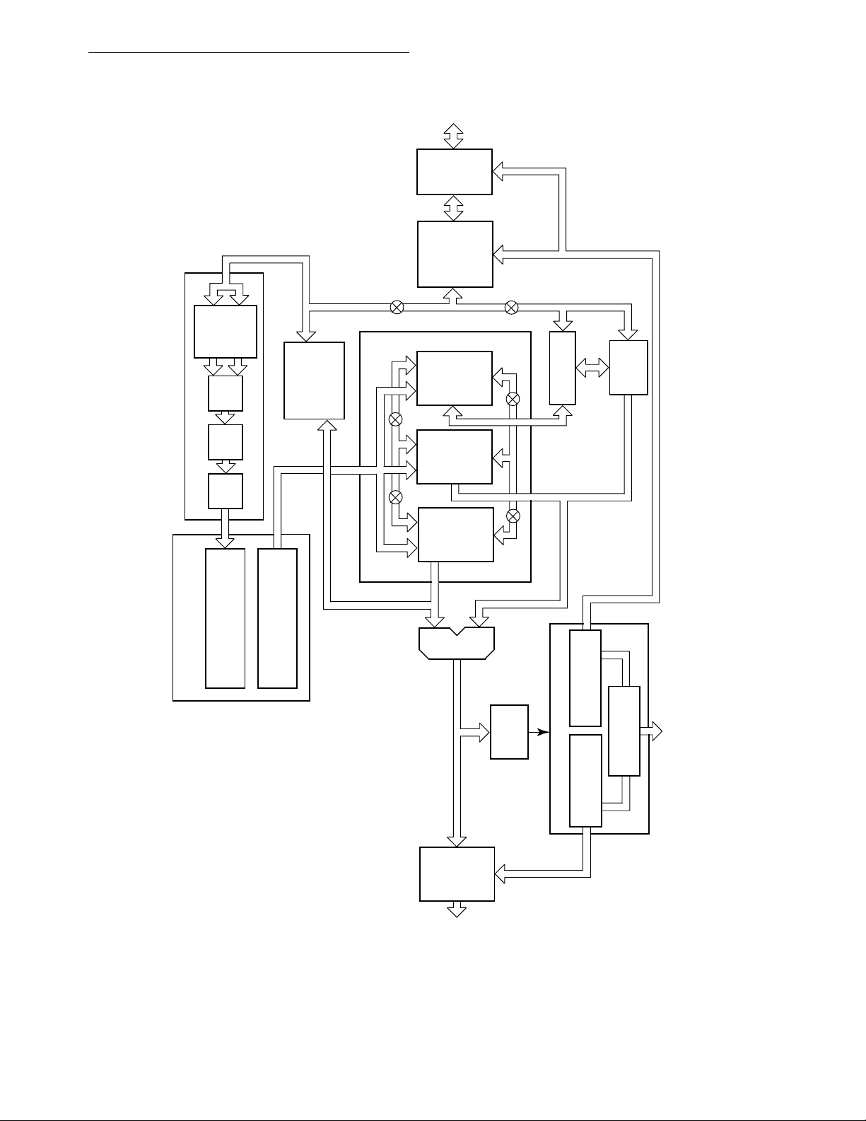
Introduction
BUS
DATA
DATA
PADS
INTERNAL
DATA
CACHE
HOLDING
REGISTER
B
STAGE
BUS
(CAHR)
CACHE
INSTRUCTION
SIZE
MULTIPLEXER
DATA
SECTION
DATA
MULTIPLEXER
MISALIGNMENT
CACHE
C
STAGE
INSTRUCTION PIPE
D
STAGE
STORE
CONTROL
CONTROL
MICROSEQUENCER AND
LOGIC
CONTROL
EXECUTION UNIT
BUS
ADDRESS
INSTRUCTION
SECTION
ADDRESS
SECTION
COUNTER
PROGRAM
ADDRESS
BUS
ADDRESS
UNIT
ACCESS
CONTROL
BUS
DATA
ADDRESS
BUFFER
PREFETCH PENDING
MICROBUS
BUS CONTROLLER
WRITE PENDING
CONTROLLER
BUFFER
SIGNALS
BUS CONTROL
1-2
PADS
ADDRESS
BUS
ADDRESS
Figure 1-1. Block Diagram
MC68030 USER’S MANUAL
MOTOROLA
Page 26

1.1 FEATURES
The features of the MC68030 microprocessor are:
• Object Code Compatible with the MC68020 and Earlier M68000 Microprocessors
• Complete 32-Bit Nonmultiplexed Address and Data Buses
• 16 32-Bit General-Purpose Data and Address Registers
• Two 32-Bit Supervisor Stack Pointers and 10 Special-Purpose Control Registers
• 256-Byte Instruction Cache and 256-Byte Data Cache Can Be Accessed Simultaneously
• Paged MMU that Translates Addresses in Parallel with Instruction Execution and Internal Cache Accesses
• Two Transparent Segments Allow Untranslated Access to Physical Memory To Be D
fined for Systems That Transfer Large Blocks of Data between Predefined Physical Addresses — e.g., Graphics Applications
• Pipelined Architecture with Increased Parallelism Allows Accesses to Internal Caches
To Occur in Parallel with Bus Transfers and Instruction Execution To Be Overlapped
Introduction
• Enhanced Bus Controller Supports Asynchronous Bus Cycles (three clocks minimum),
Synchronous Bus Cycles (two clocks minimum), and Burst Data Transfers (one clock
minimum) all to the Physical Address Space
• Dynamic Bus Sizing Supports 8-, 16-, 32-Bit Memories and Peripherals
• Support for Coprocessors with the M68000 Coprocessor Interface — e.g., Full IEEE
Floating-Point Support Provided by the MC68881/MC68882 Floating-Point Coprocessors
• 4-Gbyte Logical and Physical Addressing Range
• Implemented in Motorola's HCMOS Technology That Allows CMOS and HMOS (HighDensity NMOS) Gates to be Combined for Maximum Speed, Low Power, and Optimum
Die Size
• Processor Speeds Beyond 20 MHz
Both improved performance and increased functionality result from the on-chip
implementation of the MMU and the data and instruction caches. The enhanced bus
controller and the internal parallelism also provide increased system performance. Finally,
the improved bus interface, the reduction in physical size, and the lower power consumption
combine to reduce system costs and satisfy cost/performance goals of the system designer.
MOTOROLA
MC68030 USER’S MANUAL
1-3
Page 27

Introduction
1.2 MC68030 EXTENSIONS TO THE M68000 FAMILY
In addition to the on-chip instruction cache present in the MC68020, the MC68030 has an
internal data cache. Data that is accessed during read cycles may be stored in the on-chip
cache, where it is available for subsequent accesses. The data cache reduces the number
of external bus cycles when the data operand required by an instruction is already in the
data cache.
Performance is enhanced further because the on-chip caches can be internally accessed in
a single clock cycle. In addition, the bus controller provides a two-clock cycle synchronous
mode and burst mode accesses that can transfer data in as little as one clock per long word.
The MC68030 enhanced microprocessor contains an on-chip MMU that allows address
translation to operate in parallel with the CPU core, the internal caches, and the bus
controller.
Additional signals support emulation and system analysis. External debug equipment can
disable the on-chip caches and the MMU to freeze the MC68030 internal state during
breakpoint processing. In addition, the MC68030 indicates:
1. The start of a refill of the instruction pipe
2. Instruction boundaries
3. Pending trace or interrupt processing
4. Exception processing
5. Halt conditions
This status and control information allows external debugging equipment to trace the
MC68030 activity and interact nonintrusively with the MC68030 to effectively reduce system
debug effort.
1.3 PROGRAMMING MODEL
The programming model of the MC68030 consists of two groups of registers: the user model
and the supervisor model. This corresponds to the user and supervisor privilege levels. User
programs executing at the user privilege level use the registers of the user model. System
software executing at the supervisor level uses the control registers of the supervisor level
to perform supervisor functions.
1-4
MC68030 USER’S MANUAL
MOTOROLA
Page 28

Introduction
Figure 1-2 shows the user programming model, consisting of 16 32-bit general-purpose registers and two control registers:
• General-Purpose 32-Bit Registers (D0–D7, A0–A7)
• 32-Bit Program Counter (PC)
• 8-Bit Condition Code Register (CCR)
The supervisor programming model consists of the registers available to the user plus 14
control registers:
• Two 32-Bit Supervisor Stack Pointers (ISP and MSP)
• 16-Bit Status Register (SR)
• 32-Bit Vector Base Register (VBR)
• 32-Bit Alternate Function Code Registers (SFC and DFC)
• 32-Bit Cache Control Register (CACR)
• 32-Bit Cache Address Register (CAAR)
• 64-Bit CPU Root Pointer (CRP)
• 64-Bit Supervisor Root Pointer (SRP)
• 32-Bit Translation Control Register (TC)
• 32-Bit Transparent Translation Registers (TT0 and TT1)
• 16-Bit MMU Status Register (MMUSR)
The user programming model remains unchanged from previous M68000 Family
microprocessors. The supervisor programming model supplements the user programming
model and is used exclusively by the MC68030 system programmers who utilize the
supervisor privilege level to implement sensitive operating system functions, I/O control, and
memory management subsystems. The supervisor programming model contains all the
controls to access and enable the special features of the MC68030. This segregation was
carefully planned so that all application software is written to run at the nonprivileged user
level and migrates to the MC68030 from any M68000 platform without modification. Since
system software is usually modified by system programmers when ported to a new design,
the control features are properly placed in the supervisor programming model. For example,
the transparent translation feature of the MC68030 is new to the family supervisor
programming model for the MC68030 and the two translation registers are new additions to
the family supervisor programming model for the MC68030. Only supervisor code uses this
feature, and user application programs remain unaffected.
MOTOROLA
MC68030 USER’S MANUAL
1-5
Page 29
Introduction
Registers D0–D7 are used as data registers for bit and bit field (1 to 32 bits), byte (8 bit),
word (16 bit), long-word (32 bit), and quad-word (64 bit) operations. Registers A0–A6 and
the user, interrupt, and master stack pointers are address registers that may be used as
software stack pointers or base address registers. Register A7 (shown as A7' and A7'' in
Figure 1-3) is a register designation that applies to the user stack pointer in the user privilege
level and to either the interrupt or master stack pointer in the supervisor privilege level. In
the supervisor privilege level, the active stack pointer (interrupt or master) is called the
supervisor stack pointer (SSP). In addition, the address registers may be used for word and
long-word operations. All of the 16 general-purpose registers (D0–D7, A0–A7) may be used
as index registers.
31 16 15
31 16 15 0
31
31
16 15
15
87
7
0
D0
D1
D2
D3
D4
D5
D6
D7
A0
A1
A2
A3
A4
A5
A6
0
A7 (USP)
0
PC
0
CCR
DATA
REGISTERS
ADDRESS
REGISTERS
USER STACK
POINTER
PROGRAM
COUNTER
CONDITION
CODE
REGISTER
1-6
Figure 1-2. User Programming Model
MC68030 USER’S MANUAL
MOTOROLA
Page 30
Introduction
The program counter (PC) contains the address of the next instruction to be executed by the
MC68030. During instruction execution and exception processing, the processor
automatically increments the contents of the PC or places a new value in the PC, as
appropriate.
31
31
31
31
31
31
31
31
16 15
16 15
15
15
0
0
87 0
(CCR) SR
0
0
0
0
0
0
0
A7' (ISP)
A7" (MSP)
VBR
SFC
DFC
CACR
CAAR
AC0
AC1
ACUSR
INTERRUPT
STACK POINTER
MASTER STACK
POINTER
STATUS REGISTER
VECTOR BASE
REGISTER
ALTERNATE FUNCTION
CODE REGISTERS
CACHE CONTROL
REGISTER
CACHE ADDRESS
REGISTER
ACCESS
CONTROL
REGISTER 0
ACCESS
CONTROL
REGISTER 1
ACU STATUS
REGISTER
Figure 1-3. Supervisor Programming Model Supplement
The status register, SR, (see Figure 1-4) stores the processor status. It contains the
condition codes that reflect the results of a previous operation and can be used for
conditional instruction execution in a program. The condition codes are extend (X), negative
(N), zero (Z), overflow (V), and carry (C). The user byte containing the condition codes is the
only portion of the status register information available in the user privilege level, and it is
referenced as the CCR in user programs. In the supervisor privilege level, software can
access the full status register, including the interrupt priority mask (three bits) as well as
additional control bits. These bits indicate whether the processor is in:
1. One of two trace modes (T1, T0)
2. Supervisor or user privilege level (S)
3. Master or interrupt mode (M)
The vector base register (VBR) contains the base address of the exception vector table in
memory. The displacement of an exception vector is added to the value in this register to
access the vector table.
MOTOROLA
MC68030 USER’S MANUAL
1-7
Page 31

Introduction
Alternate function code registers, SFC and DFC, contain 3-bit function codes. Function
codes can be considered extensions of the 32-bit linear address that optionally provide as
many as eight 4-Gbyte address spaces. Function codes are automatically generated by the
processor to select address spaces for data and program at the user and supervisor
privilege levels and a CPU address space for processor functions (e.g., coprocessor
communications). Registers SFC and DFC are used by certain instructions to explicitly
specify the function codes for operations.
USER BYTE
(CONDITION CODE REGISTER)
CARRY
OVERFLOW
ZERO
NEGATIVE
EXTEND
15 14 13 12 11 10 9 8 7 56 43210
T1 T0 S M 0 I2 I1 I0 X N Z V C000
TRACE
ENABLE
SUPERVISOR/USER
STATE
MASTER/INTERRUPT
STATE
SYSTEM BYTE
INTERRUPT
PRIORITY MASK
Figure 1-4. Status Register
The cache control register (CACR) controls the on-chip instruction and data caches of the
MC68030. The cache address register (CAAR) stores an address for cache control
functions.
The CPU root pointer (CRP) contains a pointer to the root of the translation tree for the
currently executing task of the MC68030. This tree contains the mapping information for the
task's address space. When the MC68030 is configured to provide a separate address
space for supervisor routines, the supervisor root pointer (SRP) contains a pointer to the root
of the translation tree describing the supervisor's address space.
The translation control register (TC) consists of several fields that control address
translation. These fields enable and disable address translation, enable and disable the use
of SRP for the supervisor address space, and select or ignore the function codes in
translating addresses. Other fields define the size of memory pages, the number of address
bits used in translation, and the translation table structure.
The transparent translation registers, TT0 and TT1, can each specify separate blocks of
memory as directly accessible without address translation. Logical addresses in these areas
become the physical addresses for memory access. Function codes and the eight most
significant bits of the address can be used to define the area of memory and type of access;
either read, write, or both types of memory access can be directly mapped. The transparent
translation feature allows rapid movement of large blocks of data in memory or I/O space
without disturbing the context of the on-chip address translation cache or incurring delays
associated with translation table lookups. This feature is useful to graphics, controller, and
real-time applications.
1-8
MC68030 USER’S MANUAL
MOTOROLA
Page 32

Introduction
The MMU status register (MMUSR) contains memory management status information
resulting from a search of the address translation cache or the translation tree for a particular
logical address.
1.4 DATA TYPES AND ADDRESSING MODES
Seven basic data types are supported:
1. Bits
2. Bit Fields (Fields of consecutive bits, 1–32 bits long)
3. BCD Digits (Packed: 2 digits/byte, Unpacked: 1 digit/byte)
4. Byte Integers (8 bits)
5. Word Integers (16 bits)
6. Long-Word Integers (32 bits)
7. Quad-Word Integers (64 bits)
In addition, the instruction set supports operations on other data types such as memory
addresses. The coprocessor mechanism allows direct support of floating-point operations
with the MC68881 and MC68882 floating-point coprocessors as well as specialized userdefined data types and functions.
The 18 addressing modes, shown in Table 1-1, include nine basic types:
1. Register Direct
2. Register Indirect
3. Register Indirect with Index
4. Memory Indirect
5. Program Counter Indirect with Displacement
6. Program Counter Indirect with Index
7. Program Counter Memory Indirect
8. Absolute
9. Immediate
The register indirect addressing modes can also postincrement, predecrement, offset, and
index addresses. The program counter relative mode also has index and offset capabilities.
As in the MC68020, both modes are extended to provide indirect reference through memory.
In addition to these addressing modes, many instructions implicitly specify the use of the
condition code register, stack pointer, and/or program counter.
1.5 INSTRUCTION SET OVERVIEW
The instructions in the MC68030 instruction set are listed in Table 1-2. The instruction set
has been tailored to support structured high-level languages and sophisticated operating
systems. Many instructions operate on bytes, words, or long words, and most instructions
can use any of the 18 addressing modes.
MOTOROLA
MC68030 USER’S MANUAL
1-9
Page 33

Introduction
Table 1-1. Addressing Modes
Addressing Modes Syntax
Register Direct
Data Register Direct
Address Register Direct
Register Indirect
Address Register Indirect
Address Register Indirect with Postincrement
Address Register Indirect with Predecrement
Address Register Indirect with Displacement
Register Indirect with Index
Address Register Indirect with Index (8-BitDisplacement)
Address Register Indirect with Index (Base Displacement)
Memory Indirect
Memory Indirect Postindexed
Memory Indirect Preindexed
Program Counter Indirect with Displacement
Program Cou nter Indirect with IndexPC Indirect with Index (8-Bit
Displacement)
PC Indirect with Index (Base Displacement)
Program Counter Memory Indirect
PC Memory Indirect Postindexed
PC Memory Indirect Preindexed
Absolute
Absolute Short
Absolute Long
Immediate #(data)
Dn
An
(An)
(An)
–(An)
(d
,An)
16
(d
,An,Xn)
8
(bd,An,Xn)
([bd,An],Xn,od)
([bd,An,Xn],od)
(d
,PC)
16
(d
,PC,Xn)
8
(bd,PC,Xn)
([bd,PC],Xn,od)
([bd,PC,Xn],od)
(xxx).W
(xxx).L
NOTES:
Dn = Data Register, D0–D7
An = Address Register, A0–A7
d
8,
16 = A twos-complement or sign-extended displacement; added as part of the effective address
calculation; size is 8 (d
) or 16 (d
8
) bits; when omitted, assemblers use a value of zero.
16
Xn = Address or data register used as an index register; form is Xn.SIZE*SCALE, where SIZE is .W
or .L indicates index register size) and SCALE is 1, 2, 4, or 8 (index register is multiplied by
SCALE); use of SIZE and/or SCALE is optional.
bd = A twos-complement base displacement;when present, size can be 16 or 32 bits.
od = Outer displacement, added as part of effective address calculation after any memory
indirection; use is optional with asize of 16 or 32 bits.
PC = Program Counter
(data) = Immediate value of 8, 16, or 32 bits
( ) = Effective Address
[ ] = Use as indirect access to long-word address.
1-10
MC68030 USER’S MANUAL
MOTOROLA
Page 34

Introduction
1.6 VIRTUAL MEMORY AND VIRTUAL MACHINE CONCEPTS
The full addressing range of the MC68030 is 4 Gbytes (4,294,967,296 bytes) in each of eight
address spaces. Even though most systems implement a smaller physical memory, the
system can be made to appear to have a full 4 Gbytes of memory available to each user
program by using virtual memory techniques.
In a virtual memory system, a user program can be written as if it has a large amount of
memory available, when the physical memory actually present is much smaller. Similarly, a
system can be designed to allow user programs to access devices that are not physically
present in the system, such as tape drives, disk drives, printers, terminals, and so forth. With
proper software emulation, a physical system can appear to be any other M68000 computer
system to a user program, and the program can be given full access to all of the resources
of that emulated system. Such an emulated system is called a virtual machine.
1.6.1 Virtual Memory
A system that supports virtual memory has a limited amount of high-speed physical memory
that can be accessed directly by the processor and maintains an image of a much larger
virtual memory on a secondary storage device such as a large-capacity disk drive. When
the processor attempts to access a location in the virtual memory map that is not resident in
physical memory, a page fault occurs. The access to that location is temporarily suspended
while the necessary data is fetched from secondary storage and placed in physical memory.
The suspended access is then either restarted or continued.
The MC68030 uses instruction continuation to support virtual memory. When a bus cycle is
terminated with a bus error, the microprocessor suspends the current instruction and
executes the virtual memory bus error handler. When the bus error handler has completed
execution, it returns control to the program that was executing when the error was detected,
reruns the faulted bus cycle (when required), and continues the suspended instruction.
MOTOROLA
MC68030 USER’S MANUAL
1-11
Page 35

Introduction
Table 1-2. Instruction Set
Mnemonic Description Mnemonic Description
ABCD Add Decimal with Extend MOVE USP Move User Stack Pointer
ADD Add MOVEC Move Control Register
ADDA Add Address MOVEM Move Multiple Registers
ADDI Add Immediate MOVEP Move Periphral
ADDQ Add Quick MOVEQ Move Quick
ADDX Add with Extend MOVES Move Alternate Address Space
AND Logical AND MULS Signed Multiply
ANDI Logical AND Immediate MULU Unsigned Multiply
ASL, ASR Arithmatic Shift Left and Right NBCD Negate Decimal with Extend
Bcc Branch Conditionally NEG Negate
BCHG Test Bit and Change NEGX Negate with Extend
BCLR Test Bit and Clear NOP No Operation
BFCHG Test Bit Feild and Change NOT Logical Compliment
BFCLR Test Bit Feild and Clear OR Logical Inclusive OR
BFEXTS Signed Bit Feild Extract ORI Logical Inclusive OR Immediate
BFEXTU Unsigned Bit Feild Extract ORI CCR Logical Inclusive OR Immediate to
BFFO Bit Feild Find First One Condition Codes
BFINS Bit Feild Insert ORI SR Logical Inclusive OR Immediate to
BFSET Test Bit Feild and Set Status Register
BFTST Test Bit Feild PACK Pack BCD
BKPT Breakpoint PEA Push Effective Address
BRA Branch PFLUSH Flush Entry(ies) in the ATC
BSET Test Bit and Set PFLUSHA Flush All Entries in the ATC
BSR Branch to Subroutine PLOADR, Load Entry into the ATC
BTST Test Bit PLOADW
CAS Compare and Swap Operands PMOVE Move to-from MMU Registers
CAS 2 Compare and Swap Dual Operands PMOVEFD Move to-from MMU Registers with
CHK Check Register Against Bound Flush Disable
CHK2 Check Register Against Upper and PTESTR Test a Logical Address
Lower Bounds PTESTW
CLR Clear RESET Reset External Devices
CMP Compare ROL, ROR Rotate Left and Right
CMPA Compare Address ROXL, ROXR Rotate With Extend Left and Right
CMPI Compare Immediate RTD Return and Deallocate
CMPM Compare Memory to Memory RTE Return from Exception
CMP2 Compare Registre Against Upper and RTR Return and Restore Codes
Lower Bounds RTS Return from Subroutine
DBcc Test Condition, Decrement and Branch SBCD Subtract Decimal With Extend
DIVS, DIVSL Signed Divide Scc Set Conditionally
DIVU, DIVUL Unsigned Divide STOP Stop
EOR Logical Exclusive OR SUB Subtract
EORI Logical Exclusive OR Immediate SUBA Subtract Immediate
EXG Exchange Registers SUBI Subtract Quick
EXT, EXTB Sign Extend SUBQ Subtract with Extend
ILLEGAL Take Illegal Instruction Trap SUBX Swap Register Words
JMP Jump SWAP Test Operand and Set
JSR Jump to Subroutine TAS Trap
LEA Load Effective Address TRAP Trap Conditionally
LINK Link and Allocate TRAPcc Trap on Overflow
LSL, LSR Logical Shift Left and Right TRAPV Test on Overflow
MOVE Move TST Test Operand
MOVEA Move Address
MOVE CCR Move Condition Code Register
MOVE SR Move Status Register
UNLK
UNPK
Unlink
Unpack BCD
1-12
MC68030 USER’S MANUAL
MOTOROLA
Page 36

Introduction
Mnemonic Description Mnemonic Description
cpBcc
cpDBcc
cpGEN
Branch Conditionally
Test Coprocessor Condition,
Decrement and Branch
Coprocessor General Instruction
cpRESTORE
cpSAVE
cpScc
cpTRAPcc
Restore Internal State of Coprocessor
Save Internal State of Coprocessor
Set Conditionally
Trap Conditionally
1.6.2 Virtual Machine
A typical use for a virtual machine system is the development of software, such as an
operating system, for a new machine also under development and not yet available for
programming use. In a virtual machine system, a governing operating system emulates the
hardware of the new machine and allows the new software to be executed and debugged
as though it were running on the new hardware. Since the new software is controlled by the
governing operating system, it is executed at a lower privilege level than the governing
operating system. Thus, any attempts by the new software to use virtual resources that are
not physically present (and should be emulated) are trapped to the governing operating
system and performed by its software.
In the MC68030 implementation of a virtual machine, the virtual application runs at the user
privilege level. The governing operating system executes at the supervisor privilege level
and any attempt by the new operating system to access supervisor resources or execute
privileged instructions causes a trap to the governing operating system.
Instruction continuation is used to support virtual I/O devices in memory-mapped input/
output systems. Control and data registers for the virtual device are simulated in the memory
map. An access to a virtual register causes a fault and the function of the register is
emulated by software.
MOTOROLA
MC68030 USER’S MANUAL
1-13
Page 37

Introduction
1.7 THE MEMORY MANAGEMENT UNIT
The MMU supports virtual memory systems by translating logical addresses to physical addresses using translation tables stored in memory. The MMU stores address mappings in
an address translation cache (ATC) that contains the most recently used translations. When
the ATC contains the address for a bus cycle requested by the CPU, a translation table
search is not performed. Features of the MMU include:
• Multiple Level Translation Tables with Short- and Long-Format Descriptors for Efficient
Table Space Usage
• Table Searches Automatically Performed in Microcode
• 22-Entry Fully Associative ATC
• Address Translations and Internal Instruction and Data Cache Accesses Performed in
Parallel
• Eight Page Sizes Available Ranging from 256 to 32K Bytes
• Two Optional Transparent Blocks
• User and Supervisor Root Pointer Registers
• Write Protection and Supervisor Protection Attributes
• Translations Enabled/Disabled by Software
• Translations Can Be Disabled with External MMUDIS
Signal
• Used and Modified Bits Automatically Maintained in Tables and ATC
• Cache Inhibit Output (CIOUT
) Signal Can Be Asserted on a Page-by-Page Basis
• 32-Bit Internal Logical Address with Capability To Ignore as many as 15 Upper Address
Bits
• 3-Bit Function Code Supports Separate Address Spaces
• 32-Bit Physical Address
The memory management function performed by the MMU is called demand paged memory
management. Since a task specifies the areas of memory it requires as it executes, memory
allocation is supported on a demand basis. If a requested access to memory is not currently
mapped by the system, then the access causes a demand for the operating system to load
or allocate the required memory image. The technique used by the MC68030 is paged
memory management because physical memory is managed in blocks of a specified
number of bytes, called page frames. The logical address space is divided into fixed-size
pages that contain the same number of bytes as the page frames. Memory management
assigns a physical base address to a logical page. The system software then transfers data
between secondary storage and memory one or more pages at a time.
1-14
MC68030 USER’S MANUAL
MOTOROLA
Page 38

Introduction
1.8 PIPELINED ARCHITECTURE
The MC68030 uses a three-stage pipelined internal architecture to provide for optimum
instruction throughput. The pipeline allows as many as three words of a single instruction or
three consecutive instructions to be decoded concurrently.
1.9 THE CACHE MEMORIES
Due to locality of reference, instructions and data that are used in a program have a high
probability of being reused within a short time. Additionally, instructions and data operands
that reside in proximity to the instructions and data currently in use also have a high
probability of being utilized within a short period. To exploit these locality characteristics, the
MC68030 contains two on-chip logical caches, a data cache, and an instruction cache.
Each of the caches stores 256 bytes of information, organized as 16 entries, each containing
a block of four long words (16 bytes). The processor fills the cache entries either one long
word at a time or, during burst mode accesses, four long words consecutively. The burst
mode of operation not only fills the cache efficiently but also captures adjacent instruction or
data items that are likely to be required in the near future due to locality characteristics of
the executing task.
The caches improve the overall performance of the system by reducing the number of bus
cycles required by the processor to fetch information from memory and by increasing the
bus bandwidth available for other bus masters in the system. Addition of the data cache in
the MC68030 extends the benefits of cache techniques to all memory accesses. During a
write cycle, the data cache circuitry writes data to a cached data item as well as to the item
in memory, maintaining consistency between data in the cache and that in memory.
However, writing data that is not in the cache may or may not cause the data item to be
stored in the cache, depending on the write allocation policy selected in the cache control
register (CACR).
MOTOROLA
MC68030 USER’S MANUAL
1-15
Page 39

SECTION 2
DATA ORGANIZATION AND ADDRESSING
CAPABILITIES
Most external references to memory by a microprocessor are either program references or
data references; they either access instruction words or operands (data items) for an
instruction. Program references are references to the program space, the section of memory
that contains the program instructions and any immediate data operands that reside in the
instruction stream. Refer to M68000PM/AD,
descriptions of the instructions in the program space. Data references refer to the data
space, the section of memory that contains the program data. Data items in the instruction
stream can be accessed with the program counter relative addressing modes, and these
accesses are classified as program references. A third type of external reference used for
coprocessor communications, interrupt acknowledge cycles, and breakpoint acknowledge
cycles is classified as a CPU space reference. The MC68030 automatically sets the function
codes to access the program space, the data space, or the CPU space for special functions
as required. The function codes can be used by the memory management unit to organize
separate program (read only) and data (read-write) memory areas.
M68000 Programmer's Reference Manual
, for
This section describes the data organization and addressing capabilities of the MC68030. It
lists the types of operands used by instructions and describes the registers and their use as
operands. Next, the section describes the organization of data in memory and the
addressing modes available to access data in memory. Last, the section describes the
system stack and user program stacks and queues.
2.1 INSTRUCTION OPERANDS
The MC68030 supports a general-purpose set of operands to serve the requirements of a
large range of applications. Operands of MC68030 instructions may reside in registers, in
memory, or within the instructions themselves. An instruction operand might also reside in
a coprocessor. An operand may be a single bit, a bit field of from 1 to 32 bits in length, a byte
(8 bits), a word (16 bits), a long word (32 bits), or a quad word (64 bits). The operand size
for each instruction is either explicitly encoded in the instruction or implicitly defined by the
instruction operation. Coprocessors are designed to support special computation models
that require very specific but widely varying data operand types and sizes. Hence,
coprocessor instructions can specify operands of any size.
MOTOROLA
MC68030 USER’S MANUAL
2-1
Page 40

Data Organization and Addressing Capabilities
2.2 ORGANIZATION OF DATA IN REGISTERS
The eight data registers can store data operands of 1, 8, 16, 32, and 64 bits, addresses of
16 or 32 bits, or bit fields of 1 to 32 bits. The seven address registers and the three stack
pointers are used for address operands of 16 or 32 bits. The control registers (SR, VBR,
SFC, DFC, CACR, CAAR, CRP, SRP, TC, TT0, TT1, and MMUSR) vary in size according
to function. Coprocessors may define unique operand sizes and support them with on-chip
registers accordingly.
2.2.1 Data Registers
Each data register is 32 bits wide. Byte operands occupy the low-order 8 bits, word
operands the low-order 16 bits, and long-word operands the entire 32 bits. When a data
register is used as either a source or destination operand, only the appropriate low-order
byte or word (in byte or word operations, respectively) is used or changed; the remaining
high-order portion is neither used nor changed. The least significant bit of a long-word
integer is addressed as bit zero, and the most significant bit is addressed as bit 31. For bit
fields, the most significant bit is addressed as bit zero, and the least significant bit is
addressed as the width of the field minus one. If the width of the field plus the offset is greater
than 32, the bit field wraps around within the register. The following illustration shows the
organization of various types of data in the data registers.
Quad-word data consists of two long words; for example, the product of 32-bit multiply or
the quotient of 32-bit divide operations (signed and unsigned). Quad words may be
organized in any two data registers without restrictions on order or pairing. There are no
explicit instructions for the managment of this data type, although the MOVEM instruction
can be used to move a quad word into or out of the registers.
Binary-coded decimal (BCD) data represents decimal numbers in binary form. Although
many BCD codes have been devised, the BCD instructions of the M68000 Family support
formats which the four least significant bits consist of a binary number having the numeric
value of the corresponding decimal number. Two BCD formats are used. In the unpacked
BCD format, a byte contains one digit; the four least significant bits contain the binary value
and the four most significant bits are undefined. Each byte of the packed BCD format
contains two digits; the least significant four bits contain the least significant digit.
2-2
MC68030 USER’S MANUAL
MOTOROLA
Page 41

Data Organization and Addressing Capabilities
Bit ≤ (0 Modulo (Offset)<31, Offset of 0 = MSB)
31 30 29 10
MSB
•••
Byte
31 24 23 16 15 8 7 0
High-Order Byte Middle-High Byte Middle-Low Byte Low-Order Byte
16-Bit Word
31 16 15 0
High-Order Word Low-Order Word
Long Word
31 0
Long Word
LSB
Quad Word
63 62 32
MSB Any Dx
31 0
Offset MSB
•••
LSB
Bit Field (0 ≤ Offset<32, 0<Width ≤ 32)
31 0
Long Word
Note: If width + offset < 32, bit filed wraps around within the register.
Unpacked BCD (a = MSB)
31 876543210
xxxxabcd
Packed BCD (a = MSB First Digit, e = MSB Second Digit)
31 876543210
abcdefgh
MOTOROLA
Data Organization in Data Registers
MC68030 USER’S MANUAL
2-3
Page 42

Data Organization and Addressing Capabilities
2.2.2 Address Registers
Each address register and stack pointer is 32 bits wide and holds a 32-bit address. Address
registers cannot be used for byte-sized operands. Therefore, when an address register is
used as a source operand, either the low-order word or the entire long-word operand is
used, depending upon the operation size. When an address register is used as the
destination operand, the entire register is affected, regardless of the operation size. If the
source operand is a word size, it is first sign-extended to 32 bits and then used in the
operation to an address register destination. Address registers are used primarily for
addresses and to support address computation. The instruction set includes instructions
that add to, subtract from, compare, and move the contents of address registers. The
following example shows the organization of addresses in address registers.
31 16 15 0
Sign-Extended 16-Bit Address Operand
31 0
Full 32-Bit Address Operand
Address Organization in Address Registers
2.2.3 Control Registers
The control registers described in this section contain control information for supervisor
functions and vary in size. With the exception of the user portion of the status register (CCR),
they are accessed only by instructions at the supervisor privilege level.
The status register (SR), shown in Figure 1–4, is 16 bits wide. Only 12 bits of the status
register are defined; all undefined values are reserved by Motorola for future definition. The
undefined bits are read as zeros and should be written as zeros for future compatibility. The
lower byte of the status register is the CCR. Operations to the CCR can be performed at the
supervisor or user privilege level. All operations to the status register and CCR are wordsized operations, but for all CCR operations, the upper byte is read as all zeros and is
ignored when written, regardless of privilege level.
2-4
MC68030 USER’S MANUAL
MOTOROLA
Page 43

Data Organization and Addressing Capabilities
The supervisor programming model (see Figure 1–3) shows the control registers. The cache
control register (CACR) provides control and status information for the on-chip instruction
and data caches. The cache address register (CAAR) contains the address for cache control
functions. The vector base register (VBR) provides the base address of the exception vector
table. All operations involving the CACR, CAAR, and VBR are long-word operations,
whether these registers are used as the source or the destination operand.
The alternate function code registers (SFC and DFC)
are 32-bit registers with only bits 2:0 implemented that contain the address space values
(FC0-FC2) for the read or write operands of MOVES, PLOAD, PFLUSH, and PTEST
instructions. The MOVEC instruction is used to transfer values to and from the alternate
function code registers. These are long-word transfers; the upper 29 bits are read as zeros
and are ignored when written.
The remaining control registers in the supervisor programming model are used by the
memory management unit (MMU). The CPU root pointer (CRP) and supervisor root pointer
(SRP) contain pointers to the user and supervisor address translation trees. Transfers of
data to and from these 64-bit registers are quad-word transfers. The translation control
register (TC) contains control information for the MMU. The MC68030 always uses longword transfers to access this 32-bit register. The transparent translation registers (TT0 and
TT1) also contain 32 bits each; they identify memory areas for direct addressing without
address translation. Data transfers to and from these registers are long-word transfers. The
MMU status register (MMUSR) stores the status of the MMU after execution of a PTEST
instruction. It is a 16-bit register, and transfers to and from the MMUSR are word transfers.
Refer to Section 9 Memory Management Unit for more detail.
2.3 ORGANIZATION OF DATA IN MEMORY
Memory is organized on a byte-addressable basis where lower addresses correspond to
higher order bytes. The address, N, of a long-word data item corresponds to the address of
the most significant byte of the highest order word. The lower order word is located at
address N + 2, leaving the least significant byte at address N + 3 (refer to Figure 2–1). Notice
that the MC68030 does not require data to be aligned on word boundaries (refer to Figure
2–2), but the most efficient data transfers occur when data is aligned on the same byte
boundary as its operand size. However, instruction words must be aligned on word
boundaries.
MOTOROLA
MC68030 USER’S MANUAL
2-5
Page 44

Data Organization and Addressing Capabilities
The data types supported in memory by the MC68030 are bit and bit field data; integer data
of 8, 16, or 32 bits; 32-bit addresses; and BCD data (packed and unpacked). These data
types are organized in memory as shown in Figure 2–2. Note that all of these data types can
be accessed at any byte address.
Coprocessors can implement any data types and lengths up to 255 bytes. For example, the
MC68881/MC68882 floating-point coprocessors support memory accesses for quad-wordsized items (double-precision floating-point values).
Figure 2A bit operand is specified by a base address that selects one byte in memory (the
base byte) and a bit number that selects the one bit in this byte. The most significant bit of
the byte is bit 7.
31 23 15 7 0
LONG WORD $00000000
WORD $00000000
BYTE $00000000
WORD $00000004
BYTE $00000004
WORD $FFFFFFFC
BYTE $FFFFFFFC
WORD $00000002
BYTE $00000001 BYTE $00000002 BYTE $00000003
LONG WORD $00000004
WORD $00000006
BYTE $00000005 BYTE $00000006 BYTE $00000007
LONG WORD $FFFFFFFC
WORD $FFFFFFFE
BYTE $FFFFFFFD BYTE $FFFFFFFE BYTE $FFFFFFFF
Figure 2-1. Memory Operand Address
2-6
MC68030 USER’S MANUAL
MOTOROLA
Page 45

BYTE n - 1
Data Organization and Addressing Capabilities
BIT DATA
07707070
BYTE n - 1 BYTE n + 1
BASE ADDRESS BIT NUMBER
BYTE n - 1
OFFSET
BYTE n - 1 BYTE n + 2
0
77
7 6 5 4 3 2 1 0 BYTE n + 2
BIT FIELD DATA BASE BIT
07707070
BYTE n 0 1 2 3 ...........w - 1
WIDTHOFFSET
...3-2-1 0 1 2...
BASE ADDRESS
07707070
ADDRESS
WORD INTEGER DATA
0
07 07 07 0
7
WORD INTEGER BYTE n + 2 BYTE n + 3
BYTE INTEGER DATA
BYTE n + 1MSB BYTE n LSB
0
77
BYTE n - 1
ADDRESS
ADDRESS
0
77
BYTE n - 1
XX = USER DEFINED VALUE
ADDRESS
0
7
70
70
LONG-WORD INTEGER BYTE n + 4
QUAD-WORD DATA
BYTE n - 1 BYTE n + 2BYTE n + 1MSD LSD
BYTE n - 1 BYTE n + 2
70
QUAD WORD
PACKED BINARY-CODED DATA
07707070
ADDRESS
077 07070
ADDRESS
43
UNPACKED BINARY-CODED DATA
43
XX MSD
07 07 0
07 07 0
BYTE n + 8
43
XX LSD
MOTOROLA
Figure 2-2. Memory Data Organization
MC68030 USER’S MANUAL
2-7
Page 46

Data Organization and Addressing Capabilities
A bit field operand is specified by:
1. A base address that selects one byte in memory,
2. A bit field offset that indicates the leftmost (base) bit of the bit field in relation to the
most significant bit of the base byte, and
3. A bit field width that determines how many bits to the right of the base bit are in the bit
field.
The most significant bit of the base byte is bit field offset 0, the least significant bit of the
base byte is bit field offset 7, and the least significant bit of the previous byte in memory is
bit offset –1. Bit field offsets may have values in the range of –2
31
to 2
31
–1, and bit field
widths may range between 1 and 32 bits.
2.4 ADDRESSING MODES
The addressing mode of an instruction can specify the value of an operand (with an
immediate operand), a register that contains the operand (with the register direct addressing
mode), or how the effective address of an operand in memory is derived. An assembler
syntax has been defined for each addressing mode.
Figure 2–3 shows the general format of the single effective address instruction operation
word. The effective address field specifies the addressing mode for an operand that can use
one of the numerous defined modes. The (eaL designation is composed of two 3-bit fields:
the mode field and the register field. The value in the mode field selects one or a set of
addressing modes. The register field specifies a register for the mode or a submode for
modes that do not use registers.
15
X X X X X X X X X X
14 13 12 11 10 9 8 7 6 5 0
EFFECTIVE ADDRESS
MODE REGISTER
Figure 2-3. Single Effective Address
Many instructions imply the addressing mode for one of the operands. The formats of these
instructions include appropriate fields for operands that use only one addressing mode.
2-8
MC68030 USER’S MANUAL
MOTOROLA
Page 47

Data Organization and Addressing Capabilities
The effective address field may require additional information to fully specify the operand
address. This additional information, called the effective address extension, is contained in
an additional word or words and is considered part of the instruction. Refer to 2.5 Effective
Address Encoding Summary for a description of the extension word formats.
The notational conventions used in the addressing mode descriptions in this section are:
EA — Effective address
An — Address register n
Example: A3 is address register 3
Dn — Data register n
Example: D5 is data register 5
Xn.SIZE*SCALE — Denotes index register n (data or address), the index size
(W for word, L for long word), and a scale factor (1, 2, 4,
or 8 for no, word, long-word, or quad-word scaling, respectively).
PC — The program counter
d
n
— Displacement value, n bits wide
bd — Base displacement
od — Outer displacement
L — Long-word size
W — Word size
( ) — Identify an indirect address in a register
[ ] — Identify an indirect address in memory
When the addressing mode uses a register, the register field of the operation word specifies
the register to be used. Other fields within the instruction specify whether the register
selected is an address or data register and how the register is to be used.
2.4.1 Data Register Direct Mode
In the data register direct mode, the operand is in the data register specified by the effective
address register field.
GENERATION:
ASSEMBLER SYNTAX:
MODE:
REGISTER:
DATA REGISTER:
NUMBER OF EXTENSION WORDS:
EA = Dn
Dn
000
n
Dn
0
31 0
OPERAND
OPERAND
MOTOROLA
MC68030 USER’S MANUAL
2-9
Page 48

Data Organization and Addressing Capabilities
2.4.2 Address Register Direct Mode
In the address register direct mode, the operand is in the address register specified by the
effective address register field.
GENERATION:
ASSEMBLER SYNTAX:
MODE:
REGISTER:
ADDRESS REGISTER:
NUMBER OF EXTENSION WORDS:
EA = An
An
001
n
An
0
31 0
OPERAND
2.4.3 Address Register Indirect Mode
In the address register indirect mode, the operand is in memory, and the address of the
operand is in the address register specified by the register field.
GENERATION:
ASSEMBLER SYNTAX:
MODE:
REGISTER:
ADDRESS REGISTER:
MEMORY ADDRESS:
NUMBER OF EXTENSION WORDS:
EA = (An)
(An)
010
n
An
0
31 0
MEMORY ADDRESS
31 0
OPERAND
2.4.4 Address Register Indirect with Postincrement Mode
In the address register indirect with postincrement mode, the operand is in memory, and the
address of the operand is in the address register specified by the register field. After the
operand address is used, it is incremented by one, two, or four depending on the size of the
operand: byte, word, or long word. Coprocessors may support incrementing for any size of
operand up to 255 bytes. If the address register is the stack pointer and the operand size is
byte, the address is incremented by two rather than one to keep the stack pointer aligned to
a word boundary.
GENERATION:
ASSEMBLER SYNTAX:
MODE:
REGISTER:
ADDRESS REGISTER:
OPERAND LENGTH ( 1, 2, OR 4):
MEMORY ADDRESS:
NUMBER OF EXTENSION WORDS:
EA = (An)
An = An + SIZE
(An) +
011
n
An
0
31 0
MEMORY ADDRESS
+
31 0
OPERAND
2-10
MC68030 USER’S MANUAL
MOTOROLA
Page 49

Data Organization and Addressing Capabilities
2.4.5 Address Register Indirect with Predecrement Mode
In the address register indirect with predecrement mode, the operand is in memory, and the
address of the operand is in the address register specified by the register field. Before the
operand address is used, it is decremented by one, two, or four depending on the operand
size: byte, word, or long word. Coprocessors may support decrementing for any operand
size up to 255 bytes. If the address register is the stack pointer and the operand size is byte,
the address is decremented by two rather than one to keep the stack pointer aligned to a
word boundary.
GENERATION:
ASSEMBLER SYNTAX:
MODE:
REGISTER:
ADDRESS REGISTER:
OPERAND LENGTH (1, 2, OR 4):
MEMORY ADDRESS:
NUMBER OF EXTENSION WORDS: 0
An = An – SIZE
EA = (An)
– (An)
100
n
An
31 0
MEMORY ADDRESS
31 0
OPERAND
MOTOROLA
MC68030 USER’S MANUAL
2-11
Page 50

Data Organization and Addressing Capabilities
2.4.6 Address Register Indirect with Displacement Mode
In the address register indirect with displacement mode, the operand is in memory. The
address of the operand is the sum of the address in the address register plus the signextended 16-bit displacement integer in the extension word. Displacements are always signextended to 32 bits prior to being used in effective address calculations.
GENERATION:
ASSEMBLER SYNTAX:
MODE:
REGISTER:
ADDRESS REGISTER:
DISPLACEMENT:
MEMORY ADDRESS:
NUMBER OF EXTENSION WORDS: 1
EA = (An) + d
(d ,An)
16
101
n
An
SIGN EXTENDED INTEGER
16
31 0
15
31 0
MEMORY ADDRESS
031
+
OPERAND
2.4.7 Address Register Indirect with Index (8-Bit Displacement) Mode
This addressing mode requires one extension word that contains the index register indicator
and an 8-bit displacement. The index register indicator includes size and scale information.
In this mode, the operand is in memory. The address of the operand is the sum of the
contents of the address register, the sign-extended displacement value in the low-order
eight bits of the extension word, and the sign-extended contents of the index register
(possibly scaled). The user must specify the displacement, the address register, and the
index register in this mode.
GENERATION:
ASSEMBLER SYNTAX:
MODE:
REGISTER:
ADDRESS REGISTER:
31
DISPLACEMENT:
31
31 0
INDEX REGISTER
SCALE:
MEMORY ADDRESS:
NUMBER OF EXTENSION WORDS:
EA = (An) + (XN) + d
(d ,An,Xn.SIZE*SCALE)
8
110
n
An
SIGN EXTENDED
SIGN-EXTENDED VALUE
7
SCALE VALUE
1
8
31 0
MEMORY ADDRESS
7
INTEGER
31 0
0
+
0
0
X
OPERAND
+
2-12
MC68030 USER’S MANUAL
MOTOROLA
Page 51

Data Organization and Addressing Capabilities
2.4.8 Address Register Indirect with Index (Base Displacement) Mode
This addressing mode requires an index register indicator and an optional 16- or 32-bit signextended base displacement. The index register indicator includes size and scaling
information. The operand is in memory. The address of the operand is the sum of the
contents of the address register, the scaled contents of the sign-extended index register,
and the base displacement.
In this mode, the address register, the index register, and the displacement are all optional.
If none is specified, the effective address is zero. This mode provides a data register indirect
address when no address register is specified and the index register is a data register (Dn).
GENERATION:
ASSEMBLER SYNTAX:
MODE:
REGISTER:
ADDRESS REGISTER:
31 0
BASE DISPLACEMENT:
31 0
INDEX REGISTER:
SCALE:
MEMORY ADDRESS:
NUMBER OF EXTENSION WORDS: 1,2, OR 3
EA = (An) + (Xn) + bd
(bd,An,Xn.SIZE*SCALE)
110
n
An
SIGN-EXTENDED VALUE
SIGN-EXTENDED VALUE
7
31 0
MEMORY ADDRESS
+
0
SCALE VALUE
31 0
X
OPERAND
+
MOTOROLA
MC68030 USER’S MANUAL
2-13
Page 52

Data Organization and Addressing Capabilities
2.4.9 Memory Indirect Postindexed Mode
In this mode, the operand and its address are in memory. The processor calculates an
intermediate indirect memory address using the base register (An) and base displacement
(bd). The processor accesses a long word at this address and adds the index operand
(Xn.SIZE*SCALE) and the outer displacement to yield the effective address. Both
displacements and the index register contents are sign-extended to 32 bits.
In the syntax for this mode, brackets enclose the values used to calculate the intermediate
memory address. All four user-specified values are optional. Both the base and outer
displacements may be null, word, or long word. When a displacement is omitted or an
element is suppressed, its value is taken as zero in the effective address calculation.
GENERATION:
ASSEMBLER SYNTAX:
MODE:
ADDRESS REGISTER:
31 0
BASE DISPLACEMENT:
EA = (bd + An) + Xn.SIZE*SCALE + od
([bd,An],Xn.SIZE*SCALE,od)
110
An
SIGN-EXTENDED VALUE
31 0
MEMORY ADDRESS
+
31 0
INDEX REGISTER:
SCALE:
31 0
OUTER DISPLACEMENT:
EFFECTIVE ADDRESS:
NUMBER OF EXTENSION WORDS: 1,2, 3, 4, OR 5
SIGN-EXTENDED VALUE
7
SIGN-EXTENDED VALUE
31 0
INDIRECT MEMORY ADDRESS
X
POINTS TO
+
31 0
VALUE AT INDIRECT MEMORY ADDRESS
0
SCALE VALUE
+
31 0
OPERAND
2-14
MC68030 USER’S MANUAL
MOTOROLA
Page 53
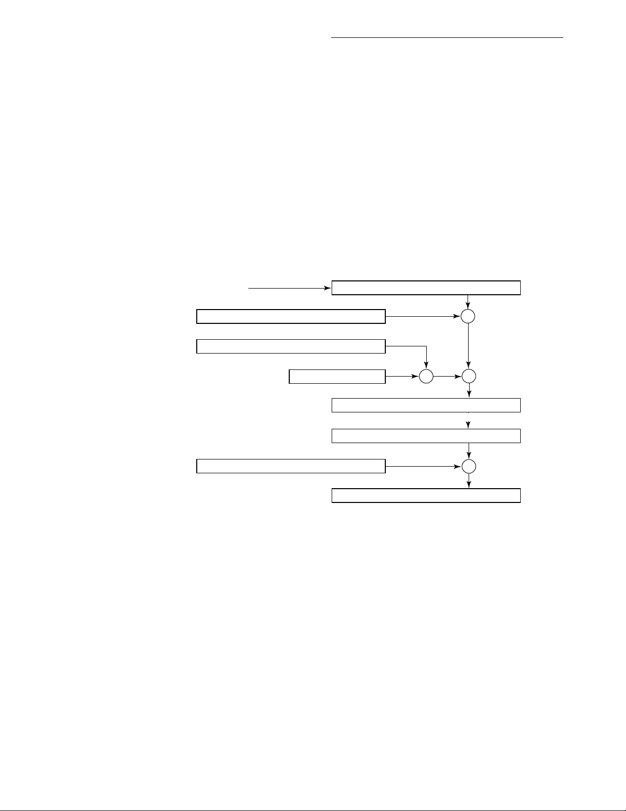
Data Organization and Addressing Capabilities
2.4.10 Memory Indirect Preindexed Mode
In this mode, the operand and its address are in memory. The processor calculates an
intermediate indirect memory address using the base register (An), a base displacement
(bd), and the index operand (Xn.SIZE * SCALE). The processor accesses a long word at
this address and adds the outer displacement to yield the effective address. Both
displacements and the index register contents are sign-extended to 32 bits.
In the syntax for this mode, brackets enclose the values used to calculate the intermediate
memory address. All four user-specified values are optional. Both the base and outer
displacements may be null, word, or long word. When a displacement is omitted or an
element is suppressed, its value is taken as zero in the effective address calculation.
GENERATION:
ASSEMBLER SYNTAX:
MODE:
ADDRESS REGISTER:
31 0
BASE DISPLACEMENT:
EA = (bd + An + Xn.SIZE*SCALE) + od
([bd,An,Xn.SIZE*SCALE],od)
110
An
SIGN-EXTENDED VALUE
31 0
MEMORY ADDRESS
+
31 0
SIGN-EXTENDED VALUE
7
INDEX REGISTER:
SCALE:
31 0
OUTER DISPLACEMENT:
EFFECTIVE ADDRESS:
NUMBER OF EXTENSION WORDS: 1,2, 3, 4, OR 5
SIGN-EXTENDED VALUE
0
SCALE VALUE
31 0
INDIRECT MEMORY ADDRESS
31 0
VALUE AT INDIRECT MEMORY ADDRESS
X
+
POINTS TO
+
31 0
OPERAND
MOTOROLA
MC68030 USER’S MANUAL
2-15
Page 54

Data Organization and Addressing Capabilities
2.4.11 Program Counter Indirect with Displacement Mode
In this mode, the operand is in memory. The address of the operand is the sum of the
address in the PC and the sign-extended 16-bit displacement integer in the extension word.
The value in the PC is the address of the extension word. The reference is a program space
reference and is only allowed for reads (refer to 4.2 Address Space Types ).
GENERATION:
ASSEMBLER SYNTAX:
MODE:
REGISTER:
PROGRAM COUNTER:
DISPLACEMENT: INTEGER
MEMORY ADDRESS:
NUMBER OF EXTENSION WORDS: 1
SIGN EXTENDED
EA = (PC) + d
d ,PC)
16
111
010
15
16
31 0
ADDRESS OF EXTENSION WORD
031
+
31 0
OPERAND
2.4.12 Program Counter Indirect with Index (8-Bit Displacement) Mode
This mode is similar to the address register indirect with index (8-bit displacement) mode
described in 2.4.7 Address Register Indirect with Index (8-Bit Displacement) Mode , but
the PC is used as the base register. The operand is in memory. The address of the operand
is the sum of the address in the PC, the sign-extended displacement integer in the lower
eight bits of the extension word, and the sized, scaled, and sign-extended index operand.
The value in the PC is the address of the extension word. This reference is a program space
reference and is only allowed for reads. The user must include the displacement, the PC,
and the index register when specifying this addressing mode.
GENERATION:
ASSEMBLER SYNTAX:
MODE:
REGISTER:
PROGRAM COUNTER:
31 0
DISPLACEMENT:
31 0
INDEX REGISTER
SCALE:
NUMBER OF EXTENSION WORDS:
EA = (PC) + (Xn) + d
(d , PC,Xn. SIZE*SCALE)
111
011
SIGN EXTENDED
SIGN-EXTENDED VALUE
8
8
31 0
ADDRESS OF EXTENSION WORD
7
INTEGER
70
SCALE VALUE
31 0
1
X
OPERANDMEMORY ADDRESS:
+
+
2-16
MC68030 USER’S MANUAL
MOTOROLA
Page 55

Data Organization and Addressing Capabilities
2.4.13 Program Counter Indirect with Index (Base Displacement) Mode
This mode is similar to the address register indirect with index (base displacement) mode
described in 2.4.8 Address Register Indirect with Index (Base Displacement) Mode , but
the PC is used as the base register. It requires an index register indicator and an optional
16- or 32-bit sign-extended base displacement. The operand is in memory. The address of
the operand is the sum of the contents of the PC, the scaled contents of the sign-extended
index register, and the base displacement. The value of the PC is the address of the first
extension word. The reference is a program space reference and is only allowed for reads
(refer to 4.2 Address Space Types ).
In this mode, the PC, the index register, and the displacement are all optional. However, the
user must supply the assembler notation "ZPC'' (zero value is taken for the PC) to indicate
that the PC is not used. This allows the user to access the program space without using the
PC in calculating the effective address. The user can access the program space with a data
register indirect access by placing ZPC in the instruction and specifying a data register (Dn)
as the index register.
GENERATION:
ASSEMBLER SYNTAX:
MODE:
REGISTER:
PROGRAM COUNTER:
31 0
BASE DISPLACEMENT:
31 0
INDEX REGISTER
SCALE:
NUMBER OF EXTENSION WORDS:
EA = (PC) + (Xn) + bd
(bd, PC, Xn. SIZE*SCALE)
111
011
SIGN-EXTENDED VALUE
SIGN-EXTENDED VALUE
1, 2 OR 3
31 0
SCALE VALUE
31 0
ADDRESS OF EXTENSION WORD
+
07
X
OPERANDMEMORY ADDRESS:
+
MOTOROLA
MC68030 USER’S MANUAL
2-17
Page 56

Data Organization and Addressing Capabilities
2.4.14 Program Counter Memory Indirect Postindexed Mode
This mode is similar to the memory indirect postindexed mode described in 2.4.9 Memory
Indirect Postindexed Mode, but the PC is used as the base register. Both the operand and
operand address are in memory. The processor calculates an intermediate indirect memory
address by adding a base displacement (bd) to the PC contents. The processor accesses a
long word at that address and adds the scaled contents of the index register and the optional
outer displacement (od) to yield the effective address. The value of the PC used in the
calculation is the address of the first extension word. The reference is a program space
reference and is only allowed for reads (refer to 4.2 Address Space Types).
In the syntax for this mode, brackets enclose the values used to calculate the intermediate
memory address. All four user-specified values are optional. However, the user must supply
the assembler notation ZPC (zero value is taken for the PC) to indicate that the PC is not
used. This allows the user to access the program space without using the PC in calculating
the effective address. Both the base and outer displacements may be null, word, or long
word. When a displacement is omitted or an element is suppressed, its value is taken as
zero in the effective address calculation.
GENERATION:
ASSEMBLER SYNTAX:
MODE:
REGISTER FIELD:
PROGRAM COUNTER:
31
BASE DISPLACEMENT:
31 0
INDEX REGISTER:
31 0
OUTER DISPLACEMENT:
EFFECTIVE ADDRESS:
NUMBER OF EXTENSION WORDS: 1,2, 3, 4, OR 5
EA = (bd + PC) + Xn.SIZE*SCALE + od
([bd, PC], Xn.SIZE*SCALE,od)
111
011
SIGN-EXTENDED VALUE
SIGN-EXTENDED VALUE
SIGN-EXTENDED VALUE
31 0
MEMORY ADDRESS
0
+
31 0
INDIRECT MEMORY ADDRESS
X
POINTS TO
+
31 0
VALUE AT INDIRECT MEMORY
ADDRESS IN PROGRAM SPACE
07
SCALE VALUE
+
31 0
OPERAND
2-18 MC68030 USER’S MANUAL MOTOROLA
Page 57

Data Organization and Addressing Capabilities
2.4.15 Program Counter Memory Indirect Preindexed Mode
This mode is similar to the memory indirect preindexed mode described in 2.4.10 Memory
Indirect Preindexed Mode, but the PC is used as the base register. Both the operand and
operand address are in memory. The processor calculates an intermediate indirect memory
address by adding the PC contents, a base displacement (bd), and the scaled contents of
an index register. The processor accesses a long word at that address and adds the optional
outer displacement (od) to yield the effective address. The value of the PC is the address of
the first extension word. The reference is a program space reference and is only allowed for
reads (refer to 4.2 Address Space Types).
In the syntax for this mode, brackets enclose the values used to calculate the intermediate
memory address. All four user-specified values are optional. However, the user must supply
the assembler notation ZPC (zero value is taken for the PC) to indicate that the PC is not
used. This allows the user to access the program space without using the PC in calculating
the effective address. Both the base and outer displacements may be null, word, or long
word. When a displacement is omitted or an element is suppressed, its value is taken as
zero in the effective address calculation.
GENERATION:
ASSEMBLER SYNTAX:
MODE:
REGISTER FIELD:
PROGRAM COUNTER:
31 0
BASE DISPLACEMENT:
31 0
INDEX REGISTER
31 0
OUTER DISPLACEMENT:
NUMBER OF EXTENSION WORDS:
EA = (bd + PC + Xn . SIZE * SCALE) + od
([bd, PC, Xn. SIZE*SCALE],od)
111
011
SIGN-EXTENDED VALUE
SIGN-EXTENDED VALUE
7
SIGN-EXTENDED VALUE
1, 2, 3, 4 OR 5
31 0
ADDRESS OF EXTENSION WORD
0
SCALE VALUE
31 0
INDIRECT MEMORY ADDRESS
31 0
VALUE AT INDIRECT MEMORY
ADDRESS IN PROGRAM SPACE
31 0
+
X
+
POINTS TO
+
OPERANDEFFECTIVE ADDRESS:
MOTOROLA MC68030 USER’S MANUAL 2-19
Page 58

Data Organization and Addressing Capabilities
2.4.16 Absolute Short Addressing Mode
In this addressing mode, the operand is in memory, and the address of the operand is in the
extension word. The 16-bit address is sign-extended to 32 bits before it is used.
GENERATION:
ASSEMBLER SYNTAX:
MODE:
REGISTER FIELD:
EXTENSION WORD:
MEMORY ADDRESS:
NUMBER OF EXTENSION WORDS: 1
EA GIVEN
(xxx).W
111
000
31 0
31 0
15
MEMORY ADDRESSSIGN EXTENDED
OPERAND
2.4.17 Absolute Long Addressing Mode
In this mode, the operand is in memory, and the address of the operand occupies the two
extension words following the instruction word in memory. The first extension word contains
the high-order part of the address; the low-order part of the address is the second extension
word.
GENERATION:
ASSEMBLER SYNTAX:
MODE:
REGISTER FIELD:
FIRST EXTENSION WORD:
SECOND EXTENSION WORD:
MEMORY ADDRESS:
NUMBER OF EXTENSION WORDS:
EA GIVEN
(xxx).L
111
001
2
15
ADDRESS HIGH
31 0
31 0
0
15
ADDRESS LOW
CONCATENATION
OPERAND
0
2-20 MC68030 USER’S MANUAL MOTOROLA
Page 59

Data Organization and Addressing Capabilities
2.4.18 Immediate Data
In this addressing mode, the operand is in one or two extension words:
Byte Operation
Operand is in the low-order byte of the extension word
Word Operation
Operand is in the extension word
Long-Word Operation
The high-order 16 bits of the operand are in the first extension word; the low-order 16
bits are in the second extension word.
Coprocessor instructions can support immediate data of any size. The instruction word is
followed by as many extension words as are required.
Generation: Operand given
Assembler Syntax: #xxx
Mode Field: 111
Register Field: 100
Number of Extension Words: 1 or 2, except for coprocessor instructions
MOTOROLA MC68030 USER’S MANUAL 2-21
Page 60

Data Organization and Addressing Capabilities
2.5 EFFECTIVE ADDRESS ENCODING SUMMARY
Most of the addressing modes use one of the three formats shown in Figure 2–4. The single
effective address instruction is in the format of the instruction word. The encoding of the
mode field of this word selects the addressing mode. The register field contains the general
register number or a value that selects the addressing mode when the mode field contains
"111.'' Table 2–2 shows the encoding of these fields. Some indexed or indirect modes use
the instruction word followed by the brief format extension word. Other indexed or indirect
modes consist of the instruction word and the full format of extension words. The longest
instruction for the MC68030 contains 10 extension words. It is a MOVE instruction with full
format extension words for both source and destination effective addresses and with 32-bit
base displacements and 32-bit outer displacements for both addresses. However,
coprocessor instructions can have any number of extension words. Refer to the coprocessor
instruction formats in Section 10 Coprocessor Interface Description.
For effective addresses that use the full format, the index suppress (IS) bit and the index/
indirect selection (I/IS) field determine the type of indexing and indirection. Table 2–1 lists
the indexing and indirection operations corresponding to all combinations of IS and I/IS
values.
Table 2-1. IS–I/IS Memory Indirection Encodings
IS Index/Indirect Operation
0 000 No Memory Indirection
0 001 Indirect Preindexed with Null Outer Displacement
0 010 Indirect Preindexed with Word Outer Displacement
0 011 Indirect Preindexed with Long Outer Displacement
0 100 Reserved
0 101 Indirect Postindexed with Mull Outer Displacement
0 110 Indirect Postindexed with Word Outer Displacement
0 111 Indirect Postindexed with Long Outer Displacement
1 000 No Memory Indirection
1 001 Memory Indirect with Mull Outer Displacement
1 010 Memory Indirect with Word Outer Displacement
1 011 Memory Indirect with Long Outer Displacement
1 100–111 Reserved
2-22 MC68030 USER’S MANUAL MOTOROLA
Page 61

Data Organization and Addressing Capabilities
Single Effective Address Instruction Format
15 14 13 12 11 10 9 8 7 6 5 0
X X X X X X X X X X
Brief Format Extension Word
15 14 12 11 10 9 8 7 0
D/A REGISTER W/L SCALE 0 DISPLACEMENT
Full Format Extension Word(s)
15 14 12111098765432 0
D/A REGISTER W/L SCALE 1 BS IS BD SIZE 0 I/IS
BASE DISPLACEMENT (0, 1, OR 2 WORDS)
OUTER DISPLACEMENT (0, 1, OR 2 WORDS)
EFFECTIVE ADDRESS
MODE REGISTER
Field Definition Field Definition
Instruction: BS Base Register Suppress:
Register General Register Number 0 = Base Register Added
Extensions: 1 = Base Register Suppressed
Register Index Register Number IS Index Suppress:
D/A Index Register Type 0 = Evaluate and Add Index
0 = Dn Operand
1 = An 1 = Suppress Index Operand
W/L Word/Long-Word Index Size BD SIZE Base Displacement Size:
0 = Sign-Extended Word 00 = Reserved
1 = Long Word 01 = Null Displacement
Scale Scale Factor 10 = Word Displacement
00 =1 11 Long Displacement
01 =2 I/IS Index/Indirect Selection
10 = 4 Indirect and Indexing Operand
11 = 8 Determined in Conjunction with
Bit 6, Index Suppress
Figure 2-4. Effective Address Specification Formats
Effective address modes are grouped according to the use of the mode. They can be
classified as follows:
Data A data addressing effective address mode is one that refers to data operands.
Memory A memory addressing effective address mode is one that refers to memory
operands.
Alterable An alterable addressing effective address mode is one that refers to alterable
(writable) operands.
Control A control addressing effective address mode is one that refers to memory
operands without an associated size.
MOTOROLA MC68030 USER’S MANUAL 2-23
Page 62

Data Organization and Addressing Capabilities
Table 2–2 shows the categories to which each of the effective addressing modes belong.
Addressing Modes Mode Register Data Memory Control Alterable
Data Register Direct 000 reg. no. X — — X Dn
Address Register Direct 001 reg. no. — — — X An
Address Register Indirect
Address Register Indirect
with Postincrement
Address Register Indirect
with Predecrement
Address Register Indirect
with Displacement
Address Register Indirect with
Index (8-Bit Displacement)
Address Register Indirect with
Index (Base Displacement)
Memory Indirect Postindexed
Memory Indirect Preindexed
Absolute Short
Absolute Long
Program Counter Indirect
with Displacement
Program Counter Indirect
with Index (8-Bit) Displacement
Program Counter Indirect
with Index (Base Displacement)
PC Memory Indirect
Postindexed
PC Memory Indirect
Preindexed
Immediate 111 100 X X — — #〈data〉
010
011
100
101
110
110
110
110
111
111
111
111
111
111
111
reg. no
reg. no.
reg. no.
reg. no.
reg. no.
reg. no.
reg. no
reg. no.
000
001
010
011
011
011
011
X
X
X
X
X
X
X
X
X
X
X
X
X
X
X
X
X
X
X
X
X
X
X
X
X
X
X
X
X
X
—
—
X
X
X
X
X
X
X
X
X
X
X
X
X
X
X
X
X
X
X
X
X
X
X
—
—
—
—
—
Assembler
Syntax
(An)
(An)+
-(An)
,An)
(d
16
(d
,An,Xn)
8
(bd,An,Xn)
([bd,An],Xn,od)
([bd,An,Xn],od)
(xxx).W
(xxx).L
,PC)
(d
16
(d8,PC,Xn)
(bd,PC,Xn)
([bd,PC],Xn,od)
([bd,PC,Xn],od)
These categories are sometimes combined, forming new categories that are more
restrictive. Two combined classifications are alterable memory or data alterable. The former
refers to those addressing modes that are both alterable and memory addresses, and the
latter refers to addressing modes that are both data and alterable.
2.6 PROGRAMMER`S VIEW OF ADDRESSING MODES
Extensions to the indexed addressing modes, indirection, and full 32-bit displacements
provide additional programming capabilities for both the MC68020 and the MC68030. This
section describes addressing techniques that exploit these capabilities and summarizes the
addressing modes from a programming point of view.
2-24 MC68030 USER’S MANUAL MOTOROLA
Page 63

Data Organization and Addressing Capabilities
Several of the addressing techniques described in this section use data registers and
address registers interchangeably. While the MC68030 provides this capability, its
performance has been optimized for addressing with address registers. The performance of
a program that uses address registers in address calculations is superior to that of a
program that similarly uses data registers.The performance has been optimized for
addressing registers in address calculations is superior to that of a program that similarly
uses data registers. The specification of addresses with data registers should be used
sparingly (if at all), particularly in programs that require maximum performance.
2.6.1 Addressing Capabilities
In both the MC68020 and the MC68030, setting the base register suppress (BS) bit in the
full format extension word (see Figure 2–4) suppresses use of the base address register in
calculating the effective address. This allows any index register to be used in place of the
base register. Since any of the data registers can be index registers, this provides a data
register indirect form (Dn). The mode could be called register indirect (Rn) since either a
data register or an address register can be used. This addressing mode is an extension to
the M68000 Family because the MC68030 and MC68020 can use both the data registers
and the address registers to address memory. The capabilities of specifying the size and
scale of an index register (Xn.SIZE*SCALE) in these modes provides additional addressing
flexibility. Using the SIZE parameter, either the entire contents of the index register can be
used, or the least significant word can be sign-extended to provide a 32-bit index value (refer
to Figure 2–5).
D1.L
D1.W
31
0
D1
16 1531 0
D1
USED IN ADDRESS CALCULATION
Figure 2-5. Using SIZE in the Index Selection
MOTOROLA MC68030 USER’S MANUAL 2-25
Page 64

Data Organization and Addressing Capabilities
For both the MC68020 and the MC68030, the register indirect modes can be extended
further. Since displacements can be 32 bits wide, they can represent absolute addresses or
the results of expressions that contain absolute addresses. This allows the general register
indirect form to be (bd,Rn) or (bd,An,Rn) when the base register is not suppressed. Thus,
an absolute address can be directly indexed by one or two registers (refer to Figure 2–6).
SYNTAX (bd,An,Rn)
bd
An
Rn
Figure 2-6. Using Absolute Address with Indexes
Scaling provides an optional shifting of the value in an index register to the left by zero, one,
two, or three bits before using it in the effective address allocation (the actual value in the
index register remains unchanged). This is equivalent to multiplying the register by one, two,
four, or eight or direct subscripting into an array of elements of corresponding size using an
arithmetic value residing in any of the 16 general registers. Scaling does not add to the
effective address calculation time. However, when combined with the appropriate derived
modes, it produces additional capabilities. Arrayed structures can be addressed absolutely
and then subscripted, (bd,Rn*scale). Another variation that can be derived is (An,Rn*scale).
In the first case, the array address is the sum of the contents of a register and a
displacement, as shown in Figure 2–7. In the second example. An contains the address of
an array and Rn contains a subscript.
2-26 MC68030 USER’S MANUAL MOTOROLA
Page 65

Data Organization and Addressing Capabilities
SYNTAX: MOVE.W (A5, A6.L*SCALE),(A7)
WHERE:
A5 = ADDRESS OF ARRAY STRUCTURE
A6 = INDEX NUMBER OF ARRAY ITEM
A7 = STACK POINTER
A6 = 1
A6 = 1
SIMPLE ARRAY
(SCALE = 1)
2
3
4
RECORD OF 4 WORDS
(SCALE = 4)
15 0 15 0
A6 = 1
2
A6 = 1
RECORD OF 2 WORDS
(SCALE = 2)
15 015 0
RECORD OF 8 WORDS
(SCALE = 8)
2
2
NOTE: Regardless of array structure, software increments
index by the appropriate amount to point to next record.
Figure 2-7. Addressing Array Items
MOTOROLA MC68030 USER’S MANUAL 2-27
Page 66

Data Organization and Addressing Capabilities
The memory indirect addressing modes use a long-word pointer in memory to access an
operand. Any of the modes previously described can be used to address the memory
pointer. Because the base and index registers can both be suppressed, the displacement
acts as an absolute address, providing indirect absolute memory addressing (refer to Figure
2–8).
The outer displacement (od) available in the memory indirect modes is added to the pointer
in memory. The syntax for these modes is ([bd,An],Xn,od) and ([bd,An,Xn],od). When the
pointer is the address of a structure in memory and the outer displacement is the offset of
an item in the structure, the memory indirect modes can access the item efficiently (refer to
Figure 2–9).
Memory indirect addressing modes are used with a base displacement in five basic forms:
1. [bd,An] — Indirect, suppressed index register
2. ([bd,An,Xn]) — Preindexed indirect
3. ([bd,An],Xn) — Postindexed indirect
4. ([bd,An,Xn],od) — Preindexed indirect with outer displacement
5. ([bd,An],Xn,od) — Postindexed indirect with outer displacement
SYNTAX: ([bd])
bd
POINTER DATA ITEM
Figure 2-8. Using Indirect Absolute Memory Addressing
The indirect, suppressed index register mode (see Figure 2–10) uses the contents of
register An as an index to the pointer located at the address specified by the displacement.
The actual data item is at the address in the selected pointer.
The preindexed indirect mode (see Figure 2–11) uses the contents of An as an index to the
pointer list structure at the displacement. Register Xn is the index to the pointer, which
contains the address of the data item.
2-28 MC68030 USER’S MANUAL MOTOROLA
Page 67

Data Organization and Addressing Capabilities
SYNTAX: ([An],od)
MEMORY STRUCTURE
An
POINTER
od
DATA ITEM
Figure 2-9. Accessing an Item in a Structure Using a Pointer
SYNTAX: ([bd,An])
POINTER LIST
bd
An
POINTER
DATA ITEM
Figure 2-10. Indirect Addressing, Suppressed Index Register
MOTOROLA MC68030 USER’S MANUAL 2-29
Page 68

Data Organization and Addressing Capabilities
POINTER LIST
SYNTAX: ([bd,An,Xn])
bd
An
DATA ITEM
Xn
POINTER
Figure 2-11. Preindexed Indirect Addressing
2-30 MC68030 USER’S MANUAL MOTOROLA
Page 69

Data Organization and Addressing Capabilities
The postindexed indirect mode (see Figure 2–12) uses the contents of An as an index to the
pointer list at the displacement. Register Xn is used as an index to the structure of data items
located at the address specified by the pointer. Figure 2–13 shows the preindexed indirect
addressing with outer displacement mode.
SYNTAX: ([bd,An],Xn)
bd
bd
POINTER LIST
An
POINTER
POSTINDEXED STRUCTURE
Xn
DATA ITEM
Figure 2-12. Postindexed Indirect Addressing
SYNTAX: ([bd,An,Xn],od)
POINTER LIST
An
STRUCTURE
od
Xn
POINTER
DATA ITEM
Figure 2-13. Preindexed Indirect Addressing with Outer Displacement
MOTOROLA MC68030 USER’S MANUAL 2-31
Page 70

Data Organization and Addressing Capabilities
The postindexed indirect mode with outer displacement (see Figure 2–14) uses the contents
of An as an index to the pointer list at the displacement. Register Xn is used as an index to
the structure of data structures at the address in the pointer. The outer displacement (od) is
the displacement of the data item within the selected data structure.
SYNTAX: ([bd,An],Xn,od)
POINTER LIST
bd
An
POINTER
POSTINDEXED STRUCTURE
WITH OUTER DISPLACEMENT
od
Xn
DATA ITEM
Figure 2-14. Postindexed Indirect Addressing with Outer Displacement
2.6.2 General Addressing Mode Summary
The addressing modes described in the previous section are derived from specific
combinations of options in the indexing mode or a selection of two alternate addressing
modes. For example, the addressing mode called register indirect (Rn) assembles as the
address register indirect if the register is an address register. If Rn is a data register, the
assembler uses the address register indirect with index mode using the data register as the
indirect register and suppresses the address register by setting the base suppress bit in the
effective address specification. Assigning an address register as Rn provides higher
performance than using a data register as Rn. Another case is (bd,An), which selects an
addressing mode depending on the size of the displacement. If the displacement is 16 bits
or less, the address register indirect with displacement mode (d
bit displacement is required, the address register indirect with index (bd,An,Xn) is used with
the index register suppressed.
,An) is used. When a 32-
16
2-32 MC68030 USER’S MANUAL MOTOROLA
Page 71

Data Organization and Addressing Capabilities
It is useful to examine the derived addressing modes available to a programmer (without
regard to the MC68030 effective addressing mode actually encoded) because the
programmer need not be concerned about these decisions. The assembler can choose the
more efficient addressing mode to encode.
In the list of derived addressing modes that follows, common programming terms are used.
The following definitions apply:
pointer — long-Word value in a register or in memory which represents an
address.
base — A pointer combined with a displacement to represent an address.
index — A constant or variable value added into an effective address calcula-
tion. A constant index is a displacement. A variable index is always
represented by a register containing the value.
disp — Displacement, a constant index.
subscript — The use of any of the data or address registers as a variable index
subscript into arrays of items 1, 2, 4 or 8 bytes in size.
relative — An address calculated from the program counter contents. The
address is position independent and is in program space. All other
addresses but psaddr are in data space.
addr — An absolute address.
psaddr — An absolute address in program space. All other addresses but PC
relative are in data space.
preindexed — All modes from absolute address through program counter relative.
postindexed— Any of the following modes:
addr — Absolute address in data space
psaddr,ZPC — Absolute address in program space
An — Register pointer with constant displacement
disp.An — Register pointer with constant displacement
addr,An — Absolute address with single variable name
disp,Pc — Simple PC relative
The addressing modes defined in programming terms, which are derivations of the
addressing modes provided by the MC68030 architecture, are as follows:
Immediate Data — #data:
The data is a constant located in the instruction stream.
Register Direct — Rn:
The contents of a register contain the operand.
Scanning Modes:
(An)+
MOTOROLA MC68030 USER’S MANUAL 2-33
Page 72

Data Organization and Addressing Capabilities
Address register pointer automatically incremented after use.
– (An)
Address register pointer automatically decremented before use.
Absolute Address:
(addr)
Absolute address in data space.
(psaddr,ZPC)
Absolute address in program space. Symbol ZPC suppresses the PC,
but retains PC relative mode to directly access the program space.
Register Pointer:
(Rn)
Register as a pointer.
(disp,Rn)
Register as a pointer with constant index (or base address).
Indexing
(An,Rn)
Register pointer An with variable index Rn.
(disp,An,Rn)
Register pointer with constant and variable index (or a base address
with a variable index).
(addr,Rn)
Absolute address with two variable indexes.
Subscripting:
(An,Rn*scale)
Address register pointer subscript.
(disp,An,Rn*scale)
Address register pointer subscript with constant displacement
(or base address with subscript).
(addr,Rn*scale)
Absolute address with subscript.
(addr,An,Rn*scale)
Absolute address subscript with variable index.
Program Relative:
2-34 MC68030 USER’S MANUAL MOTOROLA
Page 73

(disp,PC)
Simple PC relative.
(disp,PC,Rn)
PC relative with variable index.
(disp,PC,Rn*scale)
PC relative with subscript.
Memory Pointer:
([preindexed])
Memory pointer directly to data operand.
([preindexed],disp)
Memory pointer as base with displacement to data operand.
([postindexed],Rn)
Data Organization and Addressing Capabilities
Memory pointer with variable index.
([postindexed],disp,Rn)
Memory pointer with constant and variable index.
([postindexed],Rn*scale)
Memory pointer subscripted.
([postindexed],disp,Rn*scale)
Memory pointer subscripted with constant index.
MOTOROLA MC68030 USER’S MANUAL 2-35
Page 74

Data Organization and Addressing Capabilities
2.7 M68000 FAMILY ADDRESSING COMPATIBILITY
Programs can be easily transported from one member of the M68000 Family to another in
an upward compatible fashion. The user object code of each early member of the family is
upward compatible with newer members and can be executed on the newer microprocessor
without change. The address extension word(s) are encoded with the information that allows
the MC68020/MC68030 to distinguish the new address extension words for the early
MC68000/MC68008/MC68010 microprocessors and for the newer 32-bit MC68020/
MC68030 microprocessors are shown in Figure 2–15. Notice the encoding for SCALE used
by the MC68020/MC68030 is a compatible extension of the M68000 architecture. A value
of zero for SCALE is the same encoding for both extension words; hence, software that uses
this encoding is both upward and downward compatible across all processors in the product
line. However, the other values of SCALE are not found in both extension formats; thus,
while software can be easily migrated in an upward compatible direction, only nonscaled
addressing is supported in a downward fashion. If the MC68000 were to execute an
instruction that encoded a scaling factor, the scaling factor would be ignored and not access
the desired memory address. The earlier microprocessors have no knowledge of the
extension word formats implemented by newer processors; while they do detect illegal
instructions, they do not decode invalid encodings of the extension words as exceptions.
2.8 OTHER DATA STRUCTURES
Stacks and queues are widely used data structures. The MC68030 implements a system
stack and also provides instructions that support the use of user stacks and queues.
2.8.1 System Stack
Address register seven (A7) is used as the system stack pointer (SP). Any of the three
system stack registers is active at any one time. The M and S bits of the status register
determine which stack pointer is used. When S = 0 indicating user mode (user privilege
level), the user stack pointer (USP) is the active system stack pointer, and the master and
interrupt stack pointers cannot be referenced. When S = 1 indicating supervisor mode (at
supervisor privilege level) and M = 1, the master stack pointer (MSP) is the active system
stack pointer. When S = 1 and M = 0, the interrupt stack pointer (ISP) is the active system
stack pointer. This mode is the MC68030 default mode after reset and corresponds to the
MC68000, MC68008, and MC68010 supervisor mode. The term supervisor stack pointer
(SSP) refers to the master or interrupt stack pointers, depending on the state of the M bit.
When M = 1, the term SSP (or A7) refers to the MSP address register. When M = 0, the term
is implicitly referenced by all instructions that use the system stack. Each system stack fills
from high to low memory.
2-36 MC68030 USER’S MANUAL MOTOROLA
Page 75

Data Organization and Addressing Capabilities
(UNABLE TO LOCATE ART. MUST BE RECREATED.)
Figure 2-15. M68000 Family Address Extension Words
A subroutine call saves the program counter on the active system stack, and the return
restores it from the active system stack. During the processing of traps and interrupts, both
the program counter and the status register are saved on the supervisor stack (either master
or interrupt). Thus, the execution of supervisor code is independent of user code and the
condition of the user stack; conversely, user programs use the user stack pointer
independently of supervisor stack requirements.
To keep data on the system stack aligned for maximum efficiency, the active stack pointer
is automatically decremented or incremented by two for all byte-sized operands moved to
or from the stack. In long-word-organized memory, aligning the stack pointer on a long-word
address signed significantly increases the efficiency of stacking exception frames,
subroutine calls and returns, and other stacking operations.
MOTOROLA MC68030 USER’S MANUAL 2-37
Page 76

Data Organization and Addressing Capabilities
2.8.2 User Program Stacks
The user can implement stacks with the address register indirect with postincrement and
predecrement addressing modes. With address register An (n = 0–6), the user can
implement a stack that is filled wither from high to low memory or from low to high memory.
Important considerations are:
• Use the predecrement mode to decrement the register before its contents are used as
the pointer to the stack.
• Use the postincrement mode to increment the register after its contents are used as the
pointer to the stack.
• Maintain the stack pointer correctly when byte, word, and long-word items are mixed in
these stacks.
To implement stack growth from high to low memory, use:
–(An) to push data on the stack,
(An)+ to pull data from the stack.
For this type of stack, after either a push or a pull operation, register An points to the top item
on the stack. This is illustrated as:
LOW MEMORY
An
(FREE)
TOP OF STACK
BOTTOM OF STACK
HIGH MEMORY
To implement stack growth from low to high memory, use:
(An)+ to push data on the stack,
–An to pull data from the stack.
2-38 MC68030 USER’S MANUAL MOTOROLA
Page 77

Data Organization and Addressing Capabilities
In this case, after either a push or pull operation, register An points to the next available
space on the stack. This is illustrated as:
LOW MEMORY
BOTTOM OF STACK
TOP OF STACK
An
(FREE)
HIGH MEMORY
2.8.3 Queues
The user can implement queues with the address register indirect with postincrement or
predecrement addressing modes. Using a pair of address registers (who of A0–A6), the user
can implement a queue which is filled either from high to low memory or from low to high
memory. Two registers are used because queues are pushed from one end and pulled from
the other. One register, An, contains the "put'' pointer; the other, Am, the "get'' pointer.
To implement growth of the queue from low to high memory, use:
(An)+ to put data into the queue,
(Am)+ to get data from the queue.
After a "put'' operation, the "put'' address register points to the next available space in the
queue, and the unchanged "get'' address register points to the next item to be removed from
the queue. After a "get'' operation, the "get'' address register points to the next item to be
removed from the queue, and the unchanged "put'' address register points to the next
available space in the queue. This is illustrated as:
LOW MEMORY
LAST GET (FREE)
GET (Am) +
PUT (An) +
NEXT GET
LAST PUT
(FREE)
HIGH MEMORY
To implement the queue as a circular buffer, the relevant address register should be
checked and adjusted, if necessary, before performing the "put'' or "get'' operation. The
address register is adjusted by subtracting the buffer length (in bytes) from the register.
MOTOROLA MC68030 USER’S MANUAL 2-39
Page 78

Data Organization and Addressing Capabilities
To implement growth of the queue from high to low memory, use:
–(An) to put data into the queue,
–(Am) to get data from the queue.
After a "put'' operation, the "put'' address register points to the last item place din the queue,
and the unchanged "get'' address register points to the last item removed from the queue.
After a "get'' operation, the "get'' address register points to the last item removed from the
queue, and the unchanged "put'' address register points to the last item placed in the queue.
This is illustrated as:
LOW MEMORY
(FREE)
PUT - (An)
GET - (Am)
LAST PUT
NEXT GET
LAST GET (FREE)
HIGH MEMORY
To implement the queue as a circular buffer, the "get'' or "put'' operation should be
performed first, and then the relevant address register should be checkout and adjusted, if
necessary. The address register is adjusted by adding the buffer length (in bytes) to the
register contents.
2-40 MC68030 USER’S MANUAL MOTOROLA
Page 79

SECTION 3
INSTRUCTION SET SUMMARY
This section briefly describes the MC68030 instruction set. Refer to the MC68000PM/AD,
MC68000 Programmer's Reference Manual
instruction set.
The following paragraphs include descriptions of the instruction format and the operands
used by instructions, followed by a summary of the instruction set. The integer condition
codes and floating-point details are discussed. Programming examples for selected
instructions are also presented.
, for complete details on the MC68030
3.1 INSTRUCTION FORMAT
All MC68030 instructions consist of at least one word; some have as many as 11 words (see
Figure 3–1). The first word of the instruction, called the operation word, specifies the length
of the instruction and the operation to be performed. The remaining words, called extension
words, further specify the instruction and operands. These words may be floating-point
command words, conditional predicates, immediate operands, extensions to the effective
address mode specified in the operation word, branch displacements, bit number or bit field
specifications, special register specifications, trap operands, pack/unpack constants, or
argument counts.
15 0
OPERATION WORD(ONE WORD,
SPECIFIES OPERATION AND MODES)
SPECIAL OPERAND SPECIFIERS
(IF ANY, ONE OR TWO WORDS)
IMMEDIATE OPERAND OR SOURCE EFFECTIVE ADDRESS EXTENSION(
IF ANY, ONE TO SIX WORDS)
DESTINATION EFFECTIVE ADDRESS EXTENSION
(IF ANY, ONE TO SIX WORDS)
Figure 3-1. Instruction Word General Format
MOTOROLA
MC68030 USER’S MANUAL
3-1
Page 80

Instruction Set Summary
Besides the operation code, which specifies the function to be performed, an instruction
defines the location of every operand for the function. Instructions specify an operand
location in one of three ways:
1. Register Specification — A register field of the instruction contains the number of the
register.
2. Effective Address — An effective address field of the instruction contains address
mode information.
3. Implicit Reference — The definition of an instruction implies the use of specific regis-
ters.
The register field within an instruction specifies the register to be used. Other fields within
the instruction specify whether the register selected is an address or data register and how
the register is to be used. Section 1 Introduction contains register information.
Effective address information includes the registers, displacements, and absolute
addresses for the effective address mode. Section 2 Data Organization and Addressing
Capabilities describes the effective address modes in detail.
Certain instructions operate on specific registers. These instructions imply the required
registers.
3.2 INSTRUCTION SUMMARY
The instructions form a set of tools to perform the following operations:
Data Movement
Integer Arithmetic
Logical
Shift and Rotate
Bit Manipulation
Each instruction type is described in detail in the following paragraphs
Bit Field Manipulation
Binary-Coded Decimal Arithmetic
Program Control
System Control
Multiprocessor Communications
3-2
MC68030 USER’S MANUAL
MOTOROLA
Page 81

〈 ea 〉
Instruction Set Summary
The following notations are used in this section. In the operand syntax statements of the
instruction definitions, the operand on the right is the destination operand.
An = any address register, A7–A0
Dn = any data register, D7–D0
Rn = any address or data register
CCR = condition code register (lower byte of status register)
cc = condition codes from CCR
SR = status register
SP = active stack pointer
USP = user stack pointer
ISP = supervisor/interrupt stack pointer
MSP = supervisor/master stack pointer
SSP = supervisor (master or interrupt) stack pointer
DFC = destination function code register
SFC = source function code register
Rc = control register (VBR, SFC, DFC, CACR)
= MMU control register (SRP, URP, TC, DTT0, DTT1, ITT0,
MRc
ITT1, MMUSR)
MMUSR = MMU status register
B, W, L = specifies a signed integer data type (twos complement) of
byte, word, or long word
S = single-precision real data format (32 bits)
D = double-precision real data format (64 bits)
X = extended-precision real data format (96 bits, 16 bits unused)
P = packed BCD real data format (96 bits, 12 bytes)
FPm, FPn = any floating-point data register, FP7-FP0
= floating-point system control register (FPCR, FPSR, or
PFcr
FPIAR)
k = a twos-complement signed integer (–64 to +17) that specifies
the format of a number to be stored in the packed BCD format
= displacement; d
d
is a 16-bit displacement
16
= effective address
list = list of registers, for example D3 — D0
# 〈 data 〉 = immediate data; a literal integer
{offset:width} = bit field selection
label = assemble program label
[m] = bit m of an operand
[m:n] = bits m through n of operand
MOTOROLA
MC68030 USER’S MANUAL
3-3
Page 82

÷
Λ
⊕
Instruction Set Summary
X = extend (X) bit in CCR
N = negative (N) bit in CCR
Z = Zero (Z) bit in CCR
V = overflow (V) bit in CCR
C = carry (C) bit in CCR
+ = arithmetic addition or postincrement indicator
– = arithmetic subtraction or predecrement indicator
~ = invert; operand is logically complemented
V = logical OR
Dc = data register, D7-D0 used during compare
Du = data register, D7-D0 used during update
Dr, Dq = data registers, remainder or quotient of divide
Dh, Dl = data registers, high or lo • order 32 bits of product
MSW = most significant word
LSW = least significant word
MSB = most significant bit
FC = function code
{R/W} = read or write indicator
[An] = address extensions
x = arithmetic multiplication
= arithmetic division or conjunction symbol
= logical AND
= logical exclusive OR
3.2.1 Data Movement Instructions
The MOVE instructions with their associated addressing modes are the basic means of
transferring and storing addresses and data. MOVE instructions transfer byte, word, and
long-word operands from memory to memory, memory to register, register to memory, and
register to register. Address movement instructions (MOVE or MOVEA) transfer word and
long-word operands and ensure that only valid address manipulations are executed. In
addition to the general MOVE instructions, there are several special data movement
instructions: move multiple registers (MOVEM), move peripheral data (MOVEP), move
quick (MOVEQ), exchange registers (EXG), load effective address (LEA), push effective
address (PEA), link stack (LINK), and unlink stack (UNLK).
3-4
MC68030 USER’S MANUAL
MOTOROLA
Page 83

〈 ea 〉
〈 ea 〉 , 〈 ea 〉
〈 ea 〉
〈 ea 〉 →
Instruction Set Summary
Table 3–1 is a summary of the integer and floating-point data movement operations.
Table 3-1. Data Movement Operations
Instruction Operand Syntax Operand Size Operation
EXG Rn,Rn 32 Rn ↔ Rn
LEA
LINK An,#
MOVE
MOVEA
MOVEM list,
MOVEP
MOVEQ #
PEA
UNLK An 32 An
,An 32
〈
d
〉
,An 8, 16, 32
〈
ea
〉
,list 16, 32
Dn,(d
(d
,An)
16
,An),Dn
16
〈
data
〉
,Dn 8
An
16, 32 Sp - 4 → SP; An → (SP); SP → An, SP + D → SP
source → destination
16, 32 → 32
listed registers → destination
16, 32 → 32
16, 32
→
32 immediate data → destination
32 SP — 4 → SP; 〈 ea 〉 → (SP)
source → listed registers
Dn[31:24] → (An + d); Dn[23:16] → An + d + 2);
Dn[15:8] → (An + d + 4); Dn[7:0] → (An + d + 6)
(An + d) → Dn[31:24]; (An + d + 2) → Dn[23:16];
(An + d + 4) → Dn[15:8]; (An + d + 6) → Dn[7:0]
→
SP; (SP) → An; SP + 4 → SP
3.2.2 Integer Arithmetic Instructions
The integer arithmetic operations include the four basic operations of add (ADD), subtract
(SUB), multiply (MUL), and divide (DIV) as well as arithmetic compare (CMP, CMPM,
CMP2), clear (CLR), and negate (NEG). The instruction set includes ADD, CMP, and SUB
instructions for both address and data operations with all operand sizes valid for data
operations. Address operands consist of 16 or 32 bits. The clear and negate instructions
apply to all sizes of data operands.
Signed and unsigned MUL and DIV instructions include:
• Word multiply to produce a long-word product
• Long-word multiply to produce and long-word or quad-word product
• Division of a long word divided by a word divisor (word quotient and word remainder)
• Division of a long word or quad word dividend by a long-word divisor (long-word quotient and long-word remainder)
A set of extended instructions provides multiprecision and mixed-size arithmetic. These
instructions are add extended (ADDX), subtract extended (SUBX), sign extended (EXT),
and negate binary with extend (NEGX). Refer to Table 3–2 for a summary of the integer
arithmetic operations.
MOTOROLA
MC68030 USER’S MANUAL
3-5
Page 84

Instruction Set Summary
Table 3-2. Integer Arithmetic Operations
Instruction Operand Syntax Operand Size Operation
ADD
ADDA
ADDI
ADDQ
ADDX Dn,Dn
CLR
CMP
CMPA
CMPI #
CMPM (An) +,(An) + 8, 16, 32 destination - source
CMP2
DIVS/DIVU
DIVSL/DIVUL
EXT
EXTB
MULS/MULU 〈ea〉,Dn
NEG 〈ea〉 8, 16, 32 0 - destination → destination
NEGX 〈ea〉 8, 16, 32 0 - destination - X → destination
SUB
SUBA
SUBI
SUBQ
SUBX Dn,Dn
Dn, 〈 ea 〉
〈 ea 〉 ,Dn
,An
# 〈 data 〉 , 〈 ea 〉 # 〈 data 〉 ,
–(An),–(An)
,Dn
,An
〈
data
〉
,
〈
ea
〉
,Rn 8, 16, 32 lower bound < = Rn < = upper bound
ea〉,Dn
〈ea〉,Dr:Dq
〈ea〉,Dq
〈ea〉,Dr:Dq
Dn
Dn
Dn
〈ea〉,Dl
(ea〉,Dh:Dl
〈ea〉,Dn
Dn,〈ea〉
〈ea〉,An
#〈data〉,〈ea〉
#〈data〉,〈ea〉
–(An),–(An)
8, 16, 32
8, 16, 32
16, 32
8, 16, 32
8, 16, 32
8, 16, 32
8, 16, 32
8, 16, 32 0 → destination
8, 16, 32
16, 32
8, 16, 32 destination - immediate data
32/16 → 16:16
64/32 → 32:32
32/32 → 32
32/32 → 32:32
8 → 16
16 → 32
8 → 32
16x16 → 32
32x32 → 32
32x32 → 64
8, 16, 32
8, 16, 32
16, 32
8, 16, 32
8, 16, 32
8, 16, 32
8, 16, 32
source + destination → destination
immediate data + destination → destination
source + destination + X → destination
destination - source
destination/source → destination (signed or unsigned)
sign-extended destination → destination
source y destination → destination (signed or unsigned)
destination = source → destination
destination - immediate data → destination
destination - source — X → destination
〈 ea 〉
〈 ea 〉
〈 ea 〉
〈 ea 〉
〈 ea 〉
〈 ea 〉
〈
3.2.3 Logical Instructions
The logical operation instructions (AND, OR, EOR, and NOT) perform logical operations
with all sizes of integer data operands. A similar set of immediate instructions (ANDI, ORI,
and EORI) provide these logical operations with all sizes of immediate data. The TST
instruction compares the operand with zero arithmetically, placing the result in the condition
code register. Table 3–3 summarizes the logical operations.
3-6
MC68030 USER’S MANUAL
MOTOROLA
Page 85

Instruction Set Summary
Table 3-3. Logical Operations
Instruction Operand Syntax Operand Size Operation
AND 〈ea〉,Dn
Dn,〈ea〉
ANDI #〈data〉,〈ea〉 8, 16, 32 immediate data Λ destination → destination
EOR Dn,〈data〉,〈ea〉 8, 16, 32 source ⊕ destination → destination
EORI #〈data〉,〈ea〉 8, 16, 32 immediate data x destination → destination
NOT 〈ea〉 8, 16, 32 ∼ destination → destination
OR 〈ea〉,Dn
Dn,〈ea〉
ORI #〈data〉,〈ea〉 8, 16, 32 immediate data V destination → destination
TST #〈ea〉 8, 16, 32 source — 0 to set condition codes
8, 16, 32
8, 16, 32
8, 16, 32
8, 16, 32
source Λ destination → destination
source V destination → destination
3.2.4 Shift and Rotate Instructions
The arithmetic shift instructions (ASR and ASL) and logical shift instructions (LSR and LSL)
provide shift operations in both directions. The ROR, ROL, ROXR, and ROXL instructions
perform rotate (circular shift) operations, with and without the extend bit. All shift and rotate
operations can be performed on either registers or memory.
Register shift and rotate operations shift all operand sizes. The shift count may be specified
in the instruction operation word (to shift from 1–8 places) or in a register (modulo 64 shift
count).
Memory shift and rotate operations shift word-length operands one bit position only. The
SWAP instruction exchanges the 16-bit halves of a register. Performance of shift/rotate
instructions is enhanced so that use of the ROR and ROL instructions with a shift count of
eight allows fast byte swapping. Table 3–4 is a summary of the shift and rotate operations.
MOTOROLA MC68030 USER’S MANUAL 3-7
Page 86

Instruction Set Summary
Table 3-4. Shift and Rotate Operations.
X/C
X/C 0
C
0
X/C
X/C0
C
XC
X C
MSW LSW
3.2.5 Bit Manipulation Instructions
Bit manipulation operations are accomplished using the following instructions: bit test
(BTST), bit test and set (BSET), bit test and clear (BCLR), and bit test and change (BCHG).
All bit manipulation operations can be performed on either registers or memory. The bit
number is specified as immediate data or in a data register. Register operands are 32 bits
long, and memory operands are 8 bits long. In Table 3–5, the summary of the bit
manipulation operations, Z refers to bit 2, the zero bit of the status register.
3-8 MC68030 USER’S MANUAL MOTOROLA
Page 87

Instruction Set Summary
Table 3-5. Bit Manipulation Operations
Instruction Operand Syntax Operand Size Operation
BCHG Dn,〈ea〉
#〈data〉,ea
BCLR Dn,〈ea〉
#〈data〉,ea
BSET Dn,〈ea〉
#〈data〉,〈ea〉
BTST Dn,〈ea〉
#〈data〉,ea
8, 32
8, 32
8, 32
8, 32
8, 32
8, 32
8, 32
8, 32
∼ (〈bit number〉 of destination) → Z → bit of destination
∼ (〈bit number〉 of destination) → Z;
— 0 → bit of destination
∼ (〈bit number〉 of destination) → Z;
— 1 → bit of destination
∼ (〈bit number〉 of destination) → Z
3.2.6 Bit Field Operations
The MC68030 supports variable-length bit field operations on fields of up to 32 bits. The bit
field insert (BFINS) instruction inserts a value into a bit field. Bit field extract unsigned
(BFEXTU) and bit field extract signed (BFEXTS) extract a value from the field. Bit field find
first one (BFFFO) finds the first bit that is set in a bit field. Also included are instructions that
are analogous to the bit manipulation operations; bit field test (BFTST), bit field test and set
(BFSET), bit field test and clear (BFCLR), and bit field test and change (BFCHG). Table 3–
6 is a summary of the bit field operations.
Table 3-6. Bit Field Operations
Instruction Operand Syntax Operand Size Operation
BFCHG 〈ea〉 {offset:width} 1 — 32 ∼ Field → Field
BFCLR 〈ea〉 {offset:width} 1 — 32 0's → Field
BFEXTS 〈ea〉 {offset:width},Dn 1—32 Field → Dn; Sign Extended
BFEXTU 〈ea〉 {offset:width},Dn 1 — 32 Field → Dn; Zero Extended
BFFFO 〈ea〉 {offset:width},Dn 1 — 32 Scan for first bit set in field; offset → Dn
BFINS Dn,〈ea〉 {offset:width} 1 — 32 Dn → Field
BFSET 〈ea〉 {offset:width} 1 — 32 1's → Field
BFTST 〈ea〉 {offset:width} 1 — 32 Field MSB → N; ∼ (OR of all bits in field) → Z
NOTE: All bit field instructions set the N and Z bits as shown for BFTST before performing the specified operation.
MOTOROLA MC68030 USER’S MANUAL 3-9
Page 88

Instruction Set Summary
3.2.7 Binary–coded Decimal Instructions
Five instructions support operations on binary-coded decimal (BCD) numbers. The
arithmetic operations on packed BCD numbers are add decimal with extend (ABCD),
subtract decimal with extend (SBCD), and negate decimal with extend (NBCD). PACK and
UNPACK instructions aid in the conversion of byte encoded numeric data, such as ASCII or
EBCDIC strings, to BCD data and vice versa. Table 3–7 is a summary of the BCD
operations.
Table 3-7. BCD Operations
Instruction Operand Syntax Operand Size Operation
ABCD Dn,Dn
–(An)
NBCD 〈ea〉 8 0 - destination
PACK –(An),–(An)
#〈data〉
Dn,Dn,# 〈data〉
SBCD Dn,Dn
–(An),–(An)
UNPK –(An)
#〈data〉
Dn,Dn,#〈data〉
8
8
16→8
16→8
8
8
8→16
8→16
source
unpackaged source + immediate data → packed
destination
destination
packed source → unpacked source
unpacked source + immediate data →
unpacked destination
+ destination
10
–X → destination
10
- source10 – X → destination
10
+ X → destination
10
3-10 MC68030 USER’S MANUAL MOTOROLA
Page 89

Instruction Set Summary
3.2.8 Program Control Instructions
A set of subroutine call and return instructions and conditional and unconditional branch
instructions perform program control operations. The no operation instruction (NOP) may be
used to force synchronization of the internal pipelines. Table 3–8 summarizes these
instructions.
Table 3-8. Program Control Operations
Instruction Operand Syntax Operand Size Operation
Integer and Floating-Point Conditional
Bcc 〈label〉 8, 16, 32 if condition true, then PC + d → PC
DBcc Dn,〈label〉 16 if condition false, then Dn — 1 → Dn
if Dn ≠ -1, then PC + d → PC
Scc 〈ea〉 8 if condition true, then 1's → destination;
else 0's → destination
Unconditional
BRA 〈label〉 8, 16, 32 PC + d → PC
BSR 〈label〉 8, 16, 32 SP — 4 → SP; PC→(SP); PC + d → PC
JMP 〈ea〉 none destination → PC
JSR 〈ea〉 none SP — 4 → SP; PC→ (SP); destination → PC
NOP none none PC + 2 → PC
Returns
RTD #〈d〉 16 (SP) → PC; SP + 4 + d → SP
RTR none none (SP) → CCR; SP + 2 → SP; (SP) → PC; SP + 4 → SP
RTS none none (SP) → PC; SP + 4→ SP
Letters cc in the integer instruction mnemonics Bcc, DBcc, and Scc specify testing one of the following conditions:
CC — Carry clear GE — Greater or equal
LS — Lower or same PL — Plus
CS — Carry set GT — Greater than
LT — Less than T — Always true*
EQ — Equal HI — Higher
MI — Minus VC — Overflow clear
F — Never true* LE — -Less or equal
NE — Not equal VS — Overflow set
*Not applicable to the Bcc instructions.
MOTOROLA MC68030 USER’S MANUAL 3-11
Page 90

Instruction Set Summary
3.2.9 System Control Instructions
Privileged instructions, trapping instructions, and instructions that use or modify the
condition code register (CCR) provide system control operations. Table 3–9 summarizes
these instructions. The TRAPcc instruction uses the same conditional tests as the
corresponding program control instructions. All of these instructions cause the processor to
flush the instruction pipe.
Table 3-9. System Control Operations
Instruction Operand Syntax Operand Size Operation
Privileged
ANDI #〈data〉,SR 16 immediate data Λ SR → SR
EORI #〈data〉,SR 16 immediate data x SR → SR
MOVE 〈ea〉,SR
SR,〈ea〉
MOVE USP,An
An,USP
MOVEC Rc,Rn
Rn,Rc
MOVES Rn, 〈ea〉
〈ea〉,Rn
ORI #〈data〉,SR 16 immediate data V SR → SR
RESET none none assert RESET
RTE none none (SP) → SR; SP + 2 → SP; (SP) → PC; SP + 4 → SP;
STOP #〈data〉 16 immediate data → SR; STOP
BKPT #〈data〉 none run breakpoint cycle, then trap as illegal instruction
CHK 〈ea〉,Dn 16, 32 if Dn < 0 or Dn > (ea), then CHK exception
CHK2 〈ea〉,Rn 8, 16, 32 if Rn < -lower bound or Rn > -upper bound, then CHK
ILLEGAL none none SSP — 2 → SSP; Vector Offset→ (SSP);
TRAP #〈data〉 none SSP — 2 → SSP; Format and Vector Offset→(SSP)
TRAPcc none
#〈data〉
TRAPV none none if V, then take overflow TRAP exception
ANDI #〈data〉,CCR 8 immediate data Λ CCR → CCR
EORI #〈data〉,CCR 8 immediate data ⊕ CCR → CCR
MOVE 〈ea〉,CCR
CCR,〈ea〉
ORI #〈data〉,CCR 8 immediate data V CCR → CCR
16
16
32
32
32
32
8, 16, 32 Rn → destination using DFC
Trap Generating
none
16, 32
Condition Code Register
16
16
source → SR
SR → destination
USP → An
An → USP
Rc → Rn
Rn → Rc
source using SFC → Rn
line
Restore stack according to format
exception
SSP — 4 → SSP; PC→ (SSP);
SSP — 2 → SSP; SR→ (SSP);
Illegal Instruction Vector Address → PC
SSP — 4 → SSP; PC→(SSP); SSP — 2 → SSP;
SR→(SSP); Vector Address → PC
if cc true, then TRAP exception
source → CCR
CCR → destination
3-12 MC68030 USER’S MANUAL MOTOROLA
Page 91

Instruction Set Summary
3.2.10 Memory Management Unit Instructions
The PFLUSH instructions flush the address translation caches (ATCs) and can optionally
select only nonglobal entries for flushing. PTEST performs a search of the address
translation tables, storing results in the MMU status register and loading the entry into the
ATC. Table 3–10 summarizes these instructions.
Table 3-10. MMU Instructions
Instruction Operand Syntax Operand Size Operation
PFLUSHA none none Invalidate all ATC entries
PFLUSHA.N none none Invalidate all nonglobal ATC entries
PFLUSH (An) none Invalidate ATC entries at effective address
PFLUSH.N (An) none Invalidate nonglobal ATC entries at effective address
PTEST (An) none Information about logical address → MMU status register
3.2.11 Multiprocessor Instructions
The TAS, CAS, and CAS2 instructions coordinate the operations of processors in
multiprocessing systems. These instructions use read-modify-write bus cycles to ensure
uninterrupted updating of memory. Coprocessor instructions control the coprocessor
operations. Table 3–11 lists these instructions.
Table 3-11. Multiprocessor Operations (Read-Modify-Write)
Instruction Operand Syntax Operand Size Operation
Read-Modify-Write
CAS Dc,Du,〈ea〉 8, 16, 32 destination — Dc → CC; if Z then Du → destination
else destination→Dc
CAS2 Dc1:Dc2,Du1:Du2,(
Rn):(Rn)
TAS 〈ea〉 8 destination — 0; set condition codes; 1 → destination [7]
cpBcc 〈label〉 16, 32 if cpcc true, then PC + d → PC
cpDBcc label,Dn 16 if cpcc false then Dn –1 → Dn
cpGEN User Defined User Defined operand → coprocessor
cpRESTORE 〈ea〉 none restore coprocessor state from 〈ea〉
cpSAVE 〈ea〉 none save coprocessor state at 〈ea〉
cpScc 〈ea〉 8 if cpcc true, then 1's → destination; else 0's → destination
cpTRAPcc none
#〈data〉
8, 16, 32 dual operand CAS
Coprocessor
if Dn ≠ –1, then PC + d → PC
none
16, 32
if cpc true, then TRAPcc exception
MOTOROLA MC68030 USER’S MANUAL 3-13
Page 92

Instruction Set Summary
3.3 INTEGER CONDITION CODES
The CCR portion of the SR contains five bits which indicate the results of many integer
instructions. Program and system control instructions use certain combinations of these bits
to control program and system flow.
The first four bits represent a condition resulting from a processor operation. The X bit is an
operand for multiprecision computations; when it is used, it is set to the value of the C bit.
The carry bit and the multiprecision extend bit are separate in the M68000 Family to simplify
programming techniques that use them (refer to Table 3–8 as an example).
The condition codes were developed to meet two criteria:
• Consistency across instructions, uses, and instances
• Meaningful Results no change unless it provides useful information
Consistency across instructions means that all instructions that are special cases of more
general instructions affect the condition codes in the same way. Consistency across
instances means that all instances of an instruction affect the condition codes in the same
way. Consistency across uses means that conditional instructions test the condition codes
similarly and provide the same results, regardless of whether the condition codes are set by
a compare, test, or move instruction.
In the instruction set definitions, the CCR is shown as follows:
XNZVC
where:
X (extend)
Set to the value of the C bit for arithmetic operations. Otherwise not affected or set to
a specified result.
N (negative)
Set if the most significant bit of the result is set. Cleared otherwise.
Z (zero)
Set if the result equals zero. Cleared otherwise.
V (overflow)
Set if arithmetic overflow occurs. This implies that the result cannot be represented in
the operand size. Cleared otherwise.
C (carry)
Set if a carry out of the most significant bit of the operand occurs for an addition. Also
set if a borrow occurs in a subtraction. Cleared otherwise.
3-14 MC68030 USER’S MANUAL MOTOROLA
Page 93

Instruction Set Summary
3.3.1 Condition Code Computation
Most operations take a source operand and a destination operand, compute, and store the
result in the destination location. Single-operand operations take a destination operand,
compute, and store the result in the destination location. Table 3–12 lists each instruction
and how it affects the condition code bits.
Table 3-12. Condition Code Computations (Sheet 1 of 2)
Operations X N Z V C Special Definition
ABCD * U ? U ? C =-Decimal Carry
Z =-Z Λ Rm Λ . . . Λ R0
ADD, ADDI, ADDQ * * * ? ? V = Sm Λ Dm Λ Rm V Sm Λ Dm Λ Rm
C = Sm Λ Dm V Rm Λ Dm V Sm Λ Rm
ADDX * * ? ? ? V = Sm Λ Dm Λ Rm V Sm Λ Dm Λ Rm
C = Sm Λ Dm V Rm Λ Dm V Sm Λ Rm
Z = Z Λ Rm
AND, ANDI, EOR, EORI,
MOVEQ, MOVE, OR, ORI
CLR, EXT, NOT, TAS, TST
CHK — * U U U
CHK2, CMP2 — U ? U ? Z = (R = LB) V (R = UB)
SUB, SUBI, SUBQ * * * ? ? V = Sm Λ Dm
SUBX * * ? ? ? V = Sm Λ Dm Λ Rm V Sm Λ Dm Λ Rm
CAS, CAS2, CMP, CMPI,
CMPM
DIVS, DUVI — * * ? 0 V = Division Overflow
MULS, MULU — * * ? 0 V = Multiplication Overflow
SBCD, NBCD * U U ? C = Decimal Borrow
NEG * * * ? ? V = Dm Λ Rm
NEGX * * ? ? ? V = Dm Λ Rm
— * * 0 0
C = (LB < = UB) Λ (IR < LB) V (R > UB))
V = (UB <LB) Λ (R >UB) Λ (R <LB)
C = Sm Λ Dm V Rm Λ Dm V Sm Λ Rm
C = Sm Λ Dm V Rm Λ Dm V Sm Λ Rm
Z = Z Λ Rm Λ . . . Λ R0
— * * ? ? V = Sm Λ Dm Λ Rm V Sm Λ Dm Λ Rm
C = Sm Λ Dm V Rm Λ Dm V Sm Λ Rm
Z = Z Λ Rm
C = Dm V Rm
C = Dm V Rm
Z = Z Λ Rm Λ . . . Λ R0
Λ . . . Λ R0
Λ Rm V Sm Λ Dm Λ Rm
Λ . . . Λ R0
MOTOROLA MC68030 USER’S MANUAL 3-15
Page 94

Instruction Set Summary
Table 3-12. Condition Code Computations (Continued)
Operations X N Z V C Special Definition
BTST, BCHG, BSET, BCLR — — ? — — Z = Dn
BFTST, BFCHG, BFSET,
BFCLR
BFEXTS, BFEXTU, BFFFO — ? ? 0 0 N = Sm
BFINS — ? ? 0 0 N = Dm
ASL * * * V = Dm Λ (Dm –1 V . . . V Dm –r) V Dm Λ
ASL (R = 0) * * 0 0
LSL, ROXL * * * 0 ? C = Dm –r + 1
LSR (r = 0) — * * 0 0
ROXL (r = 0) — * * 0 ? C = X
ROL — * * 0 ? C = Dm –r + 1
ROL (r = 0) — * * 0 0
ASR, LSR, ROXR * * * 0 ? C = Dr –1
ASR, LSR (r = 0) — * * 0 0
ROXR (r = 0) — * * 0 ? C = X
ROR — * * 0 ? C = Dr –1
ROR (r = 0) — * * 0 0
— = Not Affected Rm = Result Operand — Most Significant Bit
U = Undefined, Result Meaningless R = Register Tested
? = Other — See Special Definition n = Bit Number
* = General Case r = Shift Count
X = C LB = Lower Bound
N = Rm UB = Upper Bound
Z = Rm
Λ . . . Λ R0 Λ = Boolean AND
Sm = Destination Operand — Most Significant Bit V = Boolean OR
Dm = Destination Operand — Most Significant Bit Rm
— ? ? 0 0 N = Dm
Z = Dm
Z = Sm
Z = Dm
(Dm
C = Dm –r + 1
Λ DM –1 Λ . . . Λ D0
Λ Sm –1 Λ . . . Λ S0
Λ DM–1 Λ . . . Λ D0
–1 V . . . + Dm –r)
= NOT Rm
3-16 MC68030 USER’S MANUAL MOTOROLA
Page 95

Instruction Set Summary
3.3.2 Conditional Tests
Table 3–13 lists the condition names, encodings, and tests for the conditional branch and
set instructions. The test associated with each condition is a logical formula using the current
states of the condition codes. If this formula evaluates to one, the condition is true. If the
formula evaluates to zero, the condition is false. For example, the T condition is always true,
and the EQ condition is true only if the Z bit condition code is currently true.
Table 3-13. Conditional Tests
Mnemonic Condition Encoding Test
T* True 0000 1
F* False 0001 0
HI High 0010 C
LS Low or Same 0011 C + Z
CC(HS) Carry Clear 0100 C
CS(LO) Carry Set 0101 C
NE Not Equal 0110 Z
EQ Equal 0111 Z
VC Overflow Clear 1000 V
VS Overflow Set 1001 V
PL Plus 1010 N
MI Minus 1011 N
GE Greater or Equal 1100 N •V + N
LT Less Than 1101 N •V + N •V
GT Greater Than 1110 N •V •Z
LE Less or Equal 1111 Z + N •V + N • V
• = Boolean AND
+ = Boolean OR
N
= Boolean NOT N
*Not available for the Bcc instruction.
•Z
•V
+ N • V •Z
MOTOROLA MC68030 USER’S MANUAL 3-17
Page 96

Instruction Set Summary
3.4 INSTRUCTION SET SUMMARY
Table 3–14 provides a alphabetized listing of the MC68030 instruction set listed by opcode,
operation, and syntax.
Table 3–14 use notational conventions for the operands, the subfields and qualifiers, and
the operations performed by the instructions. In the syntax descriptions, the left operand is
the source operand, and the right operand is the destination operand. The following list
contains the notations used in Table 3–14.
Notation for operands:
PC — Program counter
SR — Status register
V — Overflow condition code
Immediate Data — Immediate data from the instruction
Source — Source contents
Destination — Destination contents
Vector — Location of exception vector
+ inf — Positive infinity
–inf — Negative infinity
〈fmt〉 — Operand data format: byte (B) word (W), long
(L), single (S), double (D), extended (X), or
packed (P)
FPm — One of eight floating-point data registers (always
specifies the source register)
FPn — One of eight floating-point data registers (always
specifies the destination register)
Notation for subfields and qualifiers:
〈bit〉 of (operand〉
— Selects a single bit of the operand
〈ea〉 {offset:width} — Selects a bit field
(〈operand〉) — The contents of the referenced location
〈operand〉
— The operand is binary-coded decimal; operations are per-
10
formed in decimal
(〈address register〉) — The register indirect operation
–(〈address register〉) — Indicates that the operand register points to the memory
(〈address register〉) + — Location of the instruction operand — the optional mode
qualifiers are -, +, (d), and (d,ix)
#xxx or #〈data〉 — Immediate data that follows the instruction word(s)
3-18 MC68030 USER’S MANUAL MOTOROLA
Page 97

Instruction Set Summary
Notations for operations that have two operands, written 〈operand〉 〈op〉 〈operand〉 , where
〈op〉 is one of the following:
→ — The source operand is moved to the destination operand
↔ — The two operands are exchanged
+ — The operands are added
– — The destination operand is subtracted from the source
operand
x — The operands are multiplied
÷ — The source operand is divided by the destination operand
< — Relational test, true if source operand is less than destina-
tion operand
> — Relational test, true if source operand is greater than des-
tination operand
V — Logical OR
⊕ — Logical exclusive OR
Λ — Logical AND
shifted by, rotated by — The source operand is shifted or rotated by the number of
positions specified by the second operand
Notation for single-operand operations:
— The operand is logically complemented
〈operand〉
~〈operand〉
sign-extended— The operand is sign extended; all bits of the upper portion
are made equal to the high-order bit of the lower portion
〈operand〉
tested — The operand is compared to zero and the condition codes
are set appropriately
Notation for other operations:
TRAP — Equivalent to Format/Offset Word
→ SSP; PC→ (SSP); SSP – 4 → SSP; SR→ (SSP);
SSP–2
→ SSP; (vector) → PC
→ (SSP); SSP –2
STOP — Enter the stopped state, waiting for the interrupts
If 〈condition〉 then — The condition is tested. If true, the operations
〈operations〉 else — after "then'' are performed. If the condition is
〈operations〉 — false and the optional "else'' clause is present, the opera-
tions after "else" are performed. If the condition is false and
else is omitted, the instruction performs no operation. Refer
to the Bcc instruction description as an example.
MOTOROLA MC68030 USER’S MANUAL 3-19
Page 98

Instruction Set Summary
Table 3-14. Instruction Set Summary (Sheet 1 of 5)
Opcode Operation Syntax
ABCD Source
ADD Source + Destination → -Destination ADD 〈ea〉,Dn
ADDA Source + Destination → Destination ADDA 〈ea〉,An
ADDI Immediate Data + Destination → Destination ADDI #〈data〉,〈ea〉
ADDQ Immediate Data + Destination → Destination ADDQ #〈data〉,〈ea〉
ADDX Source + Destination + X → Destination ADDX Dy,Dx
AND Source Λ Destination → Destination AND 〈ea〉,Dn
ANDI Immediate Data Λ Destination → Destination ANDI #〈data〉,〈ea〉
ANDI
to CCR
ANDI
to SR
ASL,ASR Destination Shifted by 〈count〉 → Destination ASd Dx,Dy
Bcc If (condition true) then PC + d → PC Bcc (label〉
BCHG ∼ (〈number〉 of Destination) → Z;
BCLR ∼ (〈bit number〉 of Destination) → Z;
BFCHG ∼ (〈bit field〉 of Destination) → 〈bit field〉 of Destination BFCHG 〈ea〉{offset:width}
BFCLR 0 → 〈bit field〉 of Destination BFCLR 〈ea〉{offset:width}
BFEXTS 〈bit field〉 of Source → Dn BFEXTS 〈ea〉{offset:width},Dn
BFEXTU (bit offset〉 of Source → Dn BFEXTU 〈ea〉{offset:width},Dn
BFFFO (bit offset〉 of Source Bit Scan → Dn BFFFO 〈ea〉{offset:width},Dn
BFINS Dn → 〈bit field〉 of Destination BFINS Dn,〈ea〉{offset:width}
BFSET 1s → 〈bit field〉 of Destination BFSET 〈ea〉{offset:width}
BFTST 〈bit field〉 of Destination BFTST 〈ea〉{offset:width}
BKPT Run breakpoint acknowledge cycle;
BRA PC + d → PC BRA (label〉
BSET ~ (〈bit number〉 of Destination) → Z;
BSR SP – 4 → SP; PC → (SP); PC + d → PC BSR (label〉
BTST –(〈bit number〉 of Destination) → Z; BTST Dn,〈ea〉BTST #〈data〉,〈ea〉
Source Λ CCR → CCR ANDI #〈data〉,CCR
If supervisor state
else TRAP
∼ (〈number〉 of Destination) → 〈bit number〉 of Destination
0 → 〈bit number〉 of Destination
TRAP as illegal instruction
1 → 〈bit number〉 of Destination
+ Destination10 + X → Destination ABCD Dy,Dx
10
then Source Λ SR → SR
ABCD –(Ay),–(Ax)
ADD Dn,〈ea〉
ADDX –(Ay),–(Ax)
AND Dn,〈ea〉
ANDI #〈data〉,SR
ASd #〈data〉,Dy
ASd 〈ea〉
BCHG Dn,〈ea〉BCHG #〈data〉,〈ea〉
BCLR Dn,〈ea〉BCLR #〈data〉,〈ea〉
BKPT # 〈data〉
BSET Dn,〈ea〉BSET #〈data〉,〈ea〉
3-20 MC68030 USER’S MANUAL MOTOROLA
Page 99

Instruction Set Summary
Table 3-14. Instruction Set Summary (Sheet 2 of 5)
Opcode Operation Syntax
CAS
CAS2
CHK If Dn < 0 or >-Source then TRAP CHK 〈ea〉,Dn
CHK2 If Rn < lower bound or
CLR 0 → Destination CLR 〈ea〉
CMP Destination — Source → cc CMP 〈ea〉,Dn
CMPA Destination — Source CMPA 〈ea〉,An
CMPI Destination — Immediate Data CMPI #〈data〉,〈ea〉
CMPM Destination — Source → cc CMPM (Ay) +,(Ax) +
CMP2 Compare Rn < lower-bound or
cpBcc If cpcc true then scanPC + d → PC cpBcc (label〉
cpDBcc If cpcc false then (Dn –1 → Dn;
cpGEN Pass Command Word to Coprocessor cpGEN (parameters as defined by
cpRESTORE If supervisor state
cpSAVE If supervisor state
cpScc If cpcc true then 1s → Destination
cpTRAPcc If cpcc true then TRAP cpTRAPcc
DBcc If condition false then (Dn–1 → Dn;
DIVS
DIVSL
DIVU
DIVUL
EOR Source ⊕ Destination → Destination EOR Dn,〈ea〉
EORI Immediate Data ⊕ Destination → Destination EORI #〈data〉,〈ea〉
CAS Destination Compare Operand → cc;
if Z, Update Operand → Destination
else Destination → Compare Operand
CAS2 Destination 1 Compare 1 → cc;
if Z, Destination 2 Compare → cc;
if Z, Update 1 → Destination 1; Update 2 → Destination 2
else Destination 1 → Compare 1; Destination 2 →Compare 2
Rn > upper bound
then TRAP
Rn > upper-bound
and Set Condition Codes
if Dn ≠ –1 then scanPC + d → PC
then Restore Internal State of Coprocessor
else TRAP
the Save Internal State of Coprocessor
else TRAP
else 0s → Destination
If Dn ≠ –1 then PC + d → PC)
Destination/Source → Destination DIVS.W 〈ea〉,Dn32/16 → 16r:16q
Destination/Source → Destination DIVU.W 〈ea〉,Dn32/16 → 16r:16q
CAS Dc,Du,〈ea〉CAS2
Dc1:Dc2,Du1:Du2,(Rn1):(Rn2)
CHK2 〈ea〉,Rn
CMP2 〈ea〉,Rn
cpDBcc Dn,(label〉
coprocessorL
cpRESTORE 〈ea〉
cpSAVE 〈save〉
cpTRAPcc #〈data〉
DBcc Dn,(label〉
DIVS.L 〈ea〉,Dq 32/32 → 32q
DIVS.L 〈ea〉,Dr:Dq 64/32 → 32r:32q
DIVSL.L 〈ea〉,Dr:Dq32/32 → 32r:32q
DIVU.L 〈ea〉,Dq 32/32 → 32q
DIVU.L 〈ea〉,Dr:Dq 64/32 → 32r:32q
DIVUL.L 〈ea〉,Dr:Dq32/32 → 32r:32q
MOTOROLA MC68030 USER’S MANUAL 3-21
Page 100

Instruction Set Summary
Table 3-14. Instruction Set Summary (Sheet 3 of 5)
Opcode Operation Syntax
EORI
to CCR
EORI
to SR
EXG Rx ↔ Ry EXG Dx,Dy
EXT
EXTB
ILLEGAL SSP–2 → SSP; Vector Offset → (SSP);
JMP Destination Address → PC JMP 〈ea〉
JSR SP–4 → SP; PC → (SP)
LEA 〈ea〉 → An LEA 〈ea〉,An
LINK SP — 4 → SP; An → (SP)
LSL,LSR Destination Shifted by 〈count〉 → Destination
MOVE Source → Destination MOVE 〈ea〉,〈ea〉
MOVEA Source → Destination MOVEA 〈ea〉,An
MOVE
from CCR
MOVE
to CCR
MOVE
from SR
MOVE
to SR
MOVE
USP
MOVEC If supervisor state
MOVEM Registers → Destination
MOVEP Source → Destination MOVEP Dx,(d,Ay)
MOVEQ Immediate Data → Destination MOVEQ #〈data〉,Dn
Source ⊕ CCR → CCR EORI #〈data〉,CCR
If supervisor state
EORI #〈data〉,SR
then Source ⊕ SR → SR
else TRAP
EXG Ax,Ay
EXG Dx,Ay
EXG Ay,Dx
Destination Sign-Extended → Destination EXT.W Dn extend byte to word
EXT.L L Dn extend word to long word
EXTB.L Dn extend byte to long word
ILLEGAL
SSP–4 → SSP; PC → (SSP);
SSP–2 → SSP; SR → (SSP);
Illegal Instruction Vector Address → PC
JSR 〈ea〉
Destination Address → PC
LINK An, #(displacement〉
SP → An, SP + d → SP
5
LSd
Dx,Dy
5
#〈data〉,Dy
LSd
5
〈ea〉
LSd
CCR → Destination MOVE CCR,〈ea〉
Source → CCR MOVE 〈ea〉,CCR
If supervisor state
MOVE SR,〈ea〉
then SR → Destination
else TRAP
If supervisor state
MOVE 〈ea〉,SR
then Source → SR
else TRAP
If supervisor state
then USP → An or An → USP
MOVE USP,An
MOVE An,USP
else TRAP
MOVEC Rc,Rn
then Rc → Rn or Rn → Rc
MOVEC Rn,Rc
else TRAP
MOVEM register list,〈ea〉MOVEM
Source → Registers
〈ea〉,register list
MOVEP (d,Ay),Dx
3-22 MC68030 USER’S MANUAL MOTOROLA
 Loading...