

Page 1
MOTOROLA
m SEMICONDUCTOR
TECHNICAL DATA
ELECTRICAL SPECIFICATIONS
Order this document
by MC68030EC/D
MC68030
(~)MOTOROLA INC., 1990
(•
MOTOROLA
Rev 1
m:
Page 2
Motorola'reserves the right to make changes without further notice to any products herein
to improve reliability, function or design. Motorola does not assume any liability arising out
of the application or use of any product or circuit described herein; neither does it convey
.any license under its patent rights nor the rights of others. Motorola products are not author-
ized for use as components in life support devices or systems intended for surgical implant
into the body or intended to support or sustain life. Buyer agrees to notify Motorola of any
such intended end use whereupon Motorola shall determine availability an d suitability of its
product or products for the use intended. Motorola and (~ are registered trademarks of
Motorola, Inc. Motorola, Inc. is an Equal Employment Opportunity/Affirmative Action
Employer.
Page 3
ELECTRICAL SPECIFICATIONS
MAXIMUM RATINGS
Rating Symbol Value
Supply Voltage* VC~ C -0.3 to +7.0
Input Voltage Vin - (~:5 to + 7.0
Operating Temperature Range
Minimum Ambient Temperature T A 0
40-MHz Maximum Ambient T A 70
Temperature
50-MHz Maximum Case T C 80
Temperature
Storage Temperature Range Tstg -55 to 150
*A continuous clock must be supplied to the MC68030 when it is powered
up.
THERMAL CHARACTERISTICS- PGA PACKAGE
Characteristic Symbol Value Rating
Thermal Resistance -- Ceramic °C/W
J~Jnction tO Ambient ejA 30*
Junction to Case 0jC 15"
~Estimated
Unit
V
"V
°C
°C
This device contains protective cir-
cuitry against damage due to high
static voltages or electrical fields;
however, it is advised that normal
precautions be taken to avoid ap-
plication of any voltages higher than
maximum-rated voltages to this
high-impedance circuit. Reliability
of operation is enhanced if unused
inputs are tied to in appropriate
logic voltage level (e.g., either GND
or VCC).
MO,TOROLA
MC68030 ELECTRICAL SPECIFICATIONS
Page 4
POWER CONSIDERATIONS
The average chip-junction temperature, T j, in °C can be obtained from:
Tj = T A + (PD ° 03A) (1
where:. ..
T A = Ambient Temperature, °C
0jA = Package Thermal Resistance,
Junction-to-Ambient, °C/W
PD = PINT+ PI/O
'PINT = IccxVcc, Watts-- Chip lnternaI Power
PI/O . - Power,Dissipationon Input and Output Pins
-- User Determined -.
For most applications PI/O<PINT and can be neglected. '
The foliowing is an approximate relationship between PD and Tj (if PI/O is
neglected):. .. .
...... . PD=.K+(Tj+273°C) , ,,.. . (2)
Solving equations (1)and (2) forKgives: ' ' " " ":
K = PD" (TA + 273°C) + eJA ° PD 2 (3)
where K is a constant pertaining to the particular part. K can be determined
from equation (3) by measuring PD (at equilibrium) for a known T A. Using
this value of K, the values (~f PD and Tj can be obtained by solving'equ"ations
(1) and (2) iteratively for any value of T A.
The total thermal resistance of a package (0jA)can be separated into two
components, 0jC and 0CA, representing the barrier to heatflow from the
semiconductor junction to the package (case) surface (eJC) and from the case
to the outside ambient (0CA). These terms are related by the equation:
0jA=0jC+0CA (4)
ejC is device related and cannot be influenced by the user. However, 0CA is
user dependent and can be minimized by such thermal management tech-
niques as heat sinks, ambient
good thermal management on the part of the user can significantly reduce
eCA so that 0jA approximately equals 0jC. Substitution of ejC for 0jA in
equation (1) will result in a lower semiconductor junction temperature.
Values for thermal resistance presented in this document, unless.estimated,
were derived using the procedure described in Motorola Reliability Report
7843, "Thermal Resistance Measurement Method for MC68XX Microcom-
ponent Devices," and are provided for design purposes only. Thermal meas-
urements are complex and dependent on procedure and setup. User derived
values for thermal resistance may differ.
MC68030~ELECTRICAL;SP.ECIFICATIO NS
air
cooling, and thermal convection. Thus,
•MOTOROLA
Page 5
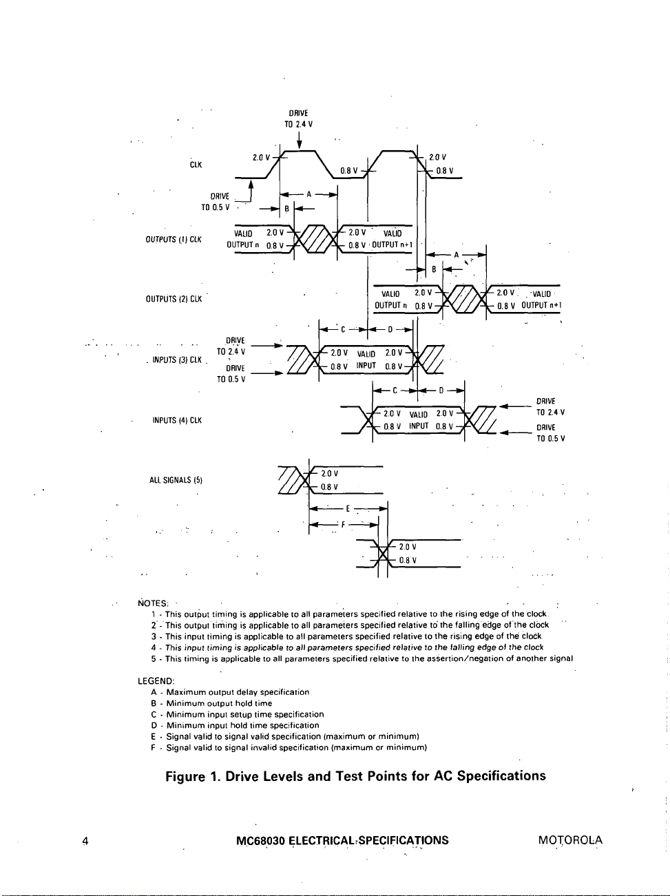
AC ELECTRICAL SPECIFICATIONS DEFINITIONS •
The AC specifications presented consist of output delays, input setup and
hold times, and signal skew times. All signals are specified relative to an
appropriate edge of the MC68030 clock input and, possibly, relative to one
or more other signals.
The measurement of the AC specifications is defined by the waveforms in
Figure 1. To test the parameters guaranteed by MQtorola, inputs must be
driven to the voltage levels •specified in~ Figure 1. Outputs of the MC68030
are specifiedwith minimum.and/or maximum limits, as appropriate, and are
measured as shown. Inputs to the MC68030 are specified with minimum and,
as appropriate, maximum setup and hold times, and are measured asshown.
Finally, the measurements for signal-to-signal specifications are also shown.
Note that the testing levels used to verify conformance of the MC68030 to
the AC specifications:does ~ not affect the guaranteed DC operation of the
device as specified in the DC electrical characteristics.
ME)'~OROEA MC68030!ELECTRICAL SPECIFICATIONS 3
Page 6
' " ' CLK
"
" DRIVE
TO 2.4 V
D°TPUTS(2):L~ ' " VAL'O " '~2"0V 2.OV .'VA"0'
I 00TP,T° 0.aV~V_/_/-'I~_~V OUTPOTo+,
..... , ........ To 2:iv "TA--Y- 2.0 v VAL, O 28 v-&V77
;RIVE IN 0T 08V
T00,v t._c4._0_, t
. INPUTS(4) CLK "-~2E08; :NApL~DT :.::~ T02.4V
ALL
SIGNALS
(S)
NOTES:
-
1 - This out[)ut timing is applicable to all parameters specified relative to the rising edge of the clock
2"-This output'timing is applicable to all parameiers specified relative to" the fallingecIge ofthe cl()ck "
3 - This input timing is applicable to all parameters specified relative to the rising edge of the Clock
4 - This
input
5 - This timing is applicable to all parameters specified relative to the assertion/negation of another signal
LEGEND:
A - Maximum output delay specification
B - Minimum output hold time
C - Minimum input setup time specification
D - Minimum input hold time specification
E - Signal valid to signal valid specification (maximum or minimum)
F - Signal valid to signal invalid specification (maximum or minimum)
timing is applicable to all
V
. --~-- 2.0 V
.~- 0.8 V
parameters specified
relative to the
falling
edge of the clock
.
Figure 1. Drive Levels and Test Points for AC Specifications
4 MC68030 ELECTRICAL-SPECIFICATIONS MOTOROLA
Page 7

DC ELECTRICAL SPECIFICATIONS
(Vcc = 5.0 Vdc_+ 5%; G ND = 0 Vdc; 40 MHz-T A = 0 ° to 70°C, 50 M Hz-TA = 0°C to T C = 80°C)
• .. Characteristic
Input High Voltage
Input Low Voltage
Input Leakage Current
GND ~< Vin ~< VCC
Hi-Z (Off-State) Leakage Current
(, 2.4 V/0.5 V
Output High Voltage
A0-A31, AS, BG, D0-D31, DBEN, DS, ECS, R/W, IPEND,
IOH = 400 p,A
Output Low Voltage
IOL =3.2 mA
IOL = 5.3 mA
IOL = 2.0 mA
IOL = 10.7 mA
BERR, BR, BGACK, CEK,,IPL0-1PL2, AVEC lin -2.5 2.5
A0-A31,'A'~, DBEI~, D--'S, D0-D31, FC0-FC2; ITS I - -20 20
A0-A31, FC0-FC2, SIZ0-SIZ1, BG, D0-D31
CBREQ, AS, DS, R/W, RMC, DSEN, IPEND
,CDIS, DSACKO, DSACK1
OCS, RMC, SIZ0-SIZ1, FC0-FC2,
CBREQ, CLOUT, STATUS, REFILL
HALT, RESET - 20 20
R/W,
RMC, SIZ0-SIZ1
m
STATUS, REFILL, CLOUT, ECS, OCS
Power Dissipation (TA=0°C) " PD , --
Capacitance (see Note) Cin --
Vin=0 V, TA= 25°C, f=l MHz
Load Capacitance ECS, OCS C L --
CLOUT, STATUS, REFILL
: All Other
NOTE: Capacitance is periodically sampled rather than 100% tested.
Symbol Min Max
ViH 2.0 VCC
VIL' GND 0.8
VOH 2.4
VOL
RESET
-0.5
m
m
0.5
0.5
0.5
0.5
2.6
2O
5O
70
130
Unit
V'
"V
~A
#A
V
V
W
pF
pF
AC ELECTRICAL SPECIFICATIONS -- CLOCK INPUT (see
Num. Characteristic
Frequency of Operation
1 Cycle Time Clock
2, 3 Clock Pulse Widtll Measured
from 1.5 V to 1.5 V
4, 5 Clock Rise and Fall Times
20 MHz 25 MHz
Min Max Min Max Min Max Min Max
12.5" 20 12.5 25 20 33.33 25 40
50 80 40 80 30 50 25 40
23 57 19 61 14 36 11.5 29
-- 5 -- 4 -- 3. -- 2
33.33 MHz 40
Figure 2)
MHz
50 MHz*
Min Max
Unit
25 50 MHz
20 40 ns
9.5 30.5 ns
-- 2
ns
*Tcase = 80°C Maximum . .
MoTOR01"A MC68030~EI~ECTRICAI • SPECIFICATIONS 5
Page 8

AC ELECTRICAL SPECIFICATIONS -- READ AND WRITE CYCLES•
(Vcc.= 5.0 Vdc -+5%; GND=0 Vdc; 40 MHz-TA =0 ° to 70°C, 50 MHz-TA =0°.C to TC =80°C)
(see..Figures.3-8)
Num."
6 C!ock'Hig h to Function Code,
6A Clock,High to EC~, OCS ' , 0 15 0 i5 0 12 0 10 0 10 ns
• Asserted I
6B ' Functioni~ode,'Size, RMC,' 4 -- 3 -- 3 -- 'I 3 -- 3 -- ns
7 Clock High to Function Code, O 50 O " 40 O 30 0 25 0 20 ns
.8 Clock High to Fu'nction Code, O -- 0 -- O -- 0 -- 0 -- . ns
9 Clock Low to AS, D'S Asserted,
9A 1 AS toDS Assertion Skew (Read)
9B! 4 AT Asserted to D~ Asserted
10 ECS Width Asserted
"10A OCS Width Asserted
1087 ECS, OCS Width Negated
11 Function Code, Size, RMC,
12 Clock Low to AS, DS, CeREQ' 'O 20 O 18 ' O 10 "O .... 10" O 10' " ns
12A Clock Low to ECS/OCS Negated ..... 0 20
13, AS, DS Negated to Function 1O -- 7 -- 5 :-- 3 -- ~ 3 -- ns
14 AS (and DS Read) Width 85 -- 70 -- 45, --' 30 -- 25 -- ns
' Asserted (Asynchronou's .....
~4A 11 D~ Width Asse'rted (Write) " '
14B " AS (and'DS, Read) Width'
.. Asserted (Synchronous
,15' AS, DSWidth Negated ' " 38 -- 30 -- 23 -- 18 ~ .13 -- .ns
_ .15A 8 ~ Negaied to AT Assertecl .. 30 -- 25 -- 18. -- 16 . . :1~'" -- ns
16 Clock High to AS, DS, R/W, -- 50 40 30 -- 25 I -- 20 ns
Characteristic
Size, RMC, IPEND,
CLOUT, Address Valid
IPEND, CLOUT Address
Valid to Negating Edge of ECS
Size, RMC, CLOUT,
Address Data High
Impedance
Size, RMC, IPEND,
CLOUT, Address Invaiid
CBREQ Valid
(Wri.te)
CLOUT, Address Valid to
Asserting Edge of AS
Asserted (arid DS Asserted,
Read)
Negated
Code, Size, RMC, CLOUT,
Address Invalid .............
Cycle)
Cycle)
DBEN, CBREQ High Impedance
20MHz 25MHz
Min Max Min Max Min Max Min Max Min Max • -
I, 0 25 0 20 0 14 O 14 0 14 ns
3 20 3 18 2 10 2 10 2 10 .ns
-10
10"
-10
32 -- 27 -- 22 -- 16 -- 14 --. ns
15 -- 10 -- 8 -- 5 " -- 4 -- ns
15 -- 10 -- 8 " -- 5 -- 4 -- ns
10 -- 5 -- 5 -- 5 -- 4 -- ns
IO
-- 7 -- 5. -- 5" -- 3 --
O 18 0 15 0 12 ' 0 11 ns'
38 " ~ 30 -- 23" -- 18 m - 13 7 ns
35 -- 30 -- 23 '-- "18 -- 13 -- ns
.33.33MHz
10
-8 8 :6 6 -6 6
40MHz 50MHz*
I
Unit
ns
ns
6 MC68030 ELECTRICAL!SPECIF.ICATIONS MOTOROLA
Page 9

AC ELECTRICAL SPECIFICATIONS
Num.
Characteristic
17' A'--S, D~ Negated to R/W Invalid
18 Clock High to R/~ High
20 Clock High to R/W Low
21 R/W'High to AT 'Asserted
22 R/W Low to D'--S ,~sserted (Write)
23 Clock High to Data-Out Valid
24 Data-Out Valid to Negating
Edge.of AS ..
2511 AS, DS Negated to Data-Out
Invalid
25A 9'11 D-S Negated to DBEN Negated
20MHz 25MHz 33.33MHz 40MHz 50MHz*
Min ,Max Min Max Min Max Min Max Min Max
1Q --- .7" --~ 5 -- 3 -- 3 -- ns
O 25 0 20 0 15 O 14 0 14 ns
0 25 0 20 O 15 0 !4 O 14 ns
10 -- 7 5 -- 5 -- 3 -- ns
60 -- 47 -- 35 -- 24 .-- 23 -- ns
-- 25 -- 20 -- 14 -- 14 -- 14 ns
8 -- 5 -- 3 -- 3 -- 3' -- ns
10 -- 7 -- 5 -- 3 -- . 3 -- ns
10 -- 7 -- 5 -- 3 -- 3 -- ns
(Continued)
" {'
(Write)
2611 Data-Out Valid to Asse~ting Edge 10 -- 7 -- 5 -- 3 -- 3 -- ns
of DS Asserted (Write)
27 Data-In Valid to Clock Low
4 -- 2 -- 1 -- 1 -- 1 -- ns
(Setup)
27A Late BERR/HALT Asserted to
Clock Low (Setup)
2812 AS, DSNegated to DSACKx,
BERR, HALT, AVE C
10 -- 5 -- 3 -- 3 -- 3 -- ns
O 50 0 40 0 30 0 20 0 15 ns
Negated (Asynchronous Hold)
;)8A17 Clock Low to DSACKx, BERR,
HALT, AVEC Negated
12 85 8 70 6 50 6 40 6 35 ns
(Synchronous Hold)
2912 AS, DS Negated, to Data-In
Invalid '(Asynchronous Hold)
29A 12 AS, DS Negated to Data-In
High Impedance
:3012 Clock Low to Da'ta-ln Invalid
(Synchronous Hold)
30A 12 Clock.Low to.Data-In High.
Impedance (Read followed
by Write)
31 ~ . D~ACKx Asserted to Data-In .
Valid (Asynchronous Data.Setup)
31A 3 DSACKx Asserted to DSACKx
. Valid (Skew)
• :32 RESET input Transition Time "
33 CiockLow to B-G Asserted
34 Clock Low to ~ Negated
• .35 BR Assertedto BG Asserted
0 -- 0 -- 0 -- 0 -- 0 -- ns
-- 50 -- 40 -- 30 -- 25 --
20 ns
12 -- 8 -- 6 -- 6 -- 6 -- ns
-- 75 -- 60 -- '45. -- 30' -- 25 ns
-- 43 -- 28 -- 20 -- 14 -- 13 ns
-- 10 -- 7 -- 5 -- 3 -- 3 ns
-- 1,5 .~ 1.5 -- .1.5, ~ .1.5 -- 1.5 Clks
0 25 0 20 0 15 0. , 14 "0 14 ns
0 25 O 20 0 15 0 14 0 14 ns
1,5 3,5 1.5 3.5 1.5 3.5 1,5 3.5 1.5 3.5 Clks
(RMC Not Asserted)
Unit
MOTOROLA MC68030 Er ECTRIGAL;SPECIEICATIONS 7
Page 10

AC ELECTRICAL SPECIFICATIONS
'" 20 MH~' 25 MHz 33~33 MHz 40 MHz 50 MHz*
NUm. " Characteristic
.~ 'Min Max" Min Max Min Max Min Max Min Max
(Continued)
37 BGACK Asserted to BG.Negated 1.5 3.5 1,5 3.5 1.5 3,5 1,5 3.5 1.5 3.5 Clks
37A 6 ,. BG-ACK Asserted to ~ Negated: .0. 1.5 0, 115 0 1.5 0 1.5 0 1.5- Clks
39. BG Width" Negated 75 -- 60 -- 45 -- 30 -- 30 -- ns
39A B'G Width' Asserted 75
@.o J Clock H!gh to DBEN Asserted O 25 0 20 0 18 0 16 0 14 ns
• ! (Read)
--
60
--
45
--
30
--
:30
--
41 C!ock Lowto DBE N Negated O " 25 0 20 0 18 0 16 0 14 ns
(Read)
42 Clock Low to DBEN Asserted 0 25 0 20 0 18 0 16 0 14 ns
(Write)
43 ' Clock High to DBEN Negated O 25 0 20 0 18 0 16 0 14 ns
(Write)
44 R#~ Low to DB~N Asserted 10 -- 7 -- 5 -- 5 -- 5 -- ns
(Write)
455 DB-EN Width Asserted 50 -- 40' -- 30 -- 22 -- 20 -- ns
.... ,~synchronous Read lOg -- 80 -- 60 -- ' 45 --' 40 --
Asynchronous Write
45A 9 DBEN Width Asserted 10 -- 5 --. 5 -- 5 5 -- ns
Synchronous Read 50
Synchronous Write
--
40
--
30
--
22
--
20
46 R/FN Width Asserted 125 -- 100 -- 75 -- 5'0 -- 40 -- ns
".i . (Asynchron0usWrite or'Rea d ) ., .
'46A ' R/W Width'Asserted (Synchronous 75 ' 60
"478 " ~,synchronous Input Hold Time
• 484 DSACKx Asserted to BERR,,
Write or Read)
47A'"
Asynchronous Input Setup Time
to Clock Low
from Clock Low
4 -- 2 -- 2 -- 2 -- 2 -- ns
12 --: 8 --: 6 -- 6 -- 6 -- ns
-- 20 -- 25 -- 18 --. .14 -- 13 ns
--
45
--
30 '
--
25
--
HALT Asserted
53." Data-Out ~'iold from Clock High
55 RAN Asserted to
Data
Bus
3 -- 3 -- 2 -- 2 -- 2 -- ns
25 -- 20 -- 15 -- 11 -- 11 -- ns
Impedance Chan~je
56 RESE=r Pulse Width
512 -- 512' -- 512 -- 512 -- 512 -- Clks
(Reset In'struction)
57 BERR
58 l° BGACK Negated to Bus Driven
59 l° B'-G Negated to Bus Driven
Negated to
Negated (Rerun)
HALT
0 -- 0 -- 0 -- 0 -- O -- ns
I -- .I --
I -- I -- 1 -- 1 -- I --
1
-- .I -- I -- Clks
Unit
ns
ns
Clks
8' MC68030 EI'ECTRICALSPECIEICATIONS MOTOROLA.
Page 11

AC ELECTRICAL SPECIFICATIONS (Concluded)
Num. Characteristic
6013 Synchronous Input Valid to 4 -- 2 --
6113 !Clock High to Synchronous 12 -- 8 --
NOTES:
*Tcase = 80°C Maximum
1. This number can be reduced to 5 ns if strobes have equal loads.
2. If the asynchronous setup time (#47A) requirements are satisfied, the DSACKx low to data setup time (#31) and
3. This parameter specifies the maximum allowable skew between DSACK0 to DSACK1 asserted or DSACK1 to DSACK0
4. This specification applies to the first (DSACK0 or DSACK1) DSACKx signal asserted. In the absence of DSACKx, BERR
5. DBEN may stay asserted on consecutive write cycles•
6. The minimum values must be met to guarantee proper operation. If this maximum value is exceeded, B'-G may be
7. This specification indicates the minimum high time for ECS and OCS in the event of an internal cache hit followed
8. This__specification guarantees ~)peration with the MC68881/MC68882, which specifies a minimum time for ~ negated
9. This specification allows a system designer to guarantee
10. These specifi(;ations allow system designers to guarantee that an alternate bus master has stopped driving the bus
.11. DS will not be asserted for synchronous write cycles with no wait states~
12. These hold times are specified with respect to strobes (asynchronous) and with respect to the clock (synchronous).
13. Synch?or~ous__ inputs must meet specifications #60 and #61 with stabJe logic levels for
14. This specification allows system des~qners'._.tto qualify the~ signal of an MC68881/MC68882 with AT (allowing 7 ns
Clock High (Setup Time)
Input Invalid (Hold Time)
62 Clock Low to STATUS, 0 25 O 20
REFILL Asserted
63 Clock Low to STATUS, 0 25 0 20
REFILL Negated
DSACKx low to BERR low setup time (#48) can be ignored. The
time (#27) for the following clock Cycle, and BERR must only satisfy the late BERR low to clock low setup time (#27A)
for the following clock cycle.
asserted specification #47A must be met by DSACK0 or DSACK1.
is an asynchronous input using the asynchronous input setup time (#47A).
reasserted.
immediately by another cache hit, a cache miss, or an operand cycle.
• to,AS asserted (specification #13A in the
• interpretation of specifications #9A and #15 would indicate that the MC68030 does not meet the MC68881/MC68882
requirements.
output enable signals generated with DBEN. The timing on DBEN precludes its use for synchronous READ cycles with
no wait states.
when the MC68030 regains control of the bus after an arbitration sequence.
The designer is free to use either time.
while AS is asserted. These values are specified relative to the high level of the rising clock edge The values originally
published were specified relative to the low level of the rising clock edge.
for a gate delay) and still meet the CS to DS setup time requirement (spec 8B) of the MC68881/MC68882.
20 MHz 25 MHz
Min Max Min Max
MC68881/MC68882 User's Manual).
data
33.33 MHz 40 MHz 50 MHz*
Min Max Min Max Min Max
2 -- 2 -- 2 -- ns
6 -- 6 -- 6 -- ns
O 15 0 15 0 15 ns
0 15 O 15 0 15 ns
data
must only satisfy the data-in clock low setup
Without this specification, incorrect
hold times on the output side of data buffers that have
all
rising edges of the clock
Unit
MOTOROLA MC68030 ELECTR CAL.~SPEC F, CATIONS 9
Page 12

Figure 2. Clock Input Timing Diagram
. . ... ,,. .
.-@
10 MC68030 ELECTRICAESPECIEICATIONS MOTOROLA
Page 13

CLK
$1 $2 $3
__2 ~"-2- .__ .
$4 $5
AO-A31, FCO.FC2
SIZ0-SIZI
RMC
oc-g -- ~
R/W
DSACKO
OSACKI
8ERR
HALT
~-.~ @
~_
®
(~- ~
(5>. ®
(~.
m
m
®
®
®
---i
.- ],.
.@
ASYNCHRONOUS
MOTOROLA MC68030 ELEC'TRICAE~SPECIFICATIONS 11
ALL
INPUTS
CIIN
Figure 3. Asynchronous Read Cycle Timing Diagram
¥
%
%
.
' ~'~)
Page 14

A0-A31, FC0-FC2 /
SIZ0-SIZ1
RMC- .
~_ --~ ®
SO SI $2 $3 . $4
$5 SO
'0-'~ .Z,
@
.
- _/ ®
00-031
---tP
-.4 ~
--.<~
F.igure:4: Asyncliro'nous Write .Cycle Timing.Diagram
12 MC68030"EI~ECTRIC'AL SPE~:IFICP, TiONS MOTOI~OI"A"
Page 15

SO $1 $2
AO-A3!. FC0-FC2 ,,--__%
SIZO-SIZ1 --J
.RMC
[c-~ ---~,
DBEN
CLOUT
CBREO
i,.--
-
.®
...@_
i i
S3 SO Sl S2
• --lID ,).4.-4 8 I-."
,,.
-@
t" ,
OSACK0/0SACKI J
STERM
CIIN
CBACK
00-031
"1
Figure 5. Synchronous ReadCycle Timing Diagra m
MOTOROLA MC68030 ELECTRICAL SPECIEICATIONS 13
• • , . . ........
Page 16

CLK
A0-A31. FC0-FC2
SIZ0-SlZ~i
RMC
ECS
m
OCS
R/W
00.031
SO SI $2
• A~."
S3 SO
Sl S2
OSACK0/DSACKI
.___/
.... 141
HAL'--"T .. z ~ r
Figure 6. Synchronous Write Cycle Timing Diagram
14 MC68030"EI'ECTRICAL SPECIF.ICATIONS MOTORO#A':
Page 17

SO $1 $2 $3 $4 $5
CLK
A0-A31 ~ '
00-031
FC0-FC2
SIZ0 -SIZ I
EC7 ~___~
R/W
DBEN
0SACK0
0SACKI
<
\
\
\
\ '
®
4:
--t_
86ACK
i
Figure 7. Bus Arbitration Timing Diagram
MOTOROLA MC68030 ELECTRICAL SPECIEICATIONS 1:5
®
/
I
i
Page 18

CLK ~
IPENO
MMU01S
C01S
STATUS
REFILL
}
Figure 8. Other Signal Timings
16 MC68030 ELECTRICAl' SPECIFICATIONS MOTOROLA
Page 19

Literature Distribution Centers:
USA: Motorola Literature Distribution; P.O. Box 20912; Phoenix, Arizona 85036.
EUROPE: Motorola Ltd.; European LiteratUre Center; 88 Tanners Drive, Blakelands, Milton Keynes, MK14 5BP, England.
ASIA PACIFIC: Motorola Semiconductors H.K. Ltd.; P.O. Box 80300; Cheung Sha Wan Post Office; KowIoon Hong Kong.
JAPAN: Nippon Motorola Ltd.; 3-20-1 Minamiazabu, Minato-ku, Tokyo 106 Japan.
"
B MOTOROLA
=
., , .
MC68030EC/D
 Loading...