

Page 1
——
-——— -—
查询6800供应商
8-BIT MICROPROCESSING UNIT (MPU)
The MC6800 is a monolithic 8-bit microprocessor forming the central
control function for Motorola’s M68~ family. Compatible with TTL, the
MC6B~, as with all M6800 system parts, requires only one + 5.O-volt
power supply, and no external TTL devices for bus interface.
The MC6800 is capable of addressing 64K bytes of memory with its
16-bit address lines. The 8-bit data bus is bidirectional as well as threestate, making direct memory addressing and multiprocessing applications realizable.
● 8-Bit Parallel Processing
● Bidirectional Data Bus
. 16-Bit Address Bus – WK Bytes of Addressing
● 72 Instructions – Variable Length
. Seven Addressing Modes – Direct, Relative, Immediate, Indexed,
Extended, Implied and Accumulator
● Variable Length Stack
. Vectored Restart
. Maskable Interrupt Vector
. Separate Non-Maskable Interrupt – Internal Registers Saved i#’’::$$
Stack
. Six Internal Registers – Two Accumulators, Index Regist~#?Y’:Y’
Program Counter, Stack Pointer and Condition Code Re~@te~
● Direct Memory Addressing (DMA) and Multiple P~@$esso’r
Capability
● Simplified Clocking Characteristics
. Clock Rates as High as 2.0 MHz
● Simple Bus Interface Without TTL ,$~~~~i$~’
● Halt and Single Instruction Executlo*k$~~$bility
~~$$~
....,
,.,.$,.>.‘i,\,.*>
& ‘~~$
..,.
,{,
,:&f*,>~<~’
,>$
$$:$
~:
.~~....
~+~,
\*:,.:~’‘
,*.. .+
\,\<\!;..
.,\.J.*.+,t~
..
,,,~~&Y@’DERING
w<, .-1. $,)
INFORMATION
PackageType‘$:,~~equency (MHz)
ceramic+,,:,~f~ “
L s~~i~ ~ “
@y*+(k:::
Ti. .... ,
~rdio
.—
!–!–
s suffix
1.0
1.0
2.0
1.0 O“c to 70°c
1.0 –40°C to 85°C
*:;.>
,.*. .\
‘;:$*Y*:,F
.it~
Temperature Order Number
Ooc to 70°c
–40°C to 85°C MC~~CL
Ooc
to 70°c
.:;.!,.,, ...+
,1’.-‘ -->,,:+~..,
*V\>>>.,,**.
‘~:?iii*
...*”,+<
,,:+,..,
‘.~;:),t.{t,.
,~>
,“,.,
I
1.5 O“c to 70°c
1.5 –40°C to 85°C
O“c to 70°c
–40°C to 85°C
to 70°c MC68AOOP
to 85°C
to 70°c MC68BOOP
Plastic
P Suffix
2.0
1.0 O“c to 70°c
1.0
1.5 O“c
1.5 – 40°C
2.0 Ooc
*: ,.. ‘is
.,>s,-.
MC6800L
MC68BOOL
MC68WS
MC@WCS
Mc68Ams
Mc68Amcs
MC68BOOS
MC6800P
MC6800C P
MC68AOOCP
,,2:+.(~
‘~”‘%1*F.
, ~,,)i~. ,{).
.Y,:>,+,-,,,..,,,!,.
........
.}.
,,*!.
“)!.IC,[
~..!’.
,>:
‘.*$
MCWOO
uu. -
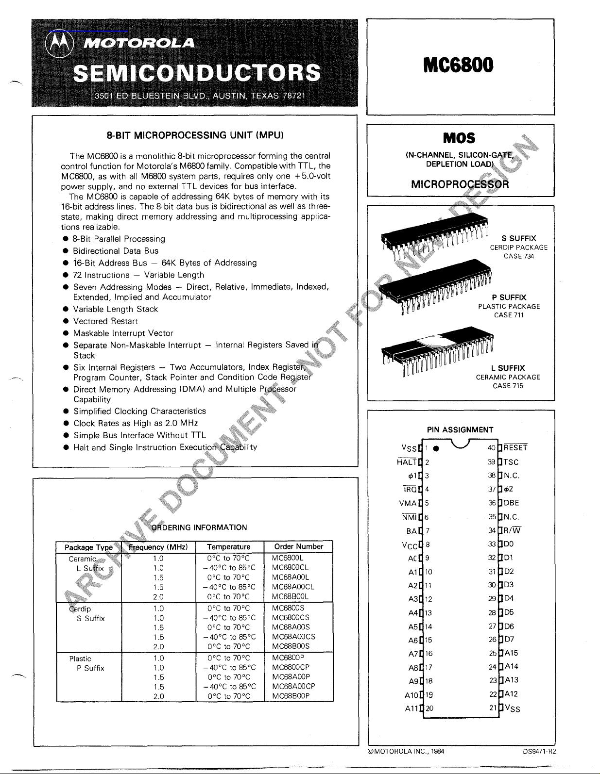
PIN ASSIGNMENT
Vss[ 10
HALT[ 2
@l [ 3
4
KQ [
VMA [ 5
6
m[
BA [ 7
Vccc 8
AC[ 9 32 ]Dl
Al [ 10 31 ] D2
A2 [ 11
A3[ 12
A4[ 13 28 ] D5
A5 [ 14
A6 [ 15
A7 [ 16 25 ]A15
A8 [ 17
A9 [ 16
A1O c
19
Al 1q 20
CERAMIC PACKAGE
~
SUFFIX
CASE 715
JRESET
39
]TSC
38 ]N. C.
37 342
36 ]DBE
35 ]N, C.
34 ]Rl~
33 ] DO
30 ] D3
29 ] D4
27 ] D6
26 ] D7
24 ]A14
23 JA13
22 ]A12
21 Jvss
I
i
I
MOTOROLA INC., lW
DS9471-F
Page 2
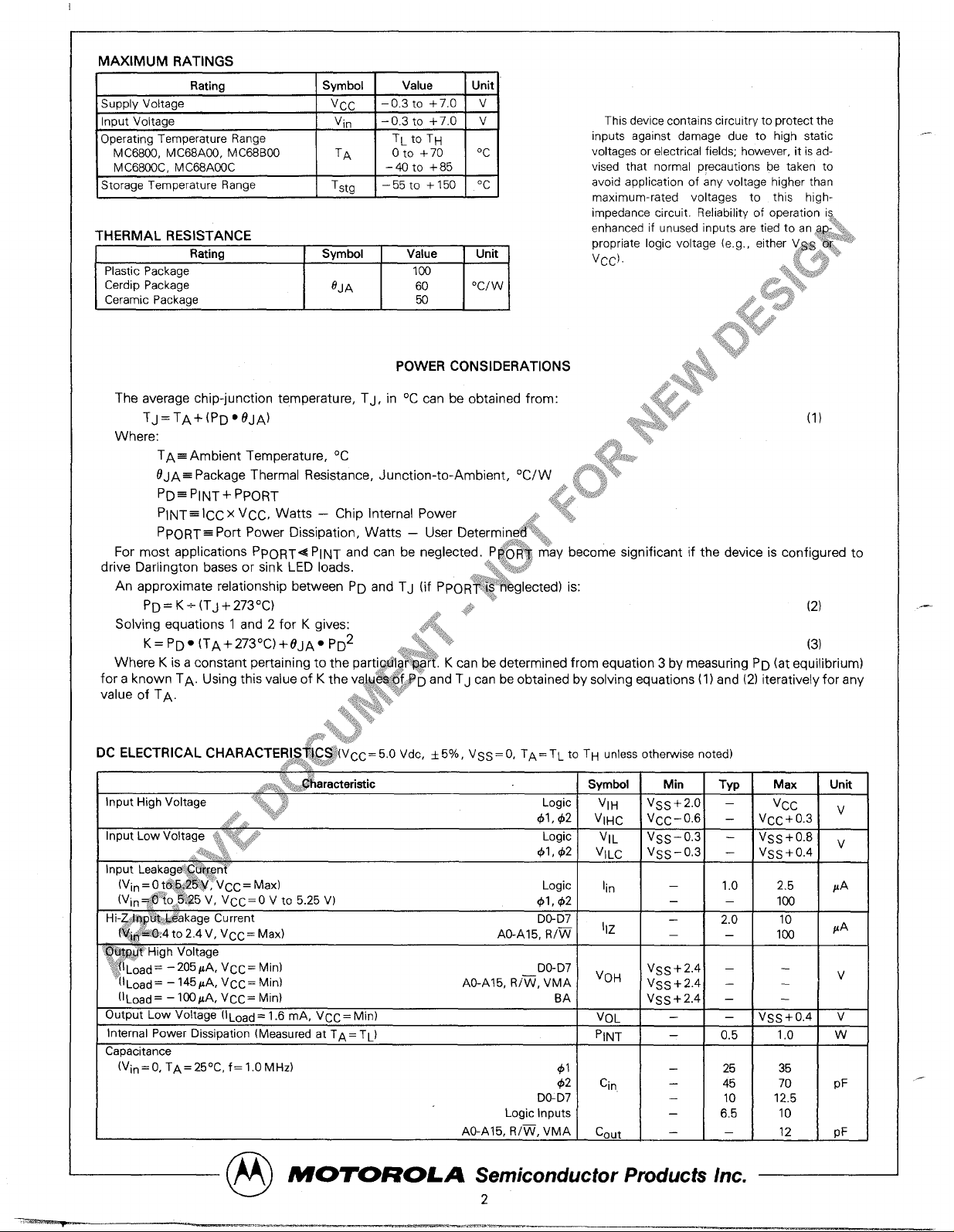
MAXIMUM RATINGS
MC6~C MC68A~C
I I -40to +85 I I
Storage Temperature Range
I Tsta l-55to +150 I “C I
THERMAL RESISTANCE
Rating
Symbol Value Unit
Plastic Package Im
Cerdip Package
eJ A
60
“Clw
Ceramic Packaqe m
POWER CONSIDERATIONS
The average chip-junction temperature, TJ, in ‘C can be obtained from:
TJ=TA+(PDo OJA)
Where:
TA = Ambient Temperature, ‘C
This device contains circuitry to protect the
inputs against damage due to high static
voltages or electrical fields; however, it is advised that normal precautions be taken to
avoid application of any voltage higher than
maximum-rated voltages to this highimpedance circuit. Reliability of operation is
(1)
OJA= Package Thermal Resistance, Junction-to-Ambient, “C/W ;F’s~;
,.,\\wy\~.::$,i~
PD=PINT+PpORT
.,$ ‘f:?ki,,, ,,$3
~..,..,..
::i~.’.~i.:.,.
PINT= ICC x Vcc, Watts – Chip Internal Power
.<,,..,,
1*+:
,..,
.,+*
PpORT = Port Power Dissipation, Watts – User Determin@:$,,,
. ,.,. .
..,.
For most applications PPORT< PINT and can be neglected. P$o~~ may become significant if the device is configured to
drive Darlington bases or sink LED loads.
%i*\:,+,:,,,**F
..,,,.,,\+,*
An approximate relationship between PD and TJ (if PpO~~$YWbglected) is:
,.>,,,.
PD= K- (TJ+2730C)
~,:*
(2)
.,J:>
Solving equations 1 and 2 for K gives:
,J,t::i,}
.,(*;{:\
K= PD. (TA+2730C)+0JA* PD2 .. ‘}~. $
(3)
,’,:::/:’\,.*:..*>.\\
Where K is a constant pertaining to the parti~$~$~~~it. K can be determined from equation 3 by measuring PD (at equilibrium)
for a known TA. Using this value of K the va~~~~:Qft,@Dand TJ can be obtained by solving equations(1) and (2) iteratively for any
value of TA,
\\*‘:*,.
.,,
,>f:?>,{,,,>i,,t
~“,’.,,\<..
.~\ ‘~$,\.,!.{w
‘-.<~:,.~~y>
V’i,
.\\
,::,2.CF i?~jt:,?..
.},.
DC ELECTRICAL CHARACTERl~%~C~(Vcc= 5,0 Vdc, +5%, Vss = O, TA= TL to TH unless otherwise noted)
,..:$:,?,$,,,..,,.,>
“ ~~@aracteriatic
\t$.<,%,\..&i,t.
Input High Voltage
“i’;,,L,,‘$,
Logic
“a?+$,}.,,’~
,;>?
~.,t...t,
41,42
Input Low Voltage ~w”$&~$,$#
Logic
.,. , ‘<$
.,~’tat;.{,,,\.:,,
~1 ,42
*,,.;’.
Input Leakag@:$~&f$n~
(Vin =Ot&@&~~, Vcc= Max)
Logic
(Vin
~&!0,~~@5 V, Vcc=o V to 5.25 V)
Hi-~@bkti@akage Current
@l, #2
D&D7
f~#’@&.4 to 2.4 V, Vcc = Max)
AO-A15, Rlw
~w~? High Voltage
‘$$lLoad= - 205tiA, Vcc= MinJ
DO-D7
“(lLoad= – 1454A, VCC= Min)
A&A15, R/~, VMA
(lLoad= – 100KA, VCC= Min)
BA
Output Low Voltage (lLoad = 1.6 mA, VCC = Min)
Internal Power Dissipation (Measured at TA = TL)
Capacitance
(Vin=O, TA=250C, f=l.O MHz)
~1
42
DGD7
Logic Inputs
AO-A15, Rl~, VMA
—
Svmkl
VOH
VOL
PINT
Cin
Cout
VSS–0,3 –
VSS+O.8 v
VSS–0,3 –
VSS+O.4
—
1,0
2.5
PA
,
[
1
I
VSS+2.4 – –
VSS+2.4 – –
v
VSS+2.41 – I – I
I
—
!
—
Ivss+o
w
,4 v
—
I 0.5 ]
1,0 w
I I I I
—
25 35
—
45
70 pF
—
10 12.5
—
6.5
10
— —
12 pF
(M)
MOTOROLA Semjconducfor Products Inc.
.-
2
Page 3
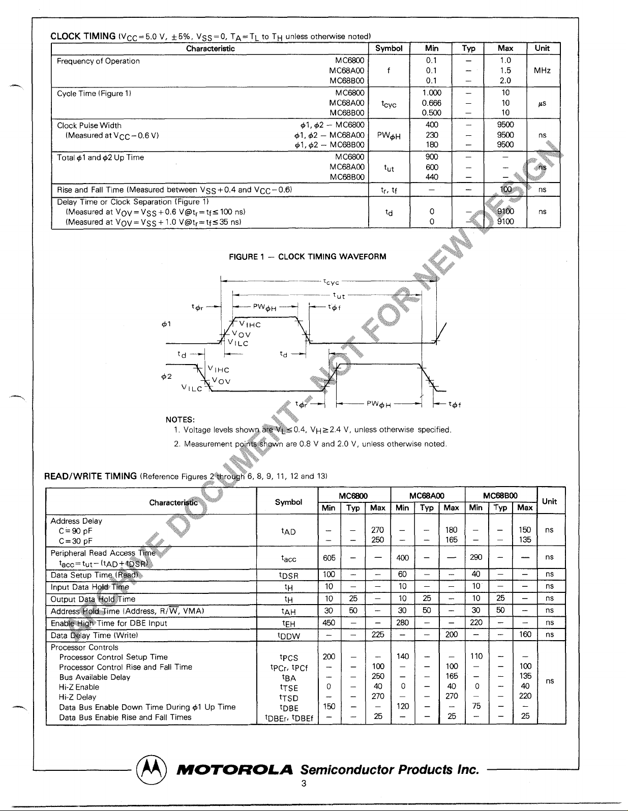
CLOCK TIMING (Vcc= 5,0 V, *5%, VSS=O, TA=TL to TH unless otherwise noted)
Characteristic
Frequency of Operation
Cycle Time (Figure 1)
Clock Pulse Width @l, @2– MCmN
(Measured at VCC– 0.6 V)
Total 01 and 42 Up Time
Rise and Fall Time (Measured between VSS +0.4 and VCC– O.6)
Delay Time or Clock Separation (Figure 1)
(Measured at VOV=VSS+O.6 V@tr=tf=l~ ns)
(Measured at VOV= VSS + 1.0 V@tr=tf S35 ns}
@l, @2– MC6BAO0 pW~H
@l, @2 – MC68BO0
MC~
MC68AO0 f
MCWBW
MCm 1.000 –
MC@AW
MC~BW
MCH
MC~A~
MC6BBW
Symbol Min Typ
0.1 –
0.1 –
0.1 –
tcyc
t“t
tr, tf
td
O.m
O.m – 10
w – 9m
Za –
180 –
90 –
600 –
w –
~
— —
o
o
—
–$; y< “$,~
—.$:~,
?\:i..
Max Unit
9m
9W
,,fj:$’,i~ ,’;?,..~’
%$*t&
,>+1,:
,,
$\*.’,
1.0
1.5 MHz
2.0
10
10 ps
ns
—
–
– ‘$$:fi+s:~
1
, ,,,,
.!>.,:..,.,.:~:~,
Y “~:..
d*“:*’:*L
ns
,*!.
‘*{,1,
td+ +
vl~c*
,, ...>.,,,.
.~t~
4:.
*T, ,+1
,
,~.;.,+-.~’--:$,
..,,.
~,t~,,,:y
- .$~~+’<.~a..~+,k~
~\+,\ -i
*,. :
‘:.$.....
,,,,
tDBEr, tDBEf
Character@i&$iF, ~~’
Address DelaV
C=90pF
C=30 pF
Peripheral Read Access ~fi&~f:
tacc = tut – (tAD +~~~$~.
Data Setup Tim$,:( ~~~?:
Input Data H@me ‘
Output D~@ ‘~l,#Time
Addressf&,&,Jime (Address, R/~, VMA)
Ena~~i~@Time for DBE Input
Data ~lav Time (Write)
Processor Controls
Processor Control Setup Time
Processor Control Rise and Fall Time
8US Available DelaV tBA
Hi-Z Enable
Hi-Z DelaV
Data Bus Enable Down Time During @l Up Time
Data Bus Enable Rise and Fall Times
**3::,:>
,,..,.. >
‘d+ b,’’”
..,,
,.
,, <
Symbol
tA D –
tacc
tDSR
tH 10
tH 10
tA H 30
tEH 450
tDDW
tpcs
tpcr, tpcf
tTSE o – 40 0
tTSD
tDBE
MC~
Min
Typ Max Min
270 –
–
— —
605
lm
– – 225 –
2m
– – Im –
– – 29 –
– –
Iw
– – 25
2W –
– — m
– – 60
– – 10
25 – 10
50 – 30
– –
– – 140
270 –
– –
MC8BAO0
Typ Max Min
–
–
– — 2W
– – 40
– – 10
25 – 10
a – m
280
– –
– 2W –
– –
– 100 –
–
– 40 0
–
120
– –
–
– 25
1BO –
165 –
165 –
270 –
MC6BBO0
220
110
75
–
Typ Max
– 150 ns
135
–
– — ns
– – ns
– – ns
25 – ns
50 – ns
– – ns
– 160
–
–
– 100
135
–
– m
220
–
– –
–
25
Unit
ns
ns
—
m
M070ROLA Semiconductor Products Inc.
3
Page 4
1
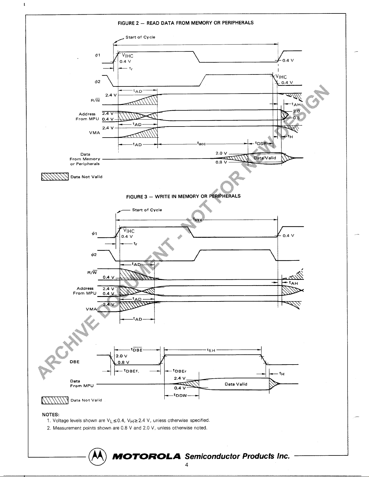
FIGURE 2 – READ DATA FROM MEMORY OR PERIPHERALS
/
Start of Cycle
+
@l
‘VIHC
~
0.4 v
7
0.4 v
Data Not Valid
~ Start of Cvcle
‘):.,
[
Data
2.4 V
From MPU
0.4 v
I
k\\\\\\Y
Data Not Valid
ktDDw+
NOTES:
1. Voltage levels shown are VLSO.4, VH> 2.4 V, unless otherwise specified
2. Measurement points shown are 0.8 V and 2.0 V, unless otherwise noted
@
MOTOROLA Semiconductor Produck Inc.
4
—
Page 5
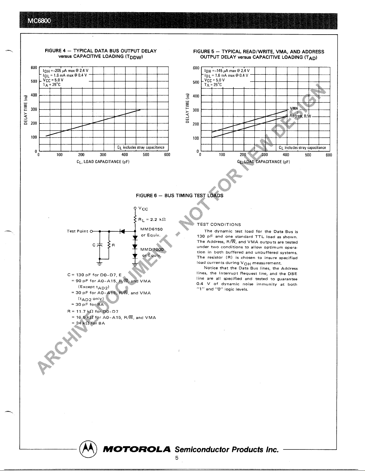
FIGURE 4 – TYPICAL DATA BUS OUTPUT DELAY
versus CAPACITIVE LOADING (TDDw)
600
I OH =-205A max @ 2.4 V
‘lo L=l.6mAmax@0.4V
500 -
Vcc = 5.0v
1A= 25°C
~ 400
=
u
z
F 300
>
/
~
/ ~
: 200
/ ‘
- ~
/
100
/
CL
includes stray capacitance
0’
0 100 200
300
400 500 600
CL,
LOAO CAPACITANCE (pF)
FIGURE 5 – TYPICAL READ/WRITE, VMA, AND ADDRESS
OUTPUT DELAY
versus CAPACITIVE LOADING (TAD)
600
lo H=-145*max@2.4V
‘lo L=l.6mAmax@0.4v
500
-VCC=5.OV
TA = 25°C
-$,:,
z 400
u
z
~ 300
~
u
0 200
100
CL
includes stray capacitance
o
0 100
2og~+~~ ,i$oo
400
500
600
@
MOTOROLA Semiconductor Products Inc.
5
Page 6
I
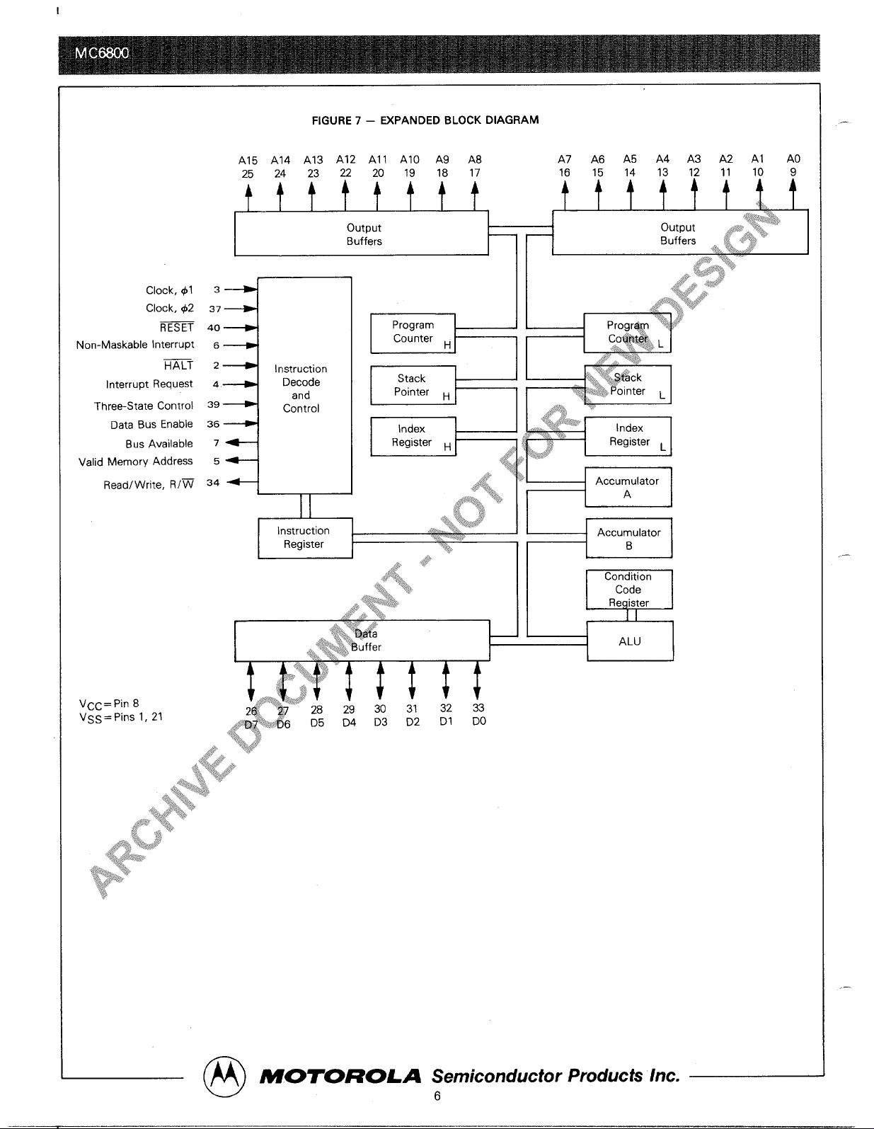
FIGURE 7 – =PANDED BLOCK DIAGRAM
A15 A14 A13 A12 All A1O A9 A8
A7 A6 A5
A4 A3 A2 Al AO
Clock, @l
Clock, @2
RESET
Non-Maskable Interrupt
HALT
Interrupt Request
Three-State Control
Data Bus Enable
Bus Available
Valid Memory Address
Read/Wtite, Rl~
37
40
6
a
2
3
Instruction
4
Decode
and
39
Control
36+
34+
1
Instruction
Register
‘*” !*
..l.t\,,
@
MOTOROLA Semiconductor Products Inc.
6
.—
.—
.—
Page 7
MPU SIGNAL DESCRIPTION
Proper operation of the MPU requires that certain control
and timing signals be provided to accomplish specific functions and that other signal lines be monitored to determine
the state of the processor.
Clocks Phase One and Phase Two (o1, 42) – Two pins
are used for a two-phase non-overlapping clock that runs at
the VCC voltage level.
Figure 1 shows the microprocessor clocks. The high level
is specified at VIHC and the low level is specified at VILC.
The allowable clock frequency is specified by f (frequency).
The minimum @l and @2 high level pulse widths are specified
by PW~H (pulse width high time). To guarantee the required
access time for the peripherals, the clock up time, tut, is
specified. Clock separation, td, is measured at a maximum
voltage of VOV (overlap voltage), This allows for a multitude
of clock variations at the system frequency rate.
Address Bus (AOA15) – Sixteen pins are used for the address bus. The outputs are three-state bus drivers capable of
driving one standard TTL load and 90 pF. When the output is
turned off, it is essentially an open circuit. This permits the
MPU to be used in DMA applications. Putting TSC in its high
state forces the Address bus to go into the three-state mode.
Data Bus (DO-D7) – Eight pins are used for the data bus.
It is bidirectional, transferring data to and from the memory
and peripheral devices. It also has three-state output buffer$
capable of driving one standard TTL load and 130 pF. D,a~$,
Bus is placed in the three-state mode when DBE is Io#t\,t w~$.
,{’.y...:>.:>,,:!:.?..
.+,.‘+:+”‘ ‘$,.?
Data Bus Enable (DBE) – This level sensitive i~[~t~$sthe
three-state control signal for the M PU data ~$~l:~yd will
enable the bus drivers when in the high st~:&$$@j9 Input is
TTL compatible; however in normal op~,atib~~$twould be
driven by the phase two clock. Durin&@n~~,K~ read cycle,
the data bus drivers will be disabled,’~~t~nal ly. When it is
desired that another device contr$PtR~&ata bus, such as in
Direct Memory Access (DMA)j+~k~@~ions, DBE should be
held low.
~t~
.>.:,:,.,,, ,x.
If additional data setup+p[+ho~d~?me is required on an MPU
write, the DB E
down ,~,~~ @n be decreased, as shown in
Figure 3 (DBE#@2\R:~~e~inimum down time for DBE is
tDB E as shown, ~~~.s}~ting D B E with respect to E, data
setup or hold t~,$@# be increased.
\\\$.
;>L:.,.?J~,
Bus Ay~i$~l~.(bA) – The Bus Available signal will nor-
mally ~%~ ~}$’low state; when activated, it will go to the
..,*.’:* Y
high.?ata~:+indicating that the microprocessor has stopped
* “’“’*’l+
and @,@tfhe address bus is available. This will occur if the
HALT~ne is in the low state or the processor is in the WAIT
state as a result of the execution of a WAIT instruction. At
such time, all three-state output drivers will go to their off
state and other outputs to their normally inactive level. The
processor is removed from the WAIT state by the occurrence
of a maskable (mask bit I= O) or nonmaskable interrupt, This
output is capable of driving one standard TTL load and
30 pF. If TSC is in the high state, Bus Available will be low,
Read/Write (R/~) – This TTL compatible output signals
the peripherals and memory devices wether the MPU is in a
@
MOTOROLA
Read (high) or Wrile (low) state, The normal standby state of
this signal is Read (high). Three-State Control going high will
turn Read/Write to the off (high impedance) state. Also,
when the processor is halted, it will be in the off state. This
output is capable of drivina one standard TTL Ioa&?iqnd
90 pF.
~+,r+i~ .:}
RESET – The RESET input is used to rese~&}N~&~rt the
M PU from a power down condition resulti~~,jf~% a power
failure or initial start-up of the processor,+:~@l%~i&el sensitive
input can also be used to reinitialize t,$~~~~~ne
at any time
after start-up.
.)’ k%}?*
:t:;l,\ \
If a high level is detected in th~ Inpw; this will signal the
MPU to begin the reset seqe~$~. During the reset sequence, the contents of th,~?%f$wb locations (FFFE, FFFF)
in memory will be loade@{~~&,Jtie Program Counter to point
to the beginning of..,$~b.:wet routine. During the reset
~.\J~t.~,,~y..
routine, the interrupt ~s~ bit is set and must be cleared
under program c~~ol, before the M PU can be interrupted by
IRQ. While ‘K%Jk’’low
(assuminga minimum of8 clock
cycles have ~Jcc~$r8d) the MPU output signals will be in the
followinqj$&MVMA= low, BA= low, Data Bus= high impeda~~e,>~~~= high (read state), and the Address Bus will
con$&8 the ‘reset address FFFE. Figure 8 illustrates a power
?}4
&“~q@~nce using the RESET control line. After the power
~i.
~,P@ reaches 4.75 V, a minimum of eight clock cycles are
?$:jlj$~qtiired for the processor to stabilize in preparation for
‘~trestarting. During these eight cycles, VMA will be in an in-
.lp~
determinate state so any devices that are enabled by VMA
which could accept a false write during this time (such as
battery-backed RAM) must be disabled until VMA is forced
low after eight cycles. RESET can go high asynchronously
with the system clock any time after the eighth cycle.
RESET timing is shown in Figure 8. The maximum rise and
fall transition times are specified by tpcr and tpcf. If RESET
is high at tpcs (processor control setup time), as shown in
Figure 8, in any given cycle then the restart sequence will
begin on the next cycle as shown. The RESET control line
may also be used to reinitialize the MPU system at any time
during its operation. This is accomplished by pulsing RESET
low for the duration of a minimum of three complete 42
cycles. The RESET pulse can be completely asynchronous
with the MPU system clock and will be recognized during 42
if setup time tpcs is met.
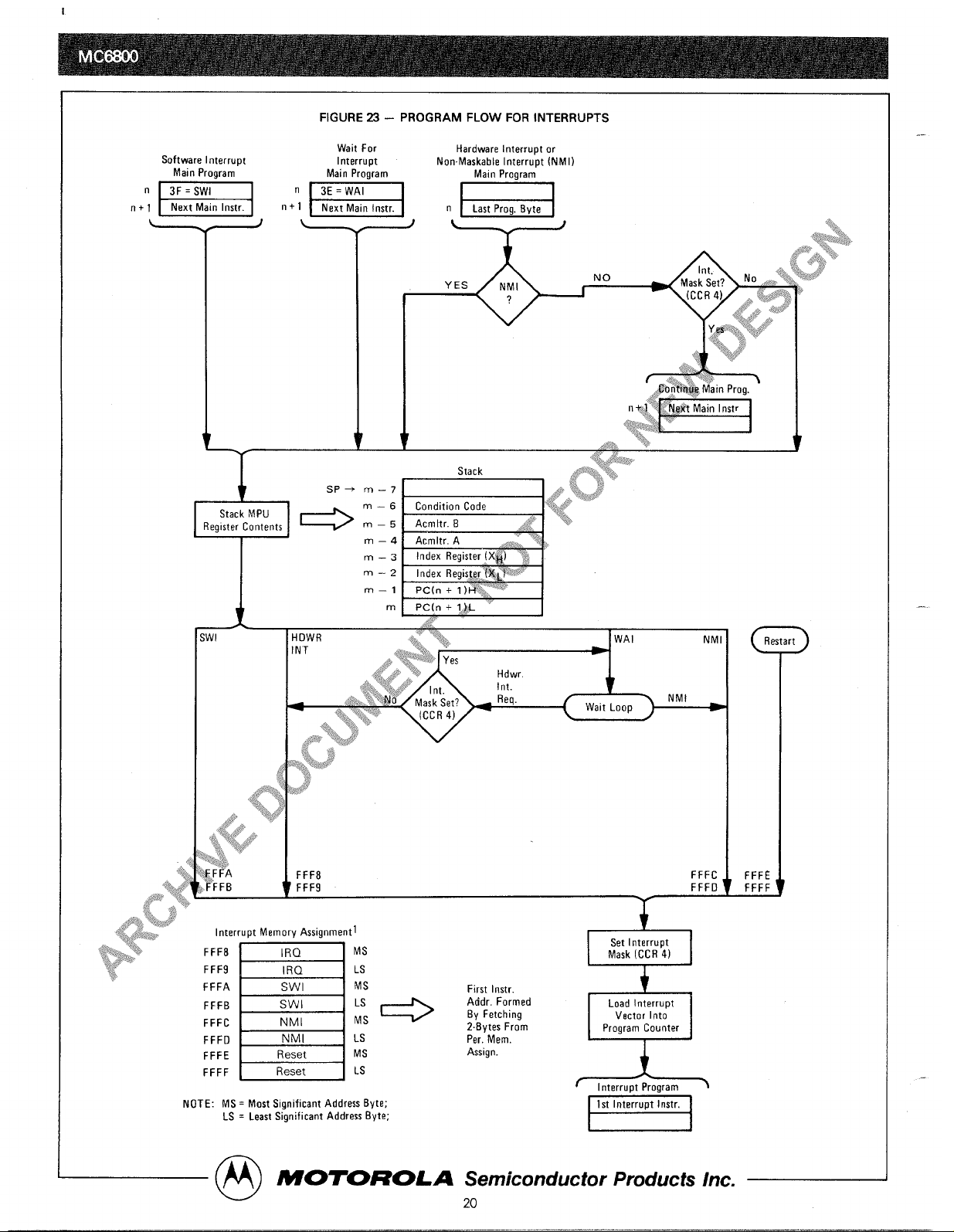
Interrupt Request (~Q) – This level sensitive input re-
quests that an interrupt sequence be generated within the
machine. The processor will wait until it completes the current instruction that is being executed before it recognizes
the request. At that time, if the interrupt mask bit in the Condition Code Register is not set, the machine will begin an interrupt sequence. The Index Register, Program Counter, Accumulators, and Condition Code Register are stored away on
the stack. Next, the MPU will respond to the interrupt request by setting the interrupt mask bit high so that no further
interrupts may occur. At the end of the cycle, a 16-bit address will be loaded that points to a vectoring address which
is located in memory locations FFF8 and FFF9. An address
loaded at these locations causes the MPU to branch to an in-
terrupt routine in memory. Interrupt timing is shown in
Figure 9.
Semiconductor Products Inc.
7
Page 8

Page 9
The HALT line must be in the high state for interrupts to
be serviced. Interrupts will be latched internally while HALT
is low.
The ~ has a high-impedance puilup device internal to
the chip; however, a 3 kQ external resistor to VCC should be
used for wire-OR and optimum control of interrupts.
Non-Maskable Interrupt (NMI) and Wait for Interrupt
(WAI) – The MCWCO is capable of handling two types of interrupts: maskable (~) as described earlier, and nonmaskable (~) which is an edge sensitive input. IRQ is
maskable by the interrupt mask in the condition code register
while ~ is not maskable. The handling of these interrupts
by the M PU is the same except that each has its own vector
address. The behavior of the MPU when interrupted is
shown in Figure 9 which details the MPU response to an interruDt while the MPU is executina the control ~roaram. The
interrupt shown could be either ~Q or ~ and ca~ be asynchronous with respect to +2. The interrupt is shown going
low at time tpcs in cycle #1 which precedes the first cycle of
an instruction (OP code fetch). This instruction is not executed but instead the Program Counter (PC), Index
Register (IX), Accumulators (ACCX), and the Condition
Code Register (CCR) are pushed onto the stack,
The Interrupt Mask bit is set to prevent further interrupts.
The address of the interrupt service routine is then fetched
fram FFFC. FFFD for an NMI interruDt and from FFF8, FFF9
for an ~’interrupt. Upon complet~on of the interrupt service routine, the execution of RTI will pull the PC, IX, ACCX,
and CCR off the stack; the Interrupt Mask bit is restored to
its condition prior to Interrupts (see Figure 10).
Figure 11 is a similar interrupt sequence, except in this
case, a WAIT instruction has been executed in prepara$$~
for the interrupt. This technique speeds up the M&U’”~
response to the interrupt because the stacking of
tbe~~~$.W,
ACCX, and the CCR is already done. While t~~$fM@ iS
waiting for the interrupt, Bus Available wilP&@+{Q?~hindicating the following states of the control lj~~Y~MA is
low,
and the Address Bus, R/~and Data B~~ ~~, ~{ in the high
impedance state. After the interrupt w-$* ISserviced as
previously described.
,.\,
.<
},it?~,,,::
A 3-10 kQ external resistor to V&*’&~&tild be used for wire-
OR and optimum control of igi~r~w~t~.
,*+$
..,,.
“$,’
..
MEMORY MAP.@R IMRRUPT VECTORS
~:.$
‘*, ,,$’
Vetior ,.., ;.
‘~’
MS
,,f*y
Description
FFFE
:,* E=3
Reset
FFFQ”J”
%FFD Non-Maskable Interrupt
E&.~\x}i,,$ FFFB
Software Interrupt
‘$,~aip”
~
—
Interrupt Request
Three-State Control (TSC) – When the level sensitive
Three-State Control (TSC) line is a logic “l”, the Address
Bus and the Rim line are placed in a high-impedance state.
VMA and BA are forced low when TSC= “1” to prevent
false reads or writes on any device enabled by VMA. It is
necessary to delay program execution while TSC is held
high. This is done by insuring that no transitions of 41 (or 42)
occur during this period. (Logic levels of the clacks are irrelevant so long as they do not change). Since the MPU is a
dynamic device, the 01 clock can be stopped for a maximum
@
MOTOROLA
time PW@H without destroying data within the M PU. TSC
then can be used in a short Direct Memory Access (DMA)
application.
Figure 12 shows the effect of TSC on the MPU. TSC must
have its transitions at tTSE (three-state enable) while holding
+1 high and +2 low as shown, The Address Bus and Rl~
line will reach the high-impedance state at tTSD (three-state
delay), with VMA being forced low. In this exampl$~%the
Data Bus is also in the high-impedance state while,,~;~@&ing held low since DBE= 42. At this point in ti@e~,$,’)~MA
transfer could occur on cycles #3 and #4. -+$~SC is
returned low, the MPU Address and R/~lfl&/&Mrn to the
bus. Because it is too late in cycle #5 to,,~cp~,~emory, this
cycle is dead and used for synchroni$~~w.i$~rogram execu-
tion resumes in cycle #6.
..>;.
.*’
.!~:l
.’~\k:\,
.:~:.3,~.:~’
‘1~$~
Valid Memory Address (VM&,~~$ This output indicates to
peripheral devices that the~@&.@~a~?daddress on the address
bus. In normal operation~<gti~, signal should be utilized for
enabling peripheral i~tf~f~w’ such as the PIA and ACiA.
.y;.%,,a:.~+~b~
This signal is not thr@T~te. One standard TTL load and
90 pF may be d~&ly dfiven by this active high signal.
~,.,,+$s:.:>
..?XL?*>’.~~’.
HALT - ~h”~$’~%is level sensitive input is in the low state,
all activik~~o?~~e machine will be halted. This input is level
-.:<.~.~~
sensitj,ve. +i.,,
l.ti~~ line provides an input
to the MPU to allow con-
{W,gf”Program execution by
an outside source. If HALT is
+..~.g@ the MPU will execute the instructions; if it is low, the
“*~PU will go to a halted or idle mode. A response signal, Bus
‘~+,’tv:a,::
“’t~, Available (BA) provides an indication of the current MPU
$’+
status. When BA is low, the MPU is in the process of executing the control program; if BA is high, the MPU has
halted and all internal activity has stopped,
When BA is high, the Address Bus, Data Bus, and Rl~
line will be in a high-impedance state, effectively removing
the MPU from the system bus. VMA is forced low so that the
floating system bus will not activate any device on the bus
that is enabled by VMA.
While the MPU is halted, all program activity is stopped,
and if either an ~ or IRQ interrupt occurs, it will be latched
into the MPU and acted on as soon as the MPU is taken out
of the halted mode. If a RESET command occurs while the
MPU is halted, the following states occur: VMA= low,
BA= low, Data Bus= high impedance, Rl~= high (read
state), and the Address Bus will contain address FFFE as
long as RESET is low, As soon as the RESET line goes high,
the MPU will go to locations FFFE and FFFF for the address
of the reset routine.
Figure 13 shows the timing relationships involved when
halting the MPU. The instruction illustrated is a one byte, 2
cycle instruction such as CLRA. When HALT goes low, the
MPU will halt after completing execution of the current instruction. The transition of HALT must occur tpcs before
the trailing edge of @l of the last cycle of an instruction
(point A of Figure 13). HALT must not go low any time later
than the minmum tpcs specified.
The fetch of the OP code by the MPU is the first cycle of
the instruction. If HALT had not been low at Point A but
went low during 42 of that cycle, the MPU would have
halted after completion of the following instruction. BA will
go high by time tBA (bus available delay time) after the last
instruction cycle.
At this point in time, VMA is low and R/~,
Address Bus, and the Data Bus are in the high-impedance
state.
Semiconductor Products Inc.
9
Page 10
1
To debug programs it is advantageous to step through
Iinesare back on the bus. Asingle byte, 2 cycle instruction
programs instruction byinstruction .To do this, HALT must
such as LSRisused forth isexample also. During the first cy-
be brought high for one MPU cycle and then returned low as
cle, the instruction Y is fetched from address M+l. BA
shown at point B of Figure 13. Again, the transitions of
returns high at tBA on the last cycle of the instruction in-
HALT must occur tpcs before the trailing edge of $1. BA
dicating the MPU is off the bus. If instruction Y had been
will go low at tBA after the leading edge of the next @l, in-
three cycles, the width of the BA low time would have been
dicating that the Address Bus, Data Bus, VMA and Rl~
increased by one cycle.
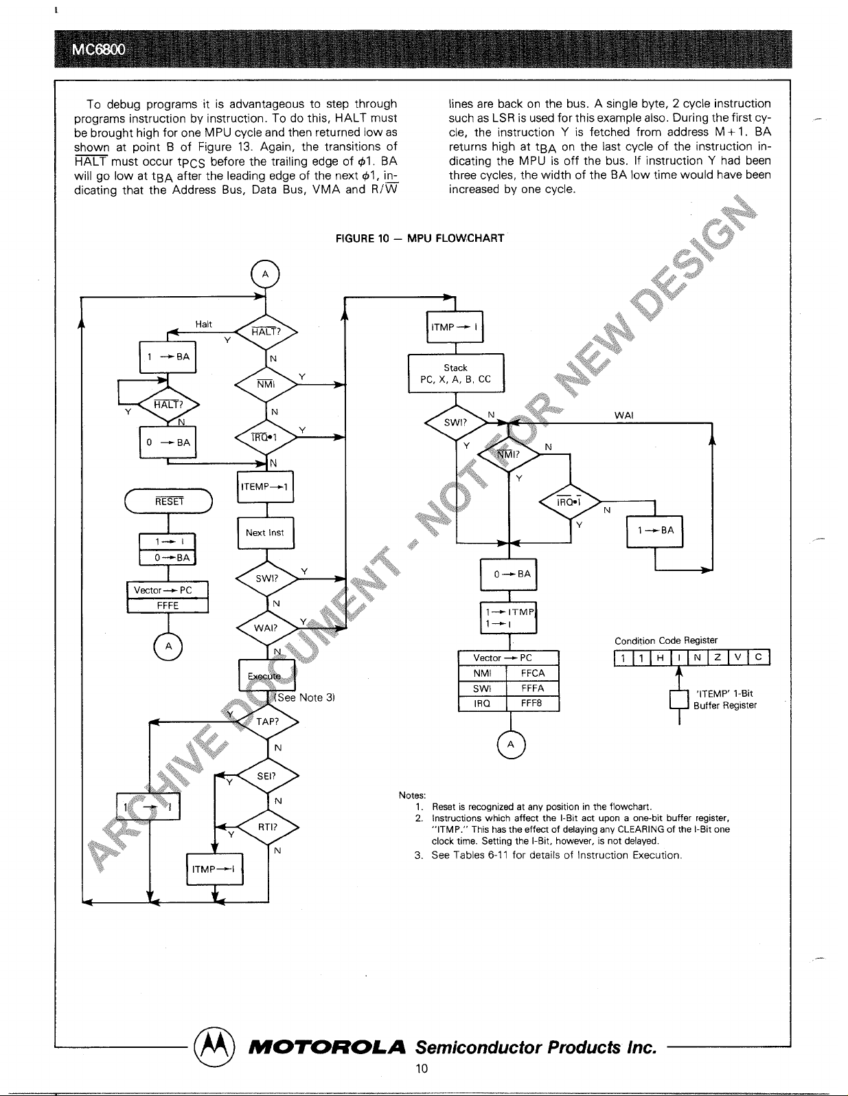
FIGURE 10 – MPU FLOWCHART
f
Y
1 +BA
3
Y
●
I 1
1.
2
3
0
A
Reset is recognized at any position in the flowchart.
Instructions which affect the l-Bit act upon a on~bh buffer register,
“lTMP.” This has the effect of delaying any CLEARING of the l-Bit one
clock time. Setting the l-Bit, however, is not delayed.
See Tables 6-11 for details of Instruction Execution.
m
MOTOROLA Semiconductor Products Inc.
10
Page 11

Address
Bus
R/R
VMA
Interrupt
IRQ or
m
Data Bus
BA
FIGURE 11 – WAIT INSTRUCTION TIMING
I
Cycle
I
I
I
I
I
I
I
I
I
#1
*
*
#4
*
&
#7
#8
*
#1 o
n
n+l
n+2
x
x
x
x
x x
x
Instruction
\
1[
x
x
x
x
x
x x
x
x
Wait Pc 0-7 PC 8-15
I 0-7
I B-15 ACCA
ACCB
New PC 8-15 New PC O-7
I nst
[[
Address Address
A
Note: Midrange waveform indicates
high
iMDedanCe state.
-TBA
FIGURE 12..+$tikE-STATE CONTROL TIMING
Page 12

1
@l
@z
m
BA
VMA
R/%
Address
Bus
Data
Bus
FIGURE13 – HALT AND SINGLEINSTRUCTION =ECUTION FORSYSTEM DEBUG
m
Instruction
Instruction Instruction
Fetch
Execute
\
/
XY
x
{1
))
x
XY
Fetch
Exwute
Addr M
x
.,
,
:.~~>),
The M PU has three 16-bit registers and thra-$,8~*@
registers available for use by the programmer (FJ$’@?~d@.
*.Y-I:,.,~~>,$
Program Counter – The program count~$&~?:’&t&o byte
(16 bits) register that points to the curre~~,”w~$m address.
,+$,‘~,i
Stack Pointer – The stack pon~*i~%,;&o byte register
that contains the address of the ne&,,a$ilable location in an
external push-down/pop-up st$~~$~fs stack is normally a
random access Read/Write,,,%b*~.#’’that may have any location (address) that is conV@ieJ~t. In those applications that
require storage of inf@~atidB’ In the stack when power is
lost, the stack muskl~~~~volatile.
,.,,,
$:.,,, ~?, ..
Index RWis~~~~~$%e index register is a two byte register
that is used x~i$~$?data or a sixteen bit memory address for
the lnde&& &&e of memory addressing.
;8 *
,.:,.
:$.,,,
{..... ..
..\..:+L.\:!!i,
Aq~$#~ators –
The MPU contains two 8-bit accwuktprs that are used to hold operands and results from
a~~{~~metic logic unit (ALU).
...
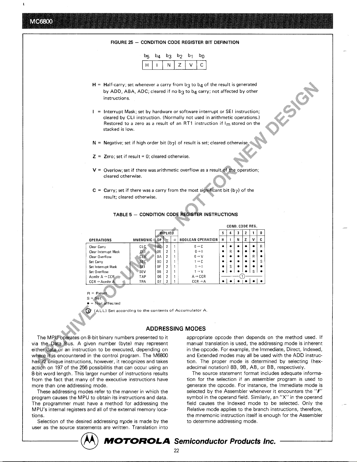
Condition Code Register – The condition code register in-
dicates the results of an Arithmetic Logic Unit operation:
Negative (N), Zero (Z), Overflow (V), Carry from bit 7 (C),
and half carry from bit 3 (H). These bits of the Condition
Code Register are used as testable conditions for the condi-
tional branch instructions. Bit 4 is the interrupt mask bit (l).
The unused bits of the Condition Code Register (b6 and b7)
are ones.
@
MOTOROLA
FIGURE14 – PROGRAMMING MODEL OF
THE MICROPROCESSINGUNIT
Pc
15
0
SP
7
m
llt
o
w
INZVC
Carrv (From Bit 7)
Overflow
Accumulator A
Accumulator B
Index Register
Program Counter
Stack Pointer
Condition Code
Registar
II
- zero
r ;:::t
Half Carrv (From Bit 3)
Semiconductor Products Inc.
12
-.
—.
Page 13

MPU INSTRUCTION SET
The MC~ instructions are described in detail in the When an instruction translates into two or three bytes of
MWW Programming Manual. This Section will provide a
code, the second byte, or the second and third bytes conbrief introduction and discuss their use in developing tain(s) an operand, an address, or information from which an
MC~ control programs. The MC66W has a set of 72 dif-
address is obtained during execution.
ferent executable source instructions. Included are binary
Microprocessor instructions are often divided into three
and decimal arithmetic, logical, shift, rotate, load, store, general classifications: (1) memory reference, so called
conditional or unconditional branch, interrupt and stack
because they operate on specific memory locations; (2)
manipulation instructions.
operating instructions that function without needing a
Each of the 72 executable instructions of the source
memory reference; (3) 1/0 instructions for transferring data
language assembles into 1 to 3 bytes of machine code. The between the microprocessor and peripheral devices. $+cl+
number of bytes depends on the particular instruction and In many instances, the M Cm performs the sarn”$*a-
on the addressing mode. (The addressing modes which are tion on both its internal accumulators and ~#r@rnal
available for use with the various executive instructions are
memory locations. In addition, the MC%:,~@terface
discussed later, ) adapters (PIA and ACIA) allow the MPU t~$~~~k~peripheral
The coding of the first (or only) byte corresponding to an
devices exactly like other memory loca@~$.3@#nce, no 1/0
executable instruction is sufficient to identify the instruction
instructions as such are required. Beca&Wq@these features,
and the addressing mode. The hexadecimal equivalents of
‘$,?~
other classifications are more sui~@fl~&~~b~introducing the
the binary codes, which result from the translation of the 72
MC66WS instruction set: (1) ,$cc’%hlator and
memory
instructions in all valid modes of addressing, are shown in operations; (2) Program cont~~t~perations; (3) Condition
Table 1. There are 197 valid machine codes, 59 of the 256
~ i~~~
Code Register operations, ,,,~~~~, %
possible codes being unassigned.
~~-~,,, ,.,,\.,
, ,\<!\{.i$’‘
~,,~:li
‘*+\.,~~i,
.t;~..
80
81
82
83
84
85
88
87
8a
a9
8A
aB
ac
8D
8E
8F
90
91
92
93
QA
SUB A
IMM
CMP A IMM
SBC A
IMM
AND A IMM
co
cl
C2
C3
C4
C5
ca
C7
C8
30
3112NOP
40
41
42
43
44
45
4a
47
48
49
4A
40
4C
4D
4E
4F
50
51
52
53
54
55
5a
57
5a
59
5A
5B
5C
5D
5E
5F
ao
NEG
COM
LSR
ROR
ASR
ASL
ROL
DEC
INC
TST
CLR
NEG
COM
LSR
ROR
ASR
ASL
ROL
DEC
INC
TST
A
A
A
A
A
A
A
A
A
A
A
B
B
B
B
B
B.
TAP
TPA
INX
DEX
BIT A IMM
LDA A IMM
Notes: 1 Addressing Modes:
A=
Accumulator A
B
= Accumulator B
REL = Relative
INO = Indexed
IMM =
Immetiate
DIR = Direc?
2. Unassign4 code indicated by J# * )‘.
EOR A IMM
IMM
IMM
IMM
IMM
IMM
OIR
DIR
DIR
DIR
DIR
DIR
DIR
DIR
DIR
DIR
DIR
DIR
DIR
IND
IND
IND
IND
IND
IND
IND
IND
IND
IND
IND
IND
IND
EXT
EXT
EXT
EXT
EXT
EXT
EXT
EXT
EXT
EXT
EXT
3A
3B
3C
?D
3E
3F
10
11
12
13
14
15
16
17
18
19
1A
IB
Ic
ID
IE
IF
20
21
22
23
24
25
2a
27
2a
29
CLV
SEV
CLC
SEC
CLI
SEI
SBA
CBA
B
B
B
B
B
B
B
B
B
B
B
B
B
B
B
B
B
B
B
B
B
B
B
B
B
B
B
a
B
B
B
B
B
a
CE LDX
CF .
DO SUB
01 CMP
D2
SBC
D3 “
D4
AND
D5
BIT
D6
LDA
D7
STA
Da EOR
D9
ADC
DA
ORA
DB ADD
DC ‘
DD .
DE LDX
DF
STX
EO SUB
El
CMP
E2
SBC
E3 .
E4 AND
E5 BIT
Ea
LDA
E7
STA
E8 EOR
E9 ADC
EA
ORA
EB ADD
EC .
ED .
EE
LDX
EF
STX
FO
SUB
F1
CMP
F2
SBC
F3 .
F4
AND
F5 BIT
F6 LDA
F7
STA
F8
EOR
F9
ADC
FA
ORA
FB ADD
FC “
FD .
FE
LDX
FF
STX
DIR
DIR
DIR
DIR
DIR
DIR
DIR
DIR
DIR
DIR
DIR
IND
[ND
IND
IND
IND
IND
IND
IND
lND
IND
IND
IND
IND
IND
IND
EXT
EXT
EXT
EXT
EXT
EXT
EXT
EXT
EXT
EXT
EXT
EXT
EXT
EXT
EXT
TAB
TBA A
A
A
A
A
A
A
A
A
A
A
A
A
A
A
A
A
A
A
A
A
A
A
A
A
A
A
DAA
ABA
9D
9E
9F
AO
Al
A2
A3
A4
A5
A6
A7
A8
A9
AA
AB
AC
AD
AE
AF
BO
B1
B2
B3
B4
LDS
STS
sua
BRA REL
REL
IND
CMP
SBCBHI
REL
REk
IND
INO
IND
INO
IND
IND
AND
BIT
LDA
STA
EOR
ADC
ORA
ADD
(ND
ac
INC
ao
TST
aE
JMP
6F CLR
70 NEG
71 .
72 .
73 COM
74 LSR
75 .
7a ROR
77 ASR
78 ASL
79 ROL
7A DEC
7B .
7C INC
7D TST
7E JMP
7F CLR
INO
IND
IND
IND
EXT
EXT
EX1
EXT
EX1
EX1
EX1
EX1
EX1
EX1
EX1
EX1
CPX
JSR
LDS
STS
SUB
CMP
SBC
32
PUL A
33
PUL B
34
DES
35
TXS
36
PSH A
37
PSH B
38 .
AND
BIT
LDA
STA
EOR
ADC
ORA
ADD
CPX
JSR
B5
Ba
B7
Ba
B9
BA
BB
BC
BD
BE
BF
39 RTS
3A “
3B
RTI
3C “
3D .
3E
WAI
3F Swl
LOS
STS
EXT
EXT
m
MOTOROLA Semiconductor Products Inc.
13
Page 14

1
----- -
. . . . . .... ---- . ... . .. ... . .. ---- .-,-. ,-
lABLt Z — ALUUMULAIUR AND MtMUMY UrErnAt IUN>
OPERATIONS
MNEMONIC
Add
Add Acmltrs
Add wlfh Carry
And
Blt Tesl
Clear
Compare
Compare Acmltrs
Complement, 1’s
Complement, 2’s
(Negate)
Dec!mal Adi.st, A
Decrement
ExcI”si”e OR
Increment
Load Acmltr
Or, Inclusive
Push Oata
Pull Oata
Rotate Left
Rotate R,ght
Shift Left, Ar!thmet!c
Sh[ft Right, Arfthmet!c
Sh!f! Right, Logic
Store Acmltr.
Subtract
Subtracf Acmltrs.
ADDA
ADOB
ABA
AOCA
AOCB
ANDA
ANOB
BITA
BITE
CLR
CLRA
CLRB
CMPA
CMPB
CBA
COM
COMA
COMB
NEG
NEGA
NEGB
OAA
OEC
oECA
OECB
EORA
EORB
INC
INCA
INCB
LOAA
LDAB
O RAA
ORAB
PSHA
?SHB
PU LA
PU LB
ROL
ROLA
ROLB
ROR
RORA
RORB
ASL
ASLA
ASLB
ASR
ASRA
ASRB
LSR
LSRA
LSRB
Arithmetic Minus;
Boolean ANO:
MSP contents Of memow location pointed to be Stack Pointer:
Boolean Inclusive OR;
&
Boolean Exclusive OR;
M
Complement of M;
+
Transfer Into;
o
Bit = Zero;
00 Byte = Zero;
AOORESSING MOOES
EXTNO
INOEX
1P-=
CON OtTION CODE SYMBOL5
H
Half.carrv from bit 3;
I Interrupt mask
N Negative (tign bit)
z Zero (byte)
v
Ovetilow, 2’s complement
c Carv from bit 7
R
Rewt Always
s
Set Alwav$
IMPLIEO
1P-=
B21
F21
F21
121
1321
i321
lo2f
io21
1921
IA21
,A21
1C21
iC21
!9 2
j9 2
!6 2
j6 2
$8 2
58 2
a7 2
57 2
44 2
54 2
10 2
16 2
17 2
$0 2
50 2
1
1
1
I
1
1
1
1
1
1
1
1
1
1
1
I
1
1
1
—
BOOLEAN/ARITHMETIC OPERATf ON
(All register labels
refer to contents)
A+ M-A
B+M+B
A+ MSp, SP-f-SP
B-, Msp, SP–l+SP
SP+I-SP, MSP-A
SP+I+SP, MSP-B
M
A
B
}L-’’’’””J
c
b7 - bO
M
A
B
lk-’’’’”[d
c b7 — bO
M
A}o-~ - 0
B
b7
bO C
A’-M
B-M
A– M-A
B– M-B
A– B-A
A–M– C-A
B- M– C-B
A-B
B-A
M–00
A–00
B–DO
CON OITION COOE REGISTER NOTES:
(Bit Set if testis true and cleared otherwise]
1
(Bit
V) Test: Result = 1000OOOO7
2
(Bit C) Test: Result = 000000007
3
(Bit C) Test: Oecimal value of most significant BCO
Character greater than nine?
( Not cleared if previously set.]
4
(Bit V) Test: Operand= 10000000 prior to execution?
5 (Bit V) Test: Operand= 01111111 prior to execution?
t Test and set if true, cleared otherwise
6 (Bit V) Test: Set equal to result of N@C after shift has occurred
●
Not Affected
Note – Accumulator addresbng mode instructions are included in tho column for IMPLIEO addressing
@
MOTOROLA Semiconductor Products Inc.
14
.-
.—
-.
Page 15

PROGRAM CONTROL OPERATIONS
Program Control operation can be subdivided into two
categories: (1) Index Register/ Stack Pointer instructions; (2)
Jump and Branch operations.
Index Register/ Stack Pointer Operations
The instructions for direct operation on the MPU’S Index
Register and Stack Pointer are summarized in Table 3.
Decrement (DEX, DES), increment (INX, INS), load (LDX,
LDS), and store (STX, STS) instructions are provided for
both. The Compare instruction, CPX, can be used to compare the Index Register to a 16-bit value and update the Con-
dition Code Register accordingly.
The TSX instruction causes the Index Register to be load-
ed with the address of the last data byte put onto the
“stack. ” The TXS instruction loads the Stack Pointer with a
value equal to one less than the current contents of the Index
Register. This causes the next byte to be pulled from the
“stack” to come from the location indicated by the index
Register. The utility of these two instructions can be clarified
by describing the “stack” concept relative to the M@W
system.
The “stack” can be thought of as a sequential list of data
stored in the MPU’S read/write memory. The Stack Pointer
contains a 16-bit memory address that is used to access the
list from one end on a last-in-first-out (LIFO) basis in contrast
to the random access mode used by the MPU’S other addressing modes.
The MC~ instruction set and interrupt structure allow
extensive use of the stack concept for efficient handling of
data movement, subroutines and interrupts. The instructi~.os
can be used to establish one or more “stacks” anywhg~~~<
read/write memory. Stack length is limited only <,q~$~~e
amount of memory that is made available.
.,is,~
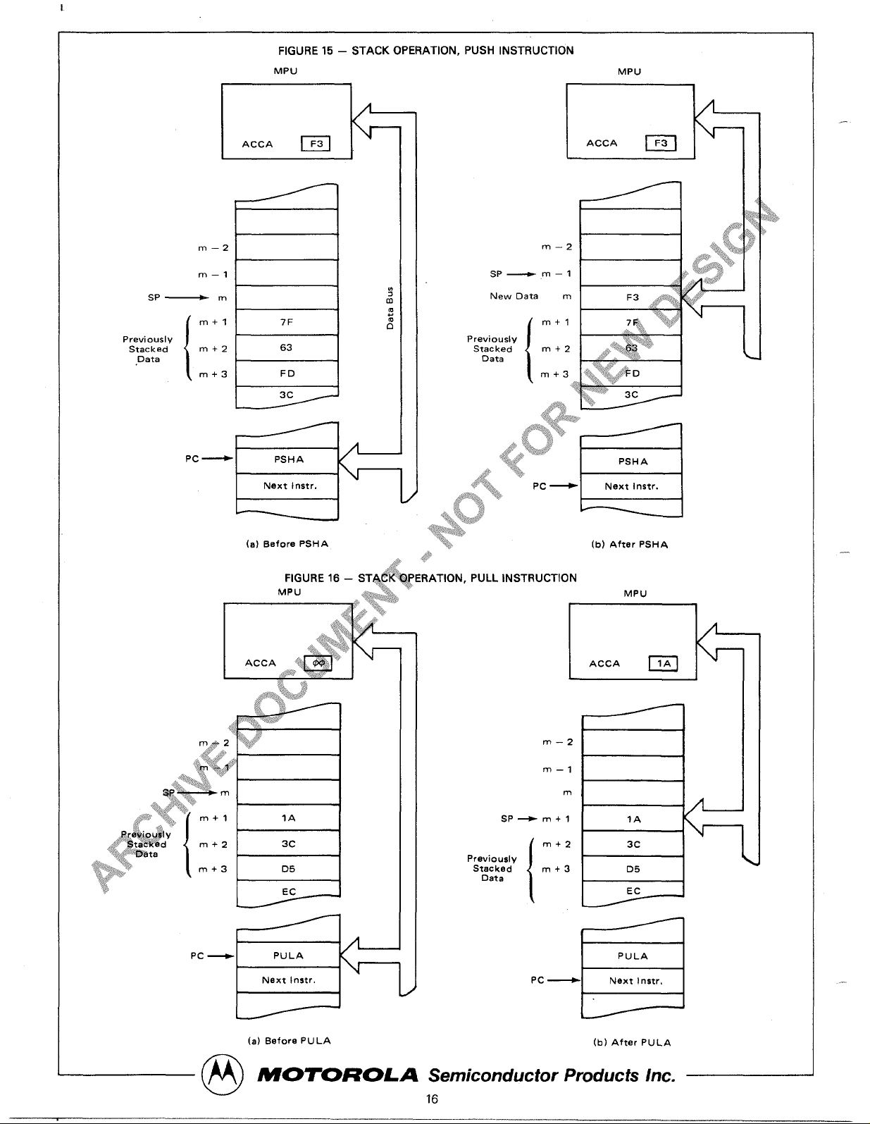
,.,
Operation of the Stack Pointer with the Pus@,@i~~,Rtillinstructions is illustrated in Figures 15 and 1~~..%~.$ush instruction (PSHA) causes the contents of kd$~~icated accumulator (A in this example) to be stor~+in;wemory at the
location indicated by the Stack Point@r. ~Q&Stack Pointer is
automatically decremented by ~~~~$~t~wing the storage
operation and is “pointing” to th~~:~e{$empty stack location.
The Pull instruction (PULA ..@~:~%’B) causes the last byte
stacked to be loaded intothe:w’ropriate accumulator. The
Stack Pointer is automatically incremented by one just prior
to the data transfer so that it will point to the last byte stacked rather than the next empty location. Note that the PULL
instruction does not “remove” the data from memory; in the
example, 1A is still in location (m+ 1) following execution of
PULA. A subsequent PUSH instruction would overw~jt~~at
location with the new “pushed” data.
‘..$.,,,.$,.*,.,,.:
i:~).:~
~.f.,k\,
Execution of the Branch to Subroutine (BSR)a$d. #~rrfp to
Subroutine (JSR) instructions cause a returD%~*~ to be
saved on the stack as shown in Figures
18$~w~@ 20. The
stack is decremented after each byte of,.#$r@?n address is
pushed onto the stack. For both of$&~~N@structions, the
return address is the memory locatid~ f~jo’wing the bytes of
code that correspond to the B,S$.:an’~:$&SRinstruction. The
code required for BSR or J
g~g”~<y be either two or three
bytes, depending on whet~r,%~.J SR is in the indexed (two
bytes) or the extende~$~$~$@ bytes) addressing mode.
Before it is stacked, t@<&~$Yam Counter is automatically in-
cremented the correct Rgmber of times to be pointing at the
location of the ~$~~~$truction. The Return from Subroutine
lnstruction,,,@K$~~puses the return address to be retrieved
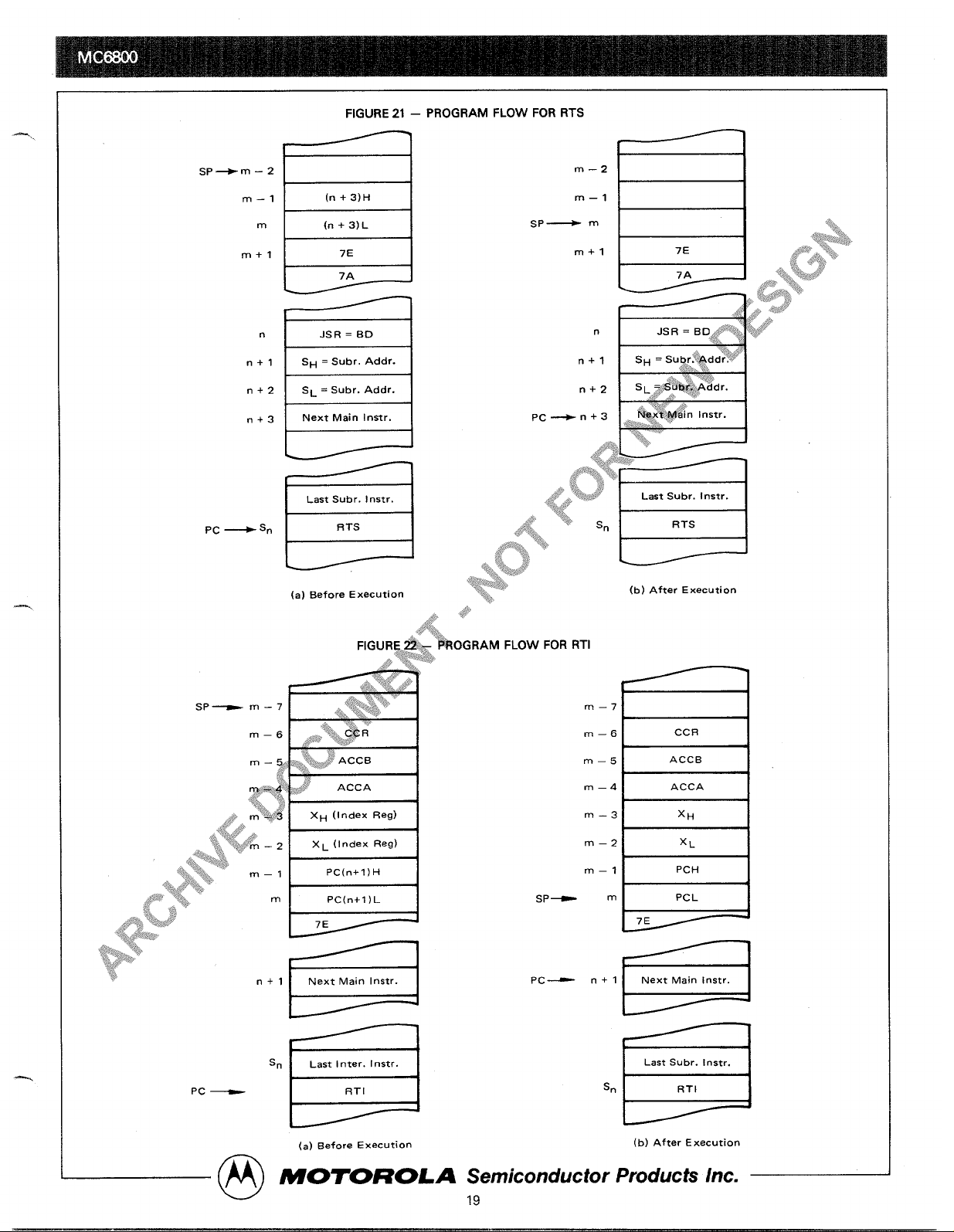
and Ioade@I$to t~e Program Counter as shown in Figure 21.
There $r~s~$eral operations that cause the status of the
M PU.,$0b$wved on the stack. The Software Interrupt (SWI)
and$%ait for Interrupt (WAI) instructions as well as the
~?~,ah~e (~Q) and non-maskable (N MI) hardware inter-
-$ ‘~~@J&all cause the M PU’S internal registers (except for the
,.,,,:f?
*,..~,@tack Pointer itself) to be stacked as shown in Figure 23.
“$k MPU status is restored by the Return from Interrupt, RTI, as
,,\.
shown in Figure 22.
Jump and Branch Operation
The Jump and Branch instructions are summarized in
Table 4. These instructions are used to control the transferor
operation from one point to another in the control program.
The No Operation instruction, NOP, while included here,
is ajump operation in a very limited sense. Its only effect is to
increment the Program Counter by one. It is useful during
program development as a “stand-in” for some other instruction that is to be determined during debug. It is also used for equalizing the execution time through alternate paths
in a control program.
!*,. .s. .
,
‘:.
?::r~~~,,,t>~i*,
?..*
.t
‘*:Z
!$s.
iMMED DIRECT
PO 1NT$&Q$~&&?10 NS
MNEMONIC OP - = OP -
~
Co mp%~$~:her Reg
CPX
8C 3 3 9C 4
2
o~eq~,:~$ndex Reg
OEX
Oe~.~efit Stack Pntr O ES
lnc;&ment Index Reg INX
Increment Stack Pntr INS
Load Index Reg LOX
CE 3
3 OE 4
2
Load Stack Pntr LOS
8E 3 3
9E 4
2
Store Index Reg STX
DF 5
2
Store Stack Pntr STS
9F 5
2
Indx Reg +Stack Pntr TXS
Stack Pntr * Indx Reg
TSX
OP
—
AC
EE
AE
EF
AF
62
1
62
62
72
72
f
OP
Bc
FE
BE
FF
BF
(TNO
5
5
6
6
IMPLIEO I
—
OP
—
09
34
08
31
35
30
—
—
—
4
4
4
4
4
4
—
~
BOOLEAN/ARITHMETIC OPERATION
1
1
1
1
I
L
1
1
X–l+x
SP–1-SP
X+l+x
SP+l+SP
MA XH, (M+l) -XL
M+ SPH, (M+1)4SPL
XH+M, XL+(M+l)
SPH+M, SPL~(M+l)
X-1-SP
SP+l+X
@ (Bit N) Test: Sign bit of most significant (MS) byte of result= 1?
@ (Bit V) Test: 2s complement o“erfiow from subtraction of m. byte.?
@ (Bit N) Test: Result Iesstha” zero? (Bit 15= 1)
@
MOTOROLA Semiconductor Products Inc. —
15
I
CO ND. COOEREG
Page 16
I
FIGURE 15 – STACK OPERATION, PUSH INSTRUCTION
SP~m
.{EI
m+l
7F
Previously
Stacked
m+2
63
Data
m+3
FD
‘c--
(a) Before PSHA
MPU
m
~’q..i,
%
(b) Aftar PSHA
Pc ~
PULA
Next In$tr.
MPU
I I
I
ACCA m
I
m—2
m—1
m
SP+m+l
{
mt2
Previously
Stacked m+3
Data
I
1A
3C
D5
\
P
(b) After PULA
(a) Before PULA
m
MOTOROLA Semiconductor Products Inc.
16
—
—
Page 17
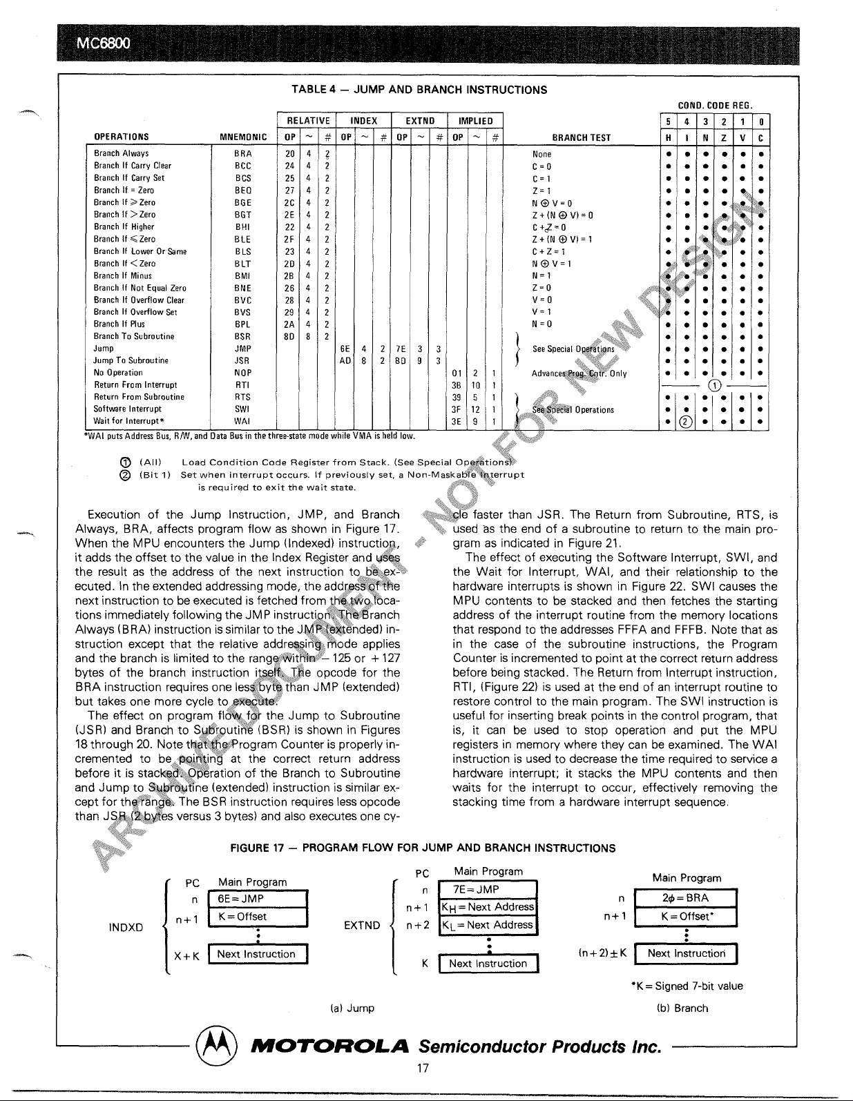
TABLE 4 – JUMP AND BRANCH INSTRUCTIONS
hl
—
Y
4
4
4
4
4
4
4
4
4
4
4
4
4
4
8
—
‘n
T
—
#
T
2
2
2
2
2
2
2
2
2
2
2
z
2
2
2
~
—
G
—
6E
AO
m
RE
OPERATIONS
Branch Always
Branch If Carry Clear
Branch If Carry Set
Branch If = Zero
Branch If > Zero
Branch If >Zero
Branch If Higher
Branch If < Zero
Branch If Lower Or Same
Branch If < Zero
Branch If Minus
Branch If Not Equal Zero
Branch If Overflow Clear
Branch If Ovefilow Set
Branch If Plus
Branch To Subroutine
Jump
Jump To Subroutine
No Operation
Return From Interrupt
Return From Subroutine
Softwre Interrupt
Wait for Interrupt%
IAI puts Address Bus, RN, and
@ (All)
—
~ (Bit 1) Set when interrupt occurs. if previously set, a Non-MaSk,:~e’’%?errUPt
MNEMONIC
BRA
BCC
BCS
BEO
BGE
BGT
BHI
BLE
B LS
B LT
BMI
BNE
BVC
BVS
BPL
BSR
JMP
JSR
NOP
RTI
RTS
G
G
24
25
27
2C
2E
22
2F
23
20
2B
26
28
29
2A
80
Swl
WAI
ita Businthet
Load Condition Code Register from Stack. (See Special Op$@tic
is required to exit the wait state.
~
—
i
—
—
#
—
—
3
3
9
3
—
—
low
.*
~+. ‘~
L
I
I
I
I
I
..?
BRANCH TEST
CONO. COOE REG.
T
10
Vc
Execution of the Jump Instruction, JMP, and Branch
Always, BRA, affects program flow as shown in Figure 17.
When the MPU encounters the Jump (Indexed) instruction,
it adds the offset to the value in the Index Register and %,
the result as the address of the next instruction to~b~;~x~$
ecuted. In the extended addressing mode, the add[e~~~?he
next instruction to be executed is fetched from
immediately following the JM P instructl~~~}K~WBranch
tions
Always (BRA) instruction is similar to the J~~?~#~&nded) in-
,$~$~*~~ca-
struction except that the relative addre&Sin&. fiode applies
and the branch is limited to the rang~Wtkm$- 125 or + 127
bytes of the branch instruction i~$~}%%.~~e opcode for the
BRA instruction requires one les$by~ than J M P (extended)
but takes one more cycle to @?
The effect on program
(JSR) and Branch to
Sw#rQu{*$ (BSR) is shown in Figures
~4,i..‘..,,..\.?,,$<‘
fl~~ f$r the Jump to Subroutine
18 through 20. Note t~%:$@Program Counter is properly incremented to be$:~~~:n~ at the correct return address
before it is stac~&i,;~~#~ration of the Branch to Subroutine
and Jump to a~w~’tine (extended) instruction is similar except for th@~~n~&>The BSR instruction requires less opcode
than J $$&R{%Q~#esversus 3 bytes) and also executes one cy -
FIGURE 17 – PROGRAM FLOW FOR JUMP AND BRANCH INSTRUCTIONS
‘+~’$..used as
~y:
gram as indicated in Figure 21,
the end of a subroutine to return to the main pro-
The effect of executing the Software Interrupt, SWI, and
the Wait for Interrupt, WAI, and their relationship to the
hardware interrupts is shown in Figure 22. SW! causes the
M PU contents to be stacked and then fetches the starting
address of the interrupt routine from the memory locations
that respond to the addresses FFFA and FFFB. Note that as
in the case of the subroutine instructions, the Program
Counter is incremented to point at the correct return address
before being stacked. The Return from Interrupt instruction,
RTI, (Figure 22) is used at the end of an interrupt routine to
restore control to the main program. The SWI instruction is
useful for inserting break points in the control program, that
is, it can be used to stop operation and put the MPU
registers in memory where they can be examined. The WAI
instruction is used to decrease the time required to service a
hardware interrupt; it stacks the MPU contents and then
waits for the interrupt to occur, effectively removing the
stacking time from a hardware interrupt sequence,
[X+K~ [ ,,-, (n+2)*Klxl
●K = Signed 7-bit value
(a) Jump
m
MOTOROLA Semiconductor Products Inc.
17
(b) Branch
Page 18
I
FIGURE 18 – PROGRAM FLOW FOR BSR
a
(n +2)H
-.
SP~m–2
m—1
m
m+l
n
n+l
n+2
“ + 1 ] tK = Offset* I
n+ 2 I Next Main l“str. I
* K = Signed 7-Bit value
(a) Before Execution
,~i)::~’
\ ,\~.,,
FIGURE 19 – PROGRAM FLOW FOR JSR (~TENDEm,\ ‘%,
FIGURE 20 – PROGRAM FLOW FOR JSR (lNDWED)
r
m—1
(n+2)H
m
(n+2)L
m+l 7E
7A
—
m—l
sP—m
m+l
B
7E
7A
PC_n
a
JSR=AD
n+l K = Of fset”
“+2
Next Main l“str.
“
g
JSR = AD
“+1
K = Offset
“+2
Next Main l“str.
“1
JS R
I
n+ 2 I SL=Sub,. Addr, I
●K = 8-Bit U“sig”ed Value
PC+ X.+K
1st S.br, Instr.
1
r
1
(a) Before Ex%utton
““s=
“Contents of Index Register
(a) Before Execution
(b) Afrer Execuxion
(S formed from
SH and SL) 1
(b) After Execution
MOTOROLA
Semiconductor Products Inc.
18
Page 19
SP-m–2
m—1
m
m+l
n
n+l
nt2
nt3
FIGURE 21 – PROGRAM FLOW FOR RTS
H
m—2
(n+3)H m—1
SH = Subr. Addr.
n+l
SL = Subr. Addr.
n+2
I
B
Last Subr. Instr.
R TS
Pc —
J
s“
a
Last Inter. Instr.
RTI
FLOW FOR RTI
m—7
m—6
m—5
m—4
m—3
m—2
m—1
sp~ m
Pc—
“+1
s“
CCR
ACCB
ACCA
x~
XL
PCH
4
PCL
7E
I Next Main I“str. I
I Last S“br. Instr. I
(a) Before Execution
(b) After Execution
@
MOTOROLA Semiconductor Products Inc.
19
Page 20
I
FIGURE ~ – PROGRAM FLOW FOR INTERRUPTS
Wait For
Hardware Interrupt or
Interrupt
NonMaskable Interrupt (NMI)
.-
Software lnterruDt
Main Program’
n:=.
Main Program
Main Program
:1= n-
7“
Sp +
Stack MPU
Register Contents
m—7
m—6
m—5
m—4
m—3
m—2
m—1
m
WI
FFF8
FFFC
FFF9
FFFD
FFFE
FFFF
d
Set Interrupt
Mask (CCR4)
Interrupt Memorv Assignment
FFF8
I
IRQ
I
Ms
FFF9
IRQ
LS
FFFA
Swl
MS
FFFB
Swl
LS
#
First Instr.
e BvFetching
Addr. Formed
Q
Load Interrupt
Vector Into
2.Eytes From
Program Counter
Per, Mere,
Assign.
f
A
Interruot Proaram
>
,.
1 lstlnterruutlnstr.
1
NOTE: MS= Most Significant Address Bvte;
LS = Least S~nificant Address Byte;
I
1
@
MOTOROLA Semiconductor Products Inc.
20
Page 21
FIGURE 24 – CONDITIONAL BRANCH INSTRUCTIONS
BMI : N=l ;
BEQ :
Z=l ;
BPL :
N=@ ;
BNE :
Z=4 ;
BVC :
V=$ ;
BCC :
C=$ ;
BVS : V=l ;
BCS :
C=l ;
BHI :
c+ z=@ ;
BLT :
N@V=l ;
BLS :
C+z=l ;
BGE :
N@ V=@ ;
BLE :
Z+(N@V)=l
BGT :
Z+(N@V)=@ ;
The conditional branch instructions, Figure 24, consists of
seven pairs of complementary instructions. They are used to
test the results of the preceding operation and either continue with the next instruction in sequence (test fails) or
cause a branch to another point in the program (test succeeds).
Four of the pairs are used for simple tests of status bits N,
Z, V, and C:
1. Branch on Minus (B MI) and Branch On Plus (BPL) tests
the sign bit, N, to determine if the previous result was
negative or positive, respectively.
2. Branch On Equal (BEQ) and Branch On Not Equal
(BNE) are used to test the zero status bit, Z, to determine
whether or not the result of the previous operation was equal
to zero. These two instructions are useful following a Compare (CMP) instruction to test for equality between an accumulator and the operand. They are also used following the
Bit Test (BIT) to determine whether or not the same bit pos~~
tions are set in an accumulator and the operand.
>.t;.’:
,Y).....,.,,~
3. Branch On Overflow Clear (BVC) and Branc@$~ns
Overflow Set (BVS) tests the state of the V bit to ~&~*e
if the previous operation caused an arithmetic Q@r,@~
4. Branch On Carry Clear (BCC) and Branch
@~b$rY Set
(BCS) tests the state of the C bit to determ~~$$~~~previous
operation caused a carry to occur. BCC ~~,~~~b are useful
.,*.J?,’
-~>,‘:?
CONDITION
for testing relative magnitude when the values being tested
are regarded as unsigned binary numbers, that is, the values
are in the range 00 (lowest) to FF (highest). BCC following a
comparison (CMP) will cause a branch if the (unsigned)
value in the accumulator is higher than or the same as the
value of the operand. Conversely, BCS will cause a branch if
the accumulator value is lower than the operand.
The fifth complementary pair, Branch On Higher (Qi&~~~,nd
Branch On Lower or Same (BLS) are, in a se~https://manualmachine.com/~@~plements to BCC and BCS. BHI tests for both C ~n@~~O; if
used following a CMP, it will cause a branc~,?k~~pWalue in
the accumulator is higher than the oper&~~%50nversely,
BLS will cause a branch if the unsignq~’~~a~’”value in the
accumulator is lower than or the saW:~$J&b operand.
The remaining two pairs are u~~l ~ ‘testing results of
operations in which the values at% re&~Yded as signed two’s
complement numbers. This $%&&}{rom the unsigned binary
case in the following sen:~+~~.{~nsigned, the orientation is
higher or lower; in si~w’~,wo’s complement, the comparison is between @$~~g~&~ smaller where the range of
values is between – 1~,.,and + 127.
Branch On L@$~$anZero (BLT) and Branch On Greater
Than Or Eq~#k.~~~’~~G E) test the status bits for N @V= 1
and N e V{~$<,,r~pectively. B LT will always cause a branch
followin$~~s 8~~ration in which two negative numbers were
adde,~. in’~dition, it will cause a branch following a CMP in
wh#~$Jhe value in the accumulator was negative and the
,@$&~~n’&was positive. B LT will never cause a branch follow-
.,:t~@,$#CMP in which the accumulator value was positive and
,,+,. we operand negative. BGE, the complement to BLT, will
{f$:,,.j..::}
‘*N cause. a branch following operations in which two positive
,+::>
values were added or in which the result was zero.
The last pair, Branch On Less Than Or Equal Zero (BLE)
and Branch On Greater Than Zero (BGT) test the status bits
for Z@ (N+V) = 1 and Z@ (N +V) =0, respectively. The action of BLE is identical to that for BLT except that a branch
will also occur if the result of the previous result was zero,
Conversely, BGT is similar to BGE except that no branch will
occur following a zero result.
CODE REGISTER
‘ i$,:,i;;*
,,,1.,. . .
.,.y ~
OPERATIONS
..?“s$.~$$:’,,
‘$?.,,
l~~k,J.F
The Condition ~~~~Register (CCR) is a 6-bit register
to precede any SEI instruction with an odd opcode – such
within the MPU~~~kl$*useful in controlling program flow
as NOP. These precautions are not necessary for MC~
during system d;%tlon. The bits are defined in Figure 25.
processors indicating manufacture in November 1977 or
The instr~~lia~% shown in Table 5 are available to the user
later.
for dire~#~@@@ulation of the CCR.
Systems which require an interrupt window to be opened
A C~,$A/ instruction sequence operated properly, with
under program control should use a CLI-NOP-SEI sequence
earl~:~~$~~ processors, only if the preceding instruction
rather than CLI-SEI.
was $~d (Least Significant Bit= 1), Similarly it was advisable
@
MOTOROLA Semiconductor Products Inc.
21
Page 22
L
CO ND. COOE REG.
E
= BOOLEAN OPERATION
1 O+c
1 0+1
1 O+v
1
l+C
1 1+1
1
l-v
1
A+CCR
1 CCR+A
m
HI NZVC
● 00m*
R
●
R****
● .mm
R.
● Ore**
s
●
S. *Q.
● **O
s.
w
● ● ● \* ● ●
The M P&%~&$ates on 8-bit binary numbers presented to it
via the..~t~~~?{~us. A given number (byte) may rePresent
eithe&~{~~@:or an instruction to be executed, depending on
w@.@/~,~s encountered in the control program. The Mm
ha$~~tinique instructions, however, it recognizes and takes
actloh on 197 of the 256 possibilities that can occur using an
8-bit word length. This larger number of instructions results
from the fact that many of the executive instructions have
more than one addressing mode.
These addressing modes refer to the manner in which the
program causes the MPU to obtain its instructions and data.
The programmer must have a method for addressing the
MPU’S internal registers and all of the external memory loca-
tions.
Selection of the desired addressing mode is made by the
user as the source statements are written. Translation into
@
MOTOROLA
appropriate opcode then depends on the method used. If
manual translation is used, the addressing mode is inherent
in the opcode. For example, the immediate, Direct, Indexed,
and Extended modes may all be used with the ADD instruction. The proper mode is determined by selecting (hexadecimal notation) 8B, 9B, AB, or BB, respectively.
The source statement format includes adequate information for the selection if an assembler program is used to
generate the opcode. For instance, the Immediate mode is
selected by the Assembler whenever it encounters the “#”
symbol in the operand field. Similarly, an “X” in the operand
field causes the Indexed mode to be selected. Only the
Relative mode applies to the branch instructions, therefore,
the mnemonic instruction itself is enough for the Assembler
to determine addressing mode.
Semiconductor Products Inc. ~
22
—.
Page 23
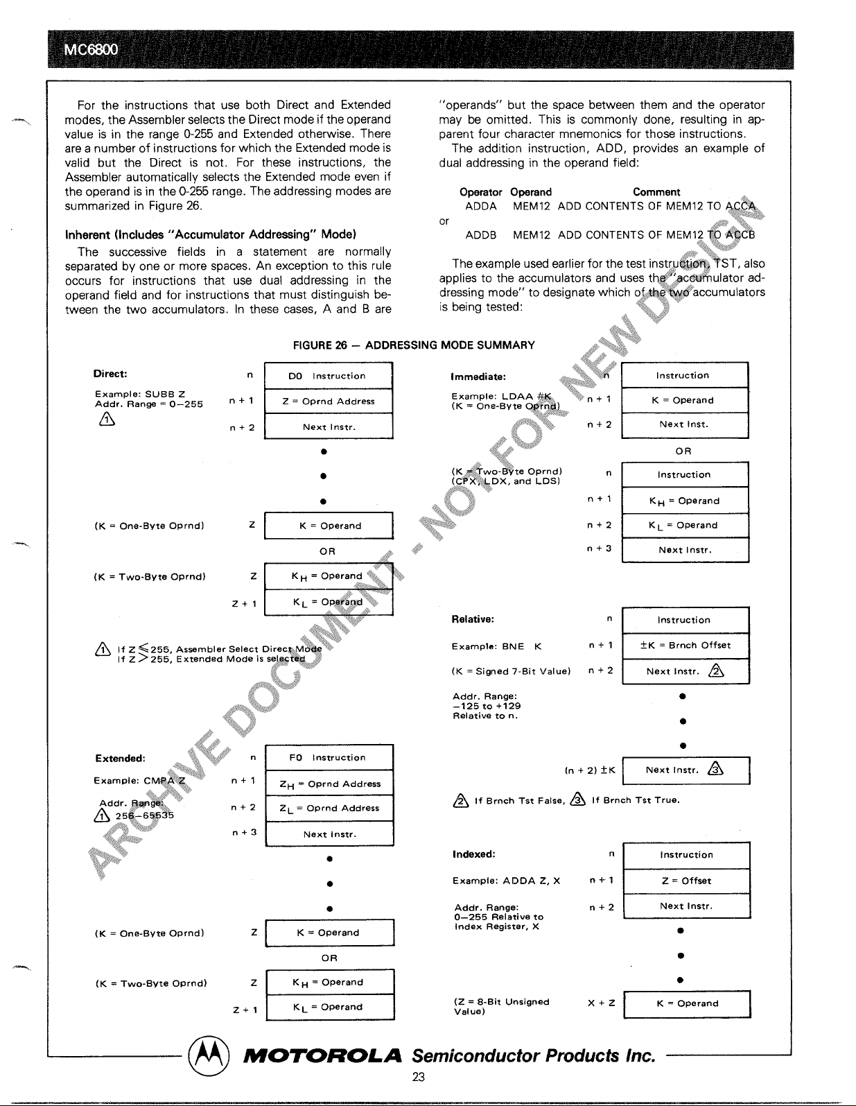
For the instructions that use both Direct and Extended
“operands” but the space between them and the operator
modes, the Assembler selects the Direct mode if the operand
may be omitted. This is commonly done, resulting in ap-
vaiue is in the range O-255 and Extended otherwise. There
parent four character mnemonics for those instructions.
are a number of instructions for which the Extended mode is
The addition instruction, ADD, provides an example of
valid but the Direct is not. For these instructions, the
dual addressing in the operand field:
Assembler automatically selects the Extended mode even if
the operand is in the O-255 range. The addressing modes are
Operator Operand
Comment
summarized in Figure 26.
ADDA MEM12 ADD CONTENTS OF MEM12 TO j&~$:k
or
.t;..,
Inherent (Includes “Accumulator Addressing” Mode)
~~,~~1~$~,,?~..:$
ADDB MEM12 ADD CONTENTS OF MEM12 %Q #&C~
The successive fields in a statement are normally
i.;~:,
,,,~ ,;i,\.JtJ$+t’$
separated by one or more spaces. An exception to this rule
The example used earlier for the test instru~&~~?ST, also
occurs for instructions that use dual addressing in the
applies to the accumulators and uses th,$~~~~ohulator adoperand field and for instructions that must distinguish re-
dressing mode” to designate which o$,,x’v-accumulators
tween the two accumulators. In these cases, A and B are
is being tested:
\,*\
~$.;:
.~#<:,\,~:;
.jt
.\~;,
. .
Direct:
n
DO Instruction
Example: SUBB Z
Addr. Rane = O–255
A
n+l
Z = Oprnd Address
n+2 Next Instr.
(K = One-Bvte Oprnd)
●
z&
OR
.:,,.
(K = Two-Bvte Oprnd)
(K = One-Bvte Oprnd)
(K = Two-Bvte OPrnd)
J
ntl
ZH = Oprnd Addr-s
n+2
ZL = Oprnd Address
n+3
Next Instr.
.
●
z&
OR
z
[
KH = Operand
I
*“r,
n+2 Next Inst.
OR
n+2
I
KL = Operand
I
n+3
I
Next Instr.
I
Relative:
n
I
Instruction
I
Example: BNE K
(K = Signed 7-Bit Value)
Addr. Range:
–125t0 +129
Relative to n.
●
●
(“+2)’K-
~ If Br”ch Tst False, ~ if Brnch Tst True.
Indexad:
n
Instruction
I
Example: ADDA Z, X
‘+1-
Addr. Range:
n+2
I
Next Instr.
O–255 Relative to
1
Index Register, X
o
●
(Z = a-Bit Unsignad
Value)
x+z&
@
MOTOROLA Semiconductor Products Inc.
Q9
Page 24
1
* :’@o
Operator
Comment
mode, the “address” of the operand is effectively the
TSTB TEST CONTENTS OF ACCB
memory location immediately following the instruction itself.
or
Table 7 shows the cycle-by-cycle operation for the im-
TSTA TEST CONTENTS OF ACCA
mediate addressing mode.
A number of the instructions either alone or together with
Direct and Extended Addressing Modes – In the Direct
an accumulator operand contain all of the address informa-
tion that is required, that is,
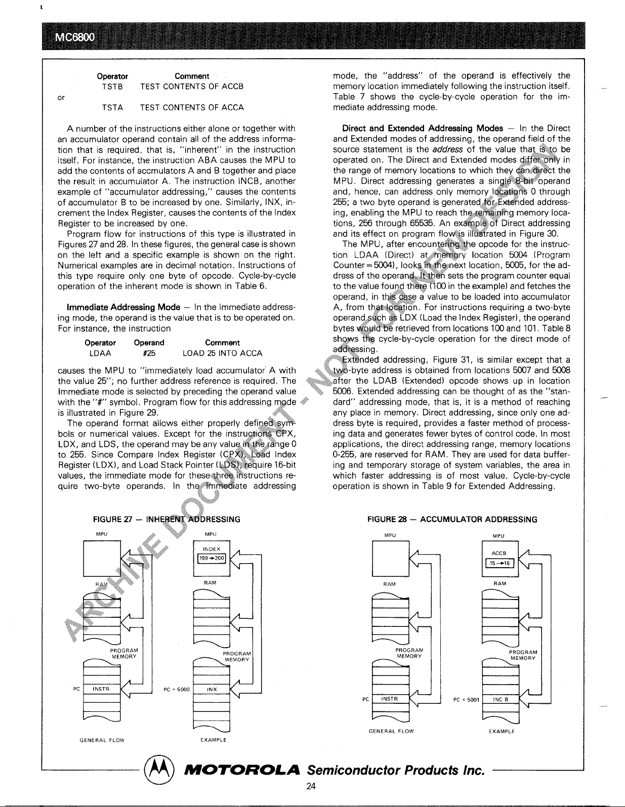
“inherent” in the instruction
itself. For instance, the instruction ABA causes the MPU to
add the contents of accumulators A and B together and place
the result in accumulator A. The instruction INCB, another
example of “accumulator addressing,” causes the contents
of accumulator B to be increased by one. Similarly, INX, increment the Index Register, causes the contents of the Index
Register to be increased by one.
Program flow for instructions of this type is illustrated in
Figures 27 and 28. In these figures, the general case is shown
on the left and a specific example is shown on the right.
Numerical examples are in decimal notation. Instructions of
this type require only one byte of opcode. Cycle-by-cycle
operation of the inherent mode is shown in Table 6.
Immediate Addressing Mode – In the Immediate addressing mode, the operand is the value that is to be operated on.
For instance, the instruction
Oper*or Operand
Comment
LDAA #25
LOAD 25 INTO ACCA
causes the M PU to “immediately load accumulator A with
the value 25’; no further address reference is required. The
Immediate mode is selected by preceding the operand value
with the “#” symbol. Program flow for this addressing m,~de
is illustrated in Figure 29.
y..\
.*.,.J.$,i~>>,
The operand format allows either properly define$:$ym
bols or numerical values. Except for the instru~ti~~’WX,
LDX, and LDS, the operand may be any valu~,i~:~e,;~nge O
to 255. Since Compare Index Register (C&,~Q$.~~&’d Index
Register (LDX), and Load Stack Pointer (~$~;.$e~uire 16-bit
values, the immediate mode for these~%re~+ ~tistructions require two-byte operands. In th~:T~,Yate addressing
4
PROGRAM
MEMORY
Pc
INSTR
GENERAL FLOW
PC = 5000
MPu
@
INDEX
a
RAM
z
PROG RAM
MEMORY
INX
t I
EXAMPLE
and Extended modes of addressing, the operand field of the
source statement is the address of the value tha$+i$j~o be
operated on. The Direct and Extended modes d~ff~$:fi$y in
the range of memory locations to which they ~$~~trect the
M PU. Direct addressing generates a sin~l~.~~%~ operand
and, hence, can address only memory l@~&&~’& O through
255; a two byte operand is generated~{&~QEx&&~ded addressing, enabling the MPU to reach theik~~~J&”hg memory locations, 256 through 65535. An ex~&pl$ O* Direct addressing
and its effect on program flo,~~~ ~&lrated in Figure 30.
The M PU, after encoun\eW@<~e opcode for the instruc-
tion LDAA (Direct) at,~~ary location 5004 (Program
Counter= 5004), look~~~~$~:~next location, 5005, for the address of the operan~$~~~{~~ sets the program counter equal
to the value foun@ t~~{~100 in the example) and fetches the
operand, in t~~~$$e a value to be loaded into accumulator
A, from th,~+~p~$$n. For instructions requiring a two-byte
operande$~hk~ LDX (Load the index Register), the operand
bytes $+~4&Be retrieved from locations 100 and 101. Table 8
sh%~ws t~~ cycle-by-cyc4e operation for the direct mode of
a*~ssi ng,
,~~’+i$xt~nded addressing, Figure 31, is similar except that a
:t:~:+~@-byte address is obtained from locations 5007 and 5008
~~,,.$$tafter the LDAB (Extended) opcode shows up in location
“e$s 5006. Extended addressing can be thought of as the “stan-
~y>t,$
dard” addressing mode, that is, it is a method of reaching
any place in memory. Direct addressing, since only one address byte is required, provides a faster method of processing data and generates fewer bytes of control code. In most
applications, the direct addressing range, memory locations
O-255, are reserved for RAM. They are used for data buffer-
ing and temporary storage of system variables, the area in
which faster addressing is of most value. Cycle-by-cycle
operation is shown in Table 9 for Extended Addressing.
FIGURE Z – ACCUMULATOR ADDRESSING
MPU
F
RAM
pROGRAM
MEMORY
B
Pc
w
INSTR
GENERAL FLOW
M Pu
m
ACCB
m
RAM
a
PROGRAM
MEMORY
PC = 5001
INC B
EXAMPLE
@
MOrOROLA Semiconductor Producfs Inc.
24
—
—
-.
Page 25
Relative Address Mode – In both the Direct and Extended the unconditional jump (JMP), jump to subroutine (JSR),
nodes, the address obtained by the MPU is an absolute
~umerical address. The Relative addressing mode, im-
and return from subroutine (RTS) are used.
In Figure 32, when the MPU encounters the opcode for
)Iemented for the MPU’S branch instructions, specifies a BEQ (Branch if result of last instruction was zero), it tests the
nemory location relative to the Program Counter’s current
Dcation. Branch instructions generate two bytes of machine
:ode, one for the instruction opcode and one for the
‘relative” address (see Figure 32). Since it is desirable to be
Zero bit in the Condition Code Register. If that bit is “O,” indicating a non-zero result, the MPU continues execution
with the next instruction (in location WIO in Figure 32). If the
previous result was zero, the branch condition is satisfied
ible to branch in either direction, the 8-bit address byte is in- and the MPU adds the offset, 15 in this case, to PC+ 2 and
erpreted as a signed 7-bit value; the 8th bit of the operand is branches to location W25 for the next instruction.
rested as a sign bit, “O”= plus and “1”= minus. The renaining seven bits represent the numerical value. This
esults in a relative addressing range of * 127 with respect to
he location of the branch instruction itself, However, the
)ranch range is computed with respect to the next instrucion that would be executed if the branch conditions are not
iatisfied. Since two bytes are generated, the next instruction
s located at PC + 2. If D is defined as the address of the
)ranch destination, the range is then:
(PC+2)– 127SD S(PC+2)+127
)r
PC–125<D~PC+129
hat is, the destination of the branch instruction must be
vithin – 125 to + 1.29 memory locations of the branch intruction itself. For transferring control beyond this range,
TABLE 6 – INHERENTMODE CYCLE-BY-CYCLE~~~~*lON
Cycle
Addre* Mode
and Inmructions Cycles
ABA DAA SEC
ASL DEC SE I
ASR INC SEV
CBA LSR TAB
CLC NEG TAP
CLI NOP TBA
CLR ROL TPA
CLV ROR TST
COM SBA
DES
DEX
INS
INX
PSH
PUL
,...“’i:.* .
TSX
..,,
TX$~~~W ““
y;.
RTS
‘-?;*-{.,J. ~.~.ikb 1
,.*T.“‘,?.. ‘
...“J~
$~”
:.$
... . ‘k~:+.},t~$
*$,f..‘:%”
\**,,,.~.’~kq~,,.’
*Y., 4 0
Y
-$:.
.+ ~@*”~}
.:!
.3..,,, ,.
~:’,$.,j$:t$“
~~.$,,
,{,:.-~
‘\~\ \\t\*.’
2
4
4
~,q~p.~ # o
>,. Stack Pointer – 1
.,.
?4>,,~j$ , ,
., ., .
\\,
4
4
5
VMA
Lina
#
Op Code Address
1
1
2 1
1
2 1 ~~.~~$$e Address+ I
3
4
,/ S* ‘$~~~?.$OP Code Address
1
.,t~,.:! ,),,,$
g 3 ‘$$,“’” ,
2 ‘
3 0
4 1
2 1
3 Q
1
2 1
3 0
4 0
1
2 1 OP Code Address+ 1
3 0
4 1 Stack Pointer + 1
5 1
OP Code Addrass + 1 ~*.st,&$f~
~~~~,
,~~ ~i~.,
:$.>, ,
..*Y-. “’?.
0 p$**j$dHress
1
0 *$
~~$~~us
~..~<f;
~~~~w Register Contents
Op Code Addrass + 1
Stack Pointer
Op Code Address
Op Code Address + 1
Stack Pointer
Stack Pointer + 1
Op Code Address
1
Op Code Address+ 1
Stack Pointer
New Index Register
Op Code Address
1
OP Code Address+ 1
Index Register
New Stack Pointer
1
OP Code Address
Stack Pointer
Stack Pointer + 2
RegisterContents
Address Bus
>~:k(.’
.fi
,\,,,.\
The branch instructions allow the programmer to efficientIy direct the MPU to one point or another in the contro$.:~rogram depending on the outcome of test results. ~W~%e
control program is normally in read-only memory #ti~$@not
be changed, the relative address used in execu@~~@t&ranch
instructions is a constant numerical valuq~’~~~@-by-cycle
operation is shown in Table 10 for relatig& a~Q@ssing.
Indexed Addressing Mode – ~~~~d~xed addressing,
.}:\A,#‘
~,\ .!-,s. ,,i,
-!l!,.,,,
the numerical address is variable qnd d~ends on the current
contents of the Index Register@~~$ource statement such as
Operator
STAA
causes the M PU,:~qstalk the contents of accumulator A in
,,+?
,:~, ,@ ~~’lw
~t.:.:~’
.r]i,
,%
.,,.<,;,,,
..- ,
,,.t,,,,.,
.l’:.+
.c:.~~*,:r,
.$.
~.i:
‘!><::+:$<>
~,.;*:~\,
.,?-
Operan~*~~~ ~
X
*\+~*%\.g;~:
.,)
.tJ;.,.,~<{y..,\\
., $:.?;,\
Lina
1 Op Code
Op Code of Next Instruction
1
1 Op Code
1
1
1
1
Op Code
1
o Accumulator Data
1 Accumulator Data
1 Op Code
1 Op Code of Next instruction
1
1
1 Op Code
1 Op Code of Next Instruction
1 Irrelevant Data (Note 1 )
1 Irrelevant Data (Note 1 )
1
1
1 Irrelevant Data
1 Irrelevant Data
1 Op Code
1 Irrelevant Data (Note 2)
1
1 Address of Next Instruction (High
1 Address of Next Instruction (Low
.+:Y>
,.‘.~’\\..!.-,~.‘‘\,.
~,*.\:)fJ~
Ut;;:~@&T A IN INDEXEDLOCATION
Op Code of Next Instruction
Irrelevant Data (Note 1)
Irrelevant Data (Note 1)
Op Code of Next Instruction
Irrelevant Data (Note 1)
Operand Data from Stack
Op Code
Op Code of Next Instruction
Irrelevant Data (Note 1)
Order Byte)
Order Byte)
Comment
Data Bus
@
M070ROLA Semiconductor Products Inc.
25
Page 26

TABLE 6 – INHERENT MOOE CYCLE-BY-CYCLE OPERATION (CONTINUED)
I
Address Mode
CVcle VMA
Rlx
and Instructions
Cycles #
Line Address Bus Line
Data Bus
WA I
1
1
Op Code Address
1 Op Code
2
1 Op Code Address + 1 1
Op Code of Next Instruction
3 1
Stack Pointer
o Return Address (Low Order Byte)
4
1 Stack Pointer – 1
0 Return Address (High Order Byte) ‘Q,,x,
9
5
t:f,s:.,.;:~;$$*
1 Stack Pointer – 2
0 Index Register (Low Order By&G].;;.;” ~
“..*.,>!~{$
6 1
Stack Pointer – 3
0 Index Register (High Ord:[O &#}$
7
1
Stack Pointer – 4
0 Contents of Accumula~~. ~~p~ “p
.’., ,,.\{..>~,*r<,+
8 1
Stack Pointer – 5
0 Contents of Accurn,~taYM $:
9 1
\%*~,\.
Stack Pointer – 6 (Note 3) 1 Contents of CondF@5~,Segister
RTI
1
1 Op Code Address 1
Op Code
..*,i.,.:.$.,)yp
,t,\,+
.a>~+m.,
2
1 Op Code Address+ 1 1
Irrelevant ~ata ~@te 2)
3
0 Stack Pointer
1
lrreleva$$k~~a (Note 1)
...*;,*,\,,~<~.+,>+‘..,.>
4
1 Stack Pointer + 1
1 CoRW~&~ti Cond. Code Register from
S*.@” ,,s.
10
.\i?.....3:,~*.,
5
1 Stack Pointer + 2
%ts of Accumulator B from Stack
1,4 :#&q$
6 1
Stack Pointer + 3
.3**:
‘%ntents of Accumulator A from Stack
7 1 Stack Pointer + 4
‘f$ac
~y~e~ Register from Stack (High Order
8 1
Stack Pointer + 5
Index Register from Stack (Low Order
Byte)
9
1 Stack Pointer + 6
,>;:
Next Instruction Address from Stack
,,,,.?,:*.
‘\.*:,
(High Order Byte)
10 1 Stack Pointer + 7
,,,.y;,:,~, ,,.
~;?
~...k.
1
Next Instruction Address from Stack
,$ ~!’>i, ,;i)
(Low Order Byte)
.+\\ ..,,..
...
SwI 1 1
Op Code Addresq&+,t~S
1
.Op Code
,,
2
1 Op Code Address ~{~ 1
Irrelevant Data (Note 1)
3 1
Stack Poi$ter ~;
o Return Address (Low Order BVte)
,><~.
4 1
Stack ,~in~~ – 1
0 Return Address (High Order Byte)
5 1
Sta*~hter – 2
{!,<,
o Index Register (Low Order Byte)
- ...
12
6
1 :@~ok%~inter – 3
0 Index Register (High Order Byte)
~ ‘..S,:...,NTY’.*
J
1>j$‘:;t*,# Pointer – 4
0 Contents of Accumulator A
,.::,,/.. ,:~<, .,:>,
8
,,{’!~$$ ;$tack Pointer – 5
0 Contents of Accumulator B
%~i>
,:,,i:\$\i?,
$1 ‘ Stack Pointer – 6
0 Contents of Cond. Code Register
$:TO ;
6 :r$o
Stack Pointer – 7 1
Irrelevant Data (Note 1)
.>’+):$W,$
1
Vector Address FFFA (Hex) 1
Address of Subroutine (High Order
,~
$.}
:;,* :,
Byte)
“’” “? ‘;’ 12 1
,$,. .J$,* .,..>
:.$
Vector Address FFFB (Hex) 1
Address of Subroutine (Low Order
. ...% ,
:.+;l+,.:y
Byte)
t$.~
?
Note 1.
~’ .QA:.$~
If device wh.?~~ls,@dressed during this cycle uses VMA, then the Data Bus will go to the high impedance three-state condition.
Dependi,n,~ 4Q b~ capacitance, data from the previous cycle may be retained on the Data Bus.
Note 2.
Data is,@W~@ bv the MPU,
Note 3.
Whil@?~$~,~PU is waiting for the interrupt, Bus Available will go high indicating the following states of the control lines: VMA is
lo~@~ess BUS, RM, and Data Bus are all in the high
impedancaState.
,,:‘w:.”‘~.,~jl,
~.~>
,:
,,<.J*:\\> ‘,$.
,.,.!;.,...:,+ ....,y. .:’>”
~’~i>,,,;
]*;i~.?J>
.l,*!<. -
th$w.~ory location specified by the contents of the Index
Re@ter (recall that the label “X” is reserved to designate the
Index Register). Since there are instructions for manipulating
X during program execution (LDX, INX, DEC, etc.), the indexed addressing mode provides a dynamic “on the fly” way
to modify program activity.
The operand field can also contain a numetical value that
will be automatically added to X during execution. This format is illustrated in Figure 33.
When the MPU encounters the LDAB (Indexed) opcode in
location 5006, it looks in the next memory location for the
value to be added to X (5 in the example) and calculates the
required address by adding 5 to the present Index Register
value of 4~. In the operand format, the offset may be
represented by a label or a numerical value in the range O-255
as in the example. In the earlier example, STAA X, the
operand is equivalent to O, X, that is, the O may be omitted
when the desired address is equal to X. Table 11 shows the
cycle-by-cycle operation for the Indexed Mode of Addressing,
@
MOTOROLA Semiconductor Products Inc.
26
Page 27

FIGURE = – IMMEDIATE ADDRESSING MODE
FIGURE 30 – DIRECT ADDRESSING MODE
MPU
%
RAM
PROGRAM
MEMORY
I
Pc
INSTR
DATA
GENERAL FLOW
MPU
m
ACCA
m
RAM
MPU
m
RAM
ADOR
*
DATA
PROGRAM
MEMORY
II
PROGRAM
MEMORY
‘C=’oo’w‘C’*
EXAMPLE
MPU
G
ACCA
m
RAM
EXAMPLE
1
Address Mode
Cycle
VMA
?!i<,,l>;
and 1nstructions
Cycles #
Line
Addrass Bus
Data Bus
.\.!),,
,1?,’
.f’’’*,..,
ADC EOR
1
1
Op Code Address .es”’$% ‘“
~\
1
Op Code
ADD LDA
AND ORA
2
2 1
Op Code Address+ 1 ‘~+?<q,~’~
1 Operand Data
BIT SBC
‘~!’$.,,..
“‘~!-’::...,,. , .,,,,,
~..,?t.,,
CMP SUB
.Q,.
CPX 1
1
Op Code A@dress *’”
1
Op Code
LDS
,,,:,..:..i.~,
LDX
3
2 1
OP CodaL$dd~ss + 1
1 Operand Data (High Order Byte)
3 1
OD C&&hress + 2
1 Oparand Data (Low Order Byte)
[
Address Mode
R/~
and Instructions
Cycles
Addres Bus
Line
Data Bus
~~,
!.~:
t:~
>.,.....,
..~~
,a.\’. \,. ‘*., ,.
ADC EOR
Op Code Address
1
Op Code
ADD LDA
AND ORA
Op Code Address+ 1
1 Address of Operand
BIT SBC
Address of Operand
1
Operand Data
CMP SUB
,,
CPX
Op Code Address 1
Op Code
LDS
LDX
Op Code Address + 1 1
Address of Operand
Address of Operand 1 Operand Data (High Order Byte)
4
1
Operand Address + 1
1
Operand Data (Low Order Byte)
1
1
Op Code Address
1
Op Code
Op Code Address + 1
1
Destination Address
3 0
Destination Address
1
irrelevant Data (Note 1}
4
1
Destination Address
o
Data from Accumulator
STS
1
1
Op Code Address
1
Op Code
STX
2
1
OP Code Address+ 1
1
Address of Operand
5
3 0
Address of Operand
1
Irrelevant Data (Note 1)
4
1
Address of Operand
o
Register Oata (High Order Byte)
5 1
Address of Operand + 1
0
Register Data (Low Ordar BVte)
,.,
,.. .
Note 1. If device which is address during this cvcle uses VMA, then
the Data BUS WIII go to ?ne nigh impeaance tnree-s~aIe conolrlon.
Depending on bus capacitance, data from the previous cycle may be retained on the Data Bus.
B
MOTOROLA Semiconductor Products Inc.
27
Page 28

I
FIGURE 31 – EXTENDED ADDRESSING MODE
MPU
MPu
R
%
RAM
DATA
PROGRAM
MEMORY
RAM
I
---
..
ADOR
Pc
ADDR = 300
PROGRAM
MEMORY
I
w
INSTR
ADDR
@
LDA B
300
PC = 5006
5009
M
ADDR “
AODR > 256
GENERAL FLOW
EXAMPLE
TABLE 9 – EXTENDED MODE CYCLE-BY-CYCLE
Address Mode
Cycle VMA
and Instructions
Cycles =
Line
6
9
STS
STX
1
2
3
4
5
6
1
2
3
4
5
6
7
8
9
OP Code
Address of Operand (High Order Byte)
Address of Operand (Low Order Byte)
Irrelevant Data (Note 1 )
Operand Data (High Order Byte)
Operand Data (Low Order Byte)
Op Code
JSR
Address of Subroutine (High Order Byte)
Address of Subroutine ( LOW Order BVte)
3P Code of Next Instruction
L
1
0
0
1
1
1
1
Return Address (Low Order Bvte)
Return Address (High Order BVte)
Irrelevant Oata (Note 1 )
Irrelevant Data (Note 1 )
Address of Subroutine (Low Order Bvte)
Op Code
Jump Address (High Order Bvte)
Jump Address ( LOW Order Bvte)
3
Op Code Address + 1
II
OP Code Address + 2
1
OP Code Address
1
Op Code
Address of Operand (High Order BVte)
Address of Operand (Low Order Bvte)
Operand Data
w
Op Code
Address of Operand (High Order BVte)
Address of Operand (LOW Order BVte)
Operand Data (High Order BVte)
Operand Data (LOW Order Bvte)
OP Code Address + 2
I
1
Address of Operand
1
Address of Operand + 1
1
OP Code Address
1
Op Code
Destination Address (High Order Bvte)
Destination Address ( Low Order Bvte)
Irrelevant Oata (Note 1 )
Data from Accumulator
OP Code
Op Code Address + 1
1
Op Code Address + 2
1
Operand Destination Address
1
Operand Destination Address
o
Op Code Address
1
ASL LSR
ASR NEG
CLR ROL
Op Code Address + 1
II Address of Operand (High Order Bvte)
Address of Operand (Low Order Bvte)
Current Operand Data
Irrelevant Data (Note 1 )
New Operand Data (Note 2)
Op Code Address + 2
I
1
Address of Operand
1
COM ROR
DEC TST
INC
6
Address of Operand
1
Address of Operand
o
~te 1. It device which IS addressed during this cvcle uses VMA, then the Data Bus will go to the high impedance three-state condition,
Depending on bus capacitance, data from the previous cycle mav ba retatned on the Data Bus.
Note 2. For TST, VMA = O and Operand data does not change,
@
MOTOROLA
Semiconductor Products Inc.
28
Page 29

FIGURE 32 – RELATIVE ADDRESSING MODE
MPU
RAM
1
PrOaram i
MeGory
Pc
Instr.
Offset
(PC + 2) Next Instr.
Pc
Pc
t
ADDR = INOX
+ OFFSET
MPU
a
~AM
s
Program
Memorv
5008
BEQ
15
5010 Next Instr.
MPu
...3 .. .
-~
1,’ ..,.
OFFSET< 255
,,. .
.
.,.y#
...
?k,\*a\. .
TABLE 10 – RELATIVE MODE CYCLE-BY-CYCLE OPERATION
..,$~~,>?.+..
Address Mod.@x,.,.j:, ‘
cycle VMA
RIG
and Instruc,$~~ “r’’’*’f
Cycles +
Line
Address Bus
Line
Data Bus
1
{t
‘:.>,.$’{,,
,. i.>~:+,,
\*>: .+
BCC BH#~’B~b’
1
1 OP Code Address
1 Op Code
BCS ,@&~@>>@~L
2
BE Q $~@\$~<. BRA
4
1 Op Code Address + 1
1 Branch Offset
BG5 &&T ;;:
3
0 Op Code Address t 2
1 Irrelevant Data (Note 1 )
B&?$~’*RM I
‘t.,A:”~-
4
0 Branch Address
1
Irrelevant Data (Note 1)
BS~:
1
1 OP Code Address
1 Op Code
2 1
Op Code Address+ 1
1
Branch Offset
3
0 Return Address of Main Program
1 Irrelevant Data (Note 1 )
8
4
1 Stack Pointer
o Return Address (Low Order Byte)
5
1 Stack Pointer – 1
0 Return Address (High Order Byte)
6
0 Stack Pointer – 2
1
Irrelevant Data (Note 1 )
7
0 Return Address of Main Program
1
Irrelevant Data (Note 1 )
8
0 Subroutine Address
1
Irrelevant Data (Note 1)
. ...-. .. . . -., . . .,, .,. ,., . .. . . . .- —J..,-—
Note 1. If device which is addressed during this cycle uses
VMA, tnen tne UaTa Bus WIII go TO tne nlgn !mpeaance ~nree-staTe conut~!un.
Depending on bus capacitance, data from the previous cycle may be retained on the Oata Bus.
@
MOTOROLA Semiconductor Products Inc.
29
—
Page 30

I
TABLE 11 – INDEXEO MOOE CYCLE-BY-CYCLE
Address Mode Cycle VMA
R1~
and Instructions
Cycles # Line
Address Bus
Line
Deta Bus
I
INDEXED
—
JMP
ADC EOR
ADD LDA
AND ORA
BIT SBC
CMP SUB
CPX
LDS
LDX
STA
ASL LSR
ASR NEG
CLR ROL
COM ROR
DEC TST
INC
;TS
3TX
4
5
6
6
?
T
2
3
4
T
2
3
4
5
1
2
3
4
5
6
1
2
3
4
5
6
1
2
3
4
5
6
7
T
2
3$$
‘q;
;@p
6
7
T
2
3
4
5
6
7
8
—
1
1
0
0
T
1
0
0
1
Op Code Address
OP Code Address + 1
Index Register
Index Register Plus Offset (w/o Carry)
Op Code Address
Op Code Address + 1
Index Register
Index Register PIus Offset (w/o Carry)
Index Register Plus Offset
Op Code Address
Op Code Address+ 1
Index Register
Index Register Plus Offset (w/o Carry)
Index Register Plus Offset
Index Register Plus Offset + 1
Op Code Address
Op Code Address + 1
,,,,
.7>.,,
,,+y:>,
Index Register
B:#
,$<i?!’.”.,,
Index Register Plus Offset
(w/o *~/Y)
Index Register Plus Offset ,,:~j, ‘k
Index Register Plus Off@F?:~
$.\\$&h
Op Code Address
kTi\$ $:~t
‘i:%,>.:..,>{:\“,~b-
Op Code Address’~~%?.?#~
~~.,~;,\
Index Register , ‘.:
Index ReQ&er Pyus Offset (w/o Carry)
,...,,,,,
Index ~{gf$~~{ Plus Offset
Inde~l.%~,~ter PI us Offset
.- ‘.~$+t
t#d,* R*gister Plus Offset
.;$:,>~:.,!
?n.S,pt:+f“
yt{\,
?
‘&p Code Address
Op Code Address+ 1
Index Register
Index Register Plus Offset (w/o Carry)
Index Register Plus Offset
Index Register Plus Offset
Index Resister Plus Offset + 1
Op Code Address
Op Code Address+ 1
Index Register
Stack Pointer
Stack Pointer – 1
Stack Pointer – 2
Index Register
Index Register Plus Offset (w/o Carry)
1
1
1
1
1
0
0
1
1
1
0
0
1
1
1
lg{&,~@van#Data (Note 1)
~~y Data (High Order Byte)
~~~$rand Data (Low Order Byte)
,’
Op Code
Offset
Irrelevant Data (Note 1)
Irrelevant Data (Note 1)
Irrelevant Oata (Note 1)
Operand Data
Op Code
Offset
Irrelevant Data (Note 1)
Irrelevant Data (Note 1 )
Current Operand Data
Irrelevant Data (Note 1)
New Operand Data (Note 2)
Op Code
Offset
Irrelevant Data (Note 1 )
Irrelevant Data (Note 1 )
Irrelevant Data (Note 1)
Operand Data (High Order Byte)
Operand Data ( Low Order Byte)
Op Code
Offset
Irrelevant Data (Note 1)
Return Address (Low Order Byte)
Return Address (High Order Byte)
Irrelevant Data (Note 1)
Irrelevant Data (Note 1 )
Irrelevant Oata (Note 1 )
Note 1.
If device which is addressed during this cycle uses VMA, then the Data Bus will go to the high impedance three-state condition.
Oepending on bus capacitance, data from the previous cycle may be retained on the Oata Bus.
Note 2.
For TST, VMA = O and Operand data does not change.
@
MOTOROLA Semiconductor Products Inc.
30
Page 31

PACKAGE DIMENSIONS
CASE 711-W
(PLASTIC)
Motorola reserves the right to make changes to any products herein to improve reliability, function or design. Motorola does not assume any Iiabilityarising
out of the application or usa of any product or circuit described herein; neither does it convey any license under its patent rights nor the rights of others.
@
MOTOROLA Semiconductor Products Inc.
31
Page 32
I
@
M070ROLA Semiconductor Products Inc.
3501 ED BLUESTEIN BLVD AUSTIN, TEXAS 78721 ● A SUBSIDIARY OF MOTOROLA lNC —
—
*,1,,,-, PR,m,, ,. “,. ,-84 1.,,,,0 LI,,m .20206 1s,000
,,,,7,12
—-. —
——.———
—.
—-. —.
———-
.. .. ..
 Loading...