

MOTOROLA MC623DR2 Datasheet
MC623
3V, Dual Trip Point
Temperature Sensor
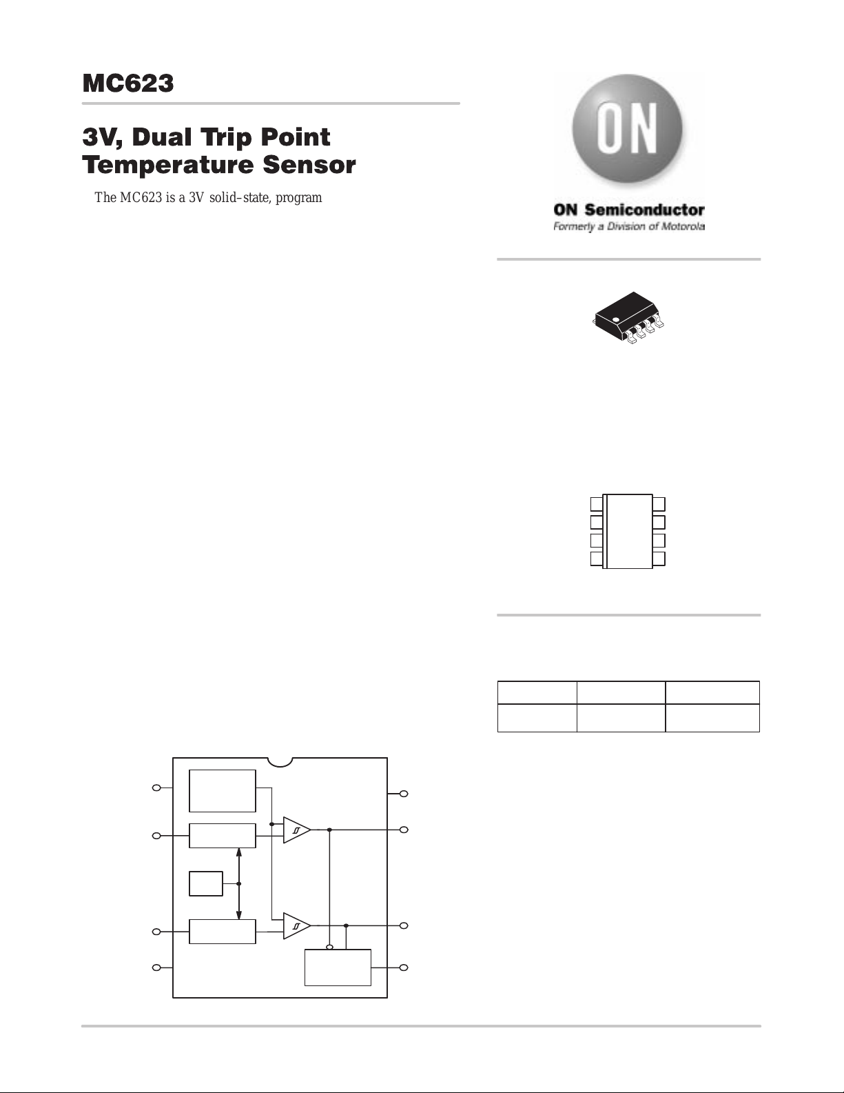
The MC623 is a 3V solid–state, programmable temperature sensor
designed for use in thermal management applications. It features dual
thermal interrupt outputs (LOW LIMIT and HIGH LIMIT) each of
which program with a single external resistor. The HIGH LIMIT and
LOW LIMIT outputs are driven active (high) when measured
temperature exceeds the user–programmed limits. The CONTROL
output is driven active (high) when temperature exceeds the HIGH
LIMIT setpoint, and turned off when temperature falls below the
LOW LIMIT setpoint. The CONTROL output can be used to provide
simple ON/OFF control to a cooling fan if so desired.
Low voltage operation, easy setpoint programming, small size and
low cost make the MC623 an ideal choice for many thermal
management applications.
Features
• Integrated T emperature Sensor and Detector Operate from a Supply
Voltage as Low as 2.7V
• Replaces Mechanical Thermostats and Switches
• On–Chip T emperature Sense
• 8–Pin SOIC for Direct PCB Mounting
• 2 User–Programmable T emperature Set Points
• 2 Independent T emperature Limit Outputs
• Heat/Cool Regulate Output
• Operating T emperature Range: –40°C to +85°C
Typical Applications
• CPU Thermal Management
• System Over–or Under–T emperature Shutdown
• Advanced Thermal Warning
• Fan Speed Control Circuits
• Accurate Appliance T emperature Sensing
• Environmental Control
http://onsemi.com
SO–8
D SUFFIX
PRELIMINARY INFORMATION
LOW SET
HIGH SET
ORDERING INFORMATION
Device Package Shipping
MC623DR2 8–Pin SOIC 2500 Tape/Reel
CASE TBD
PIN CONFIGURATION
(Top View)
V
NC
GND
1
2
MC623D
3
4
8
7
LOW LIMIT
6
HIGH LIMIT
5
CONTROL
CC
FUNCTIONAL BLOCK DIAGRAM
1
2
3
4
Temp to
Voltage
Converter
V
ref
V
ref
V
ref
R
LOW
Gen.
Gen.
< R
HIGH
NC
LOW
SET
HIGH
SET
GND
Semiconductor Components Industries, LLC, 1999
February , 2000 – Rev. 0
+
–
+
–
MC623
RS
Latch
V
CC
8
LOW
7
LIMIT
HIGH
6
LIMIT
Q
CONTROL
5
1 Publication Order Number:
MC623/D
MC623
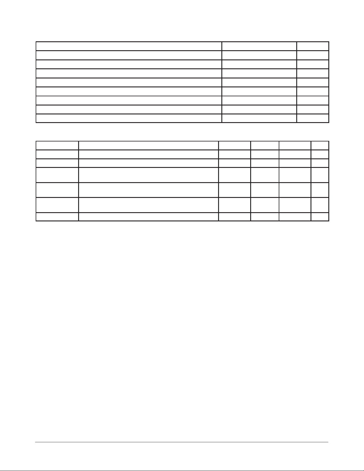
ABSOLUTE MAXIMUM RATINGS*
Parameter Value Unit
Package Power Dissipation (TA ≤ 70°C) 470 mW
Derating Factors 6.0 mW/°C
Supply Voltage 5.5 V
Input Voltage, Any Input (GND – 0.3) to (VDD + 0.3) V
Operating Temperature Range –40 to +125 °C
Maximum Chip Temperature 150 °C
Storage Temperature Range –65 to +150 °C
Lead Temperature (Soldering, 10 Seconds) +300 °C
* Maximum Ratings are those values beyond which damage to the device may occur.
ELECTRICAL CHARACTERISTICS (Over Operating Temperature Range, VDD = 2.7V to 4.5V, unless otherwise noted.)
Symbol Characteristic Min Typ
V
DD
I
DD
V
OH
V
OL
HYST Hysteresis (Falling Temperature) — — –2.0 °C
1. Measured at 25°C.
Supply Voltage Range 2.7 — 4.5 V
Supply Current (2.7V ≤ VDD ≤ 4.5V) — 150 250 µA
Absolute Accuracy
T = Programmed Temperature
IOH = 250µA
IOH = 500µA
IOL = 500µA
IOL = 1.0mA
T–3 T±1 T+3
0.9 x V
DD
0.8 x V
DD
—
—
1
—
—
—
—
Max Unit
—
—
0.1 x V
DD
0.2 x V
DD
°C
V
V
http://onsemi.com
2
 Loading...