

Motorola MC54HCT144AJ, MC74HCT144AN, MC74HCT144ASD, MC74HCT144ADT Datasheet
SEMICONDUCTOR TECHNICAL DATA
1
REV 7
Motorola, Inc. 1997
2/97
% %% ! '#%
&# #'#
'# (%
!"% "&%$
High–Performance Silicon–Gate CMOS
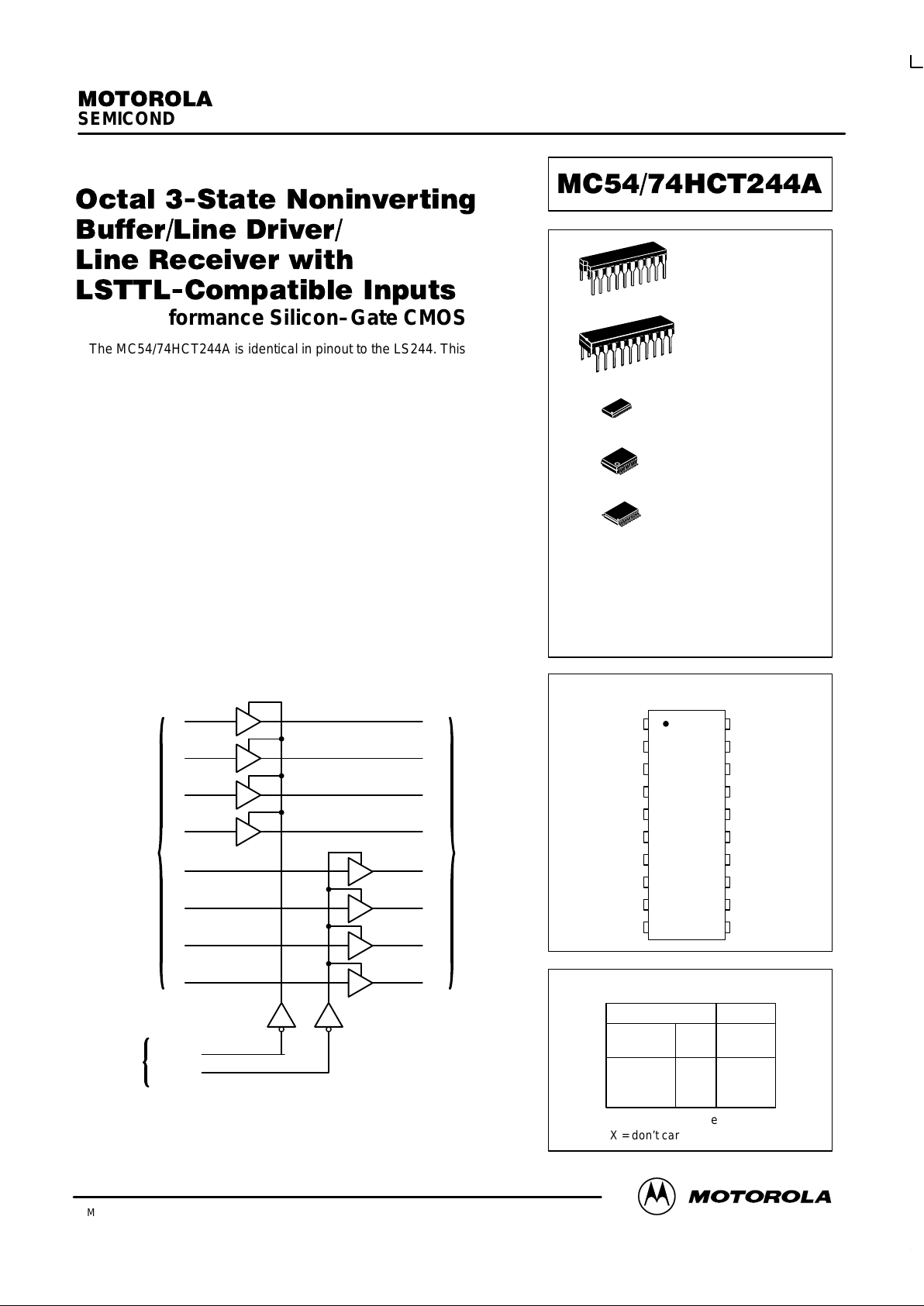
The MC54/74HCT244A is identical in pinout to the LS244. This device
may be used as a level converter for interfacing TTL or NMOS outputs to
High–Speed CMOS inputs. The HCT244A is an octal noninverting buffer
line driver line receiver designed to be used with 3–state memory address
drivers, clock drivers, and other bus–oriented systems. The device has
non–inverted outputs and two active–low output enables.
The HCT244A is the noninverting version of the HCT240. See also
HCT241.
• Output Drive Capability: 15 LSTTL Loads
• TTL NMOS–Compatible Input Levels
• Outputs Directly Interface to CMOS, NMOS, and TTL
• Operating Voltage Range: 4.5 to 5.5 V
• Low Input Current: 1 µA
• In Compliance with the Requirements Defined by JEDEC Standard
No. 7A
• Chip Complexity: 112 FETs or 28 Equivalent Gates
LOGIC DIAGRAM
DATA INPUTS
A1
A2
A3
A4
B1
B2
B3
B4
17
15
13
11
8
6
4
218
16
14
12
9
7
5
3
YB4
YB3
YB2
YB1
YA4
YA3
YA2
YA1
NONINVERTING
OUTPUTS
PIN 20 = V
CC
PIN 10 = GND
OUTPUT
ENABLES
ENABLE A
ENABLE B
1
19
PIN ASSIGNMENT
FUNCTION TABLE
Inputs Outputs
Enable A,
Enable B A, B YA, YB
LLL
LHH
HXZ
Z = high impedance
X = don’t care
A3
A2
YB4
A1
ENABLE A
GND
YB1
A4
YB2
YB3 5
4
3
2
1
10
9
8
7
6
14
15
16
17
18
19
20
11
12
13
YA2
B4
YA1
ENABLE B
V
CC
B1
YA4
B2
YA3
B3
DW SUFFIX
SOIC PACKAGE
CASE 751D–04
N SUFFIX
PLASTIC PACKAGE
CASE 738–03
ORDERING INFORMATION
MC54HCTXXXAJ
MC74HCTXXXAN
MC74HCTXXXADW
MC74HCTXXXASD
MC74HCTXXXADT
Ceramic
Plastic
SOIC
SSOP
TSSOP
DT SUFFIX
TSSOP PACKAGE
CASE 948E–02
J SUFFIX
CERAMIC PACKAGE
CASE 732–03
1
20
1
20
SD SUFFIX
SSOP PACKAGE
CASE 940C–03
1
20
1
20
1
20
MC54/74HCT244A
MOTOROLA High–Speed CMOS Logic Data
DL129 — Rev 6
2
MAXIMUM RATINGS*
Symbol
Parameter
Value
Unit
V
CC
DC Supply Voltage (Referenced to GND)
– 0.5 to + 7
V
V
in
DC Input Voltage (Referenced to GND)
– 0.5 to VCC + 0.5
V
V
out
DC Output Voltage (Referenced to GND)
– 0.5 to VCC + 0.5
V
I
in
DC Input Current, per Pin
± 20
mA
I
out
DC Output Current, per Pin
± 35
mA
I
CC
DC Supply Current, VCC and GND Pins
± 75
mA
Î
Î
Î
P
D
ОООООООООООО
Î
ОООООООООООО
Power Dissipation in Still Air,Plastic or Ceramic DIP†
SOIC Package†
SSOP or TSSOP Package†
ÎÎÎÎ
Î
ÎÎÎÎ
750
500
450
Î
Î
Î
mW
Î
T
stg
ОООООООООООО
Storage Temperature
ÎÎÎÎ
– 65 to + 150
Î
_
C
Î
Î
Î
Î
T
L
ОООООООООООО
Î
ОООООООООООО
Î
Lead Temperature, 1 mm from Case for 10 Seconds
(Plastic DIP, SOIC, SSOP or TSSOP Package)
(Ceramic DIP)
ÎÎÎÎ
Î
ÎÎÎÎ
Î
260
300
Î
Î
Î
Î
_
C
*Maximum Ratings are those values beyond which damage to the device may occur .
Functional operation should be restricted to the Recommended Operating Conditions.
†Derating — Plastic DIP: – 10 mW/_C from 65_ to 125_C
Ceramic DIP: – 10 mW/_C from 100_ to 125_C
SOIC Package: – 7 mW/_C from 65_ to 125_C
SSOP or TSSOP Package: – 6.1 mW/_C from 65_ to 125_C
For high frequency or heavy load considerations, see Chapter 2 of the Motorola High–Speed CMOS Data Book (DL129/D).
RECOMMENDED OPERATING CONDITIONS
Symbol
Parameter
Min
Max
Unit
V
CC
DC Supply Voltage (Referenced to GND)
4.5
5.5
V
Vin, V
out
DC Input Voltage, Output Voltage (Referenced to GND)
0
V
CC
V
T
A
Operating Temperature, All Package Types
– 55
+ 125
_
C
tr, t
f
Input Rise and Fall Time (Figure 1)
0
500
ns
DC ELECTRICAL CHARACTERISTICS (Voltages Referenced to GND)
Guaranteed Limit
ÎÎ
Symbol
ООООООО
Parameter
ООООООО
Test Conditions
ÎÎ
V
CC
V
ÎÎ
– 55 to
25_C
ÎÎ
v
85_C
ÎÎ
v
125_C
Î
Unit
ÎÎ
Î
V
IH
ООООООО
Î
Minimum High–Level Input
Voltage
ООООООО
Î
V
out
= 0.1 V or VCC – 0.1 V
|I
out
| v 20 µA
ÎÎ
Î
4.5
5.5
ÎÎ
2
2
ÎÎ
Î
2
2
ÎÎ
Î
2
2
Î
Î
V
ÎÎ
Î
V
IL
ООООООО
Î
Maximum Low–Level Input
Voltage
ООООООО
Î
V
out
= 0.1 V or VCC – 0.1 V
|I
out
| v 20 µA
ÎÎ
Î
4.5
5.5
ÎÎ
0.8
0.8
ÎÎ
Î
0.8
0.8
ÎÎ
Î
0.8
0.8
Î
Î
V
ÎÎ
Î
V
OH
ООООООО
Î
Minimum High–Level Output
Voltage
ООООООО
Î
Vin = VIH or V
IL
|I
out
| v 20 µA
ÎÎ
Î
4.5
5.5
ÎÎ
4.4
5.4
ÎÎ
Î
4.4
5.4
ÎÎ
Î
4.4
5.4
Î
Î
V
ÎÎÎОООООООÎООООООО
Î
Vin = VIH or V
IL
|I
out
| v 6 mA
ÎÎ
Î
4.5
ÎÎ
3.98
ÎÎ
Î
3.84
ÎÎ
Î
3.7
Î
Î
ÎÎ
Î
V
OL
ООООООО
Î
Maximum Low–Level Output
Voltage
ООООООО
Î
Vin = VIH or V
IL
|I
out
| v 20 µA
ÎÎ
Î
4.5
5.5
ÎÎ
0.1
0.1
ÎÎ
Î
0.1
0.1
ÎÎ
Î
0.1
0.1
Î
Î
V
ÎÎÎОООООООÎООООООО
Î
Vin = VIH or V
IL
|I
out
| v 6 mA
ÎÎ
Î
4.5
ÎÎ
0.26
ÎÎ
Î
0.33
ÎÎ
Î
0.4
Î
Î
I
in
Maximum Input Leakage Current
Vin = VCC or GND
5.5
± 0.1
± 1.0
± 1.0
µA
This device contains protection
circuitry to guard against damage
due to high static voltages or electric
fields. However, precautions must
be taken to avoid applications of any
voltage higher than maximum rated
voltages to this high–impedance circuit. For proper operation, Vin and
V
out
should be constrained to the
range GND v (Vin or V
out
) v VCC.
Unused inputs must always be
tied to an appropriate logic voltage
level (e.g., either GND or VCC).
Unused outputs must be left open.
MC54/74HCT244A
High–Speed CMOS Logic Data
DL129 — Rev 6
3 MOTOROLA
DC ELECTRICAL CHARACTERISTICS (Voltages Referenced to GND)
Unit
Guaranteed Limit
V
CC
V
Test Conditions
Parameter
Symbol
Unit
v
125_C
v
85_C
– 55 to
25_C
V
CC
V
Test Conditions
Parameter
Symbol
ÎÎ
Î
I
OZ
ООООООО
Î
Maximum Three–State
Leakage Current
ООООООО
Î
Output in High–Impedance State
Vin = VIL or V
IH
V
out
= VCC or GND
ÎÎ
Î
5.5
ÎÎ
± 0.5
ÎÎ
Î
± 5.0
ÎÎ
Î
± 10
Î
Î
µA
ÎÎ
Î
I
CC
ООООООО
Î
Maximum Quiescent Supply
Current (per Package)
ООООООО
Î
Vin = VCC or GND
I
out
= 0 µA
ÎÎ
Î
5.5
ÎÎ4ÎÎ
Î
40
ÎÎ
Î
160
Î
Î
µA
∆I
CC
Additional Quiescent Supply
Vin = 2.4 V, Any One Input
=
≥ –55_C
25_C to 125_C
ÎÎ
ООООООО
Current
ООООООО
V
i
n
=
V
CC
or
GND, Other Inputs
l
out
= 0 µA
ÎÎ
5.5
ÎÎÎ
2.9
ÎÎÎ
2.4
Î
mA
NOTES:
1. Information on typical parametric values along with frequency or heavy load considerations can be found in Chapter 2 of the Motorola High–
Speed CMOS Data Book (DL129/D).
2. Total Supply Current = ICC + Σ∆ICC.
AC ELECTRICAL CHARACTERISTICS (V
CC
= 5.0 V ± 10%, CL = 50 pF, Input tr = tf = 6 ns)
Guaranteed Limit
ÎÎ
Î
Symbol
ООООООООООООООООО
Î
Parameter
ÎÎ
Î
– 55 to
25_C
ÎÎ
Î
v
85_C
ÎÎ
Î
v
125_C
Î
Î
Unit
t
PLH
,
t
PHL
Maximum Propagation Delay, A to YA or B to YB
(Figures 1 and 3)
20
25
30
ns
ÎÎ
Î
t
PLZ
,
t
PHZ
ООООООООООООООООО
Î
Maximum Propagation Delay, Output Enable to YA or YB
(Figures 2 and 4)
ÎÎ
Î
26
ÎÎ
Î
33
ÎÎ
Î
39
Î
Î
ns
ÎÎ
Î
t
PZL
,
t
PZH
ООООООООООООООООО
Î
Maximum Propagation Delay, Output Enable to YA or YB
(Figures 2 and 4)
ÎÎ
Î
22
ÎÎ
Î
28
ÎÎ
Î
33
Î
Î
ns
t
TLH
,
t
THL
Maximum Output Transition Time, Any Output
(Figures 1 and 3)
12
15
18
ns
C
in
Maximum Input Capacitance
10
10
10
pF
ÎÎ
Î
C
out
ООООООООООООООООО
Î
Maximum Three–State Output Capacitance (Output in High–Impedance
State)
ÎÎ
Î
15
ÎÎ
Î
15
ÎÎ
Î
15
Î
Î
pF
NOTE:For propagation delays with loads other than 50 pF , and information on typical parametric values, see Chapter 2 of the Motorola High–
Speed CMOS Data Book (DL129/D).
Typical @ 25°C, VCC = 5.0 V
C
PD
Power Dissipation Capacitance (Per Enabled Output)*
55
pF
*Used to determine the no–load dynamic power consumption: PD = CPD V
CC
2
f + ICC VCC. For load considerations, see Chapter 2 of the
Motorola High–Speed CMOS Data Book (DL129/D).
SWITCHING W AVEFORMS
Figure 1. Figure 2.
3 V
GND
t
f
t
r
INPUT
A OR B
OUTPUT
YA OR YB
0.3 V
1.3 V
2.7 V
10%
1.3 V
90%
t
TLH
t
PLH
t
PHL
t
THL
ENABLE
A OR B
OUTPUT Y
OUTPUT Y
1.3 V
1.3 V
1.3 V
90%
10%
t
PZL
t
PLZ
t
PZHtPHZ
3 V
GND
HIGH
IMPEDANCE
V
OL
V
OH
HIGH
IMPEDANCE
 Loading...