

Motorola MC54HC646J, MC74HC646DW, MC74HC646N Datasheet
SEMICONDUCTOR TECHNICAL DATA
3–1
REV 6
Motorola, Inc. 1995
10/95
! "
High–Performance Silicon–Gate CMOS
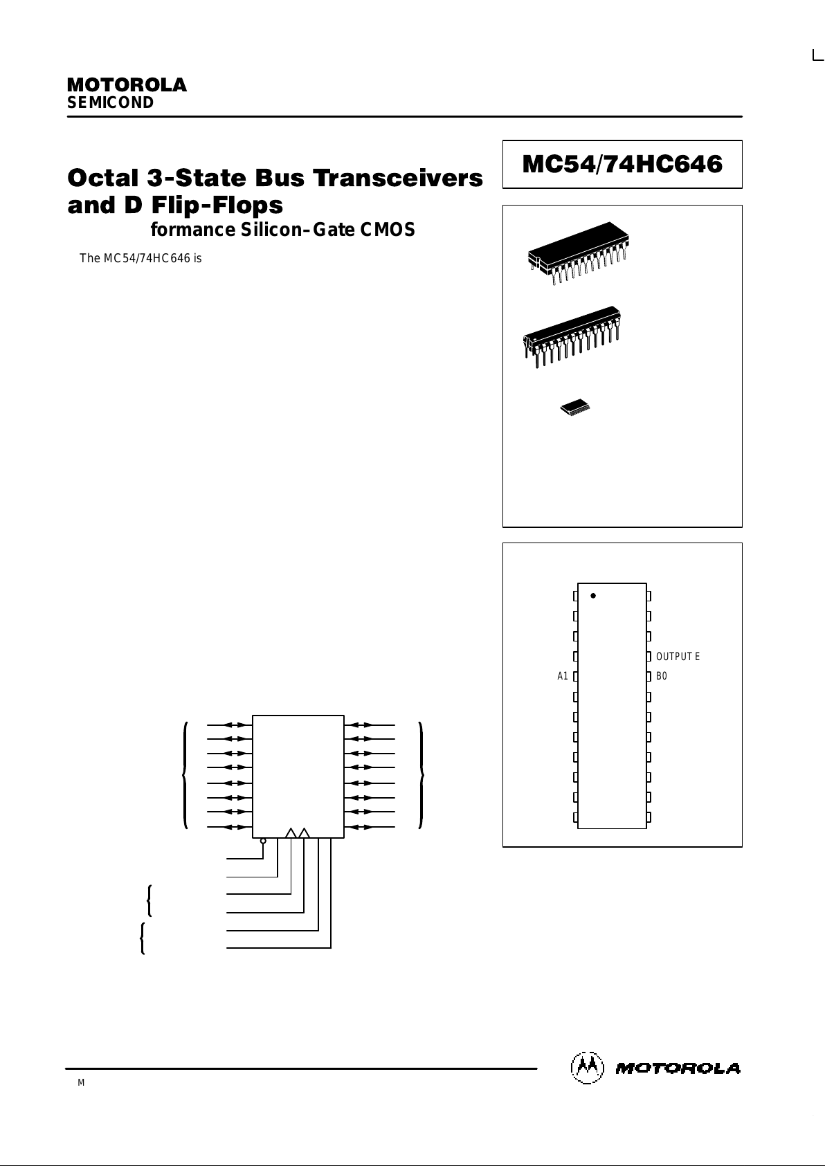
The MC54/74HC646 is identical in pinout to the LS646. The device inputs
are compatible with standard CMOS outputs; with pullup resistors, they are
compatible with LSTTL outputs.
These devices are bus transceivers with D flip–flops. Depending on the
status of the Data–Source Selection pins, data may be routed to the outputs
either from the flip–flops or transmitted real–time from the inputs (see
Function Table and Application Information).
The Output Enable and t he Direction pins control the transceiver’s
function. Bus A and Bus B cannot be routed as outputs to e ach other
simultaneously, but can be routed as inputs to the A and B flip–flops. Also,
the A and B flip–flops can be routed a s outputs to Bus A a nd Bus B.
Additionally, when either or both of the ports are in the high–impedance
state, these I/O pins may be used as inputs to t he D flip–flops for data
storage.
The user should note that because the clocks are not gated with the
Direction and Output Enable pins, data at the A and B ports may be clocked
into the storage flip–flops at any time.
• Output Drive Capability: 15 LSTTL Loads
• Outputs Directly Interface to CMOS, NMOS, and TTL
• Operating Voltage Range: 2 to 6 V
• Low Input Current: 1 µA
• High Noise Immunity Characteristic of CMOS Devices
• In Compliance with the Requirements Defined by JEDEC Standard
No. 7A
• Chip Complexity: 780 FETs or 195 Equivalent Gates
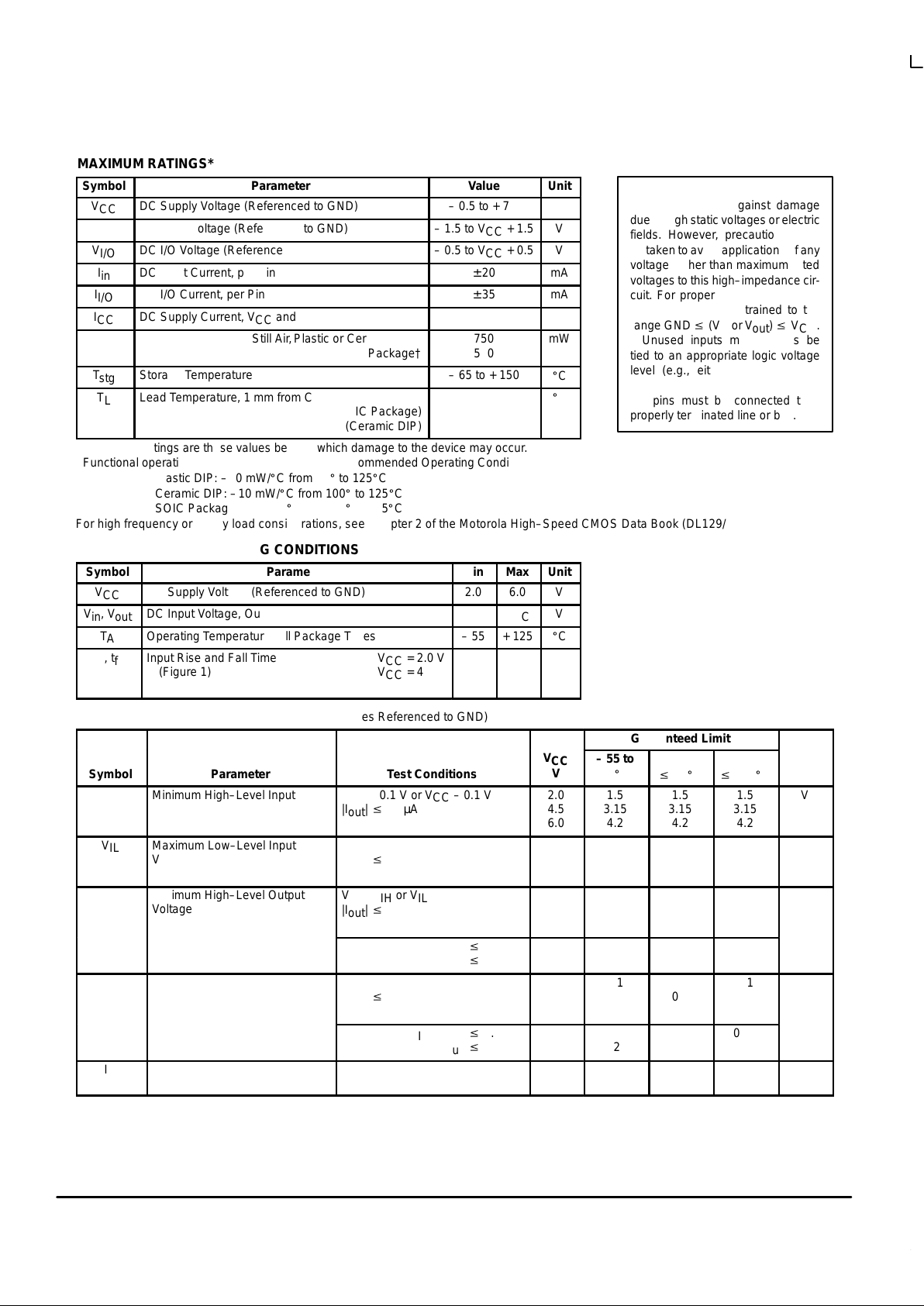
LOGIC DIAGRAM
A
DATA
PORT
B
DATA
PORT
A0
A1
A2
A3
A4
A5
A6
A7
11
10
9
8
7
6
5
4 20
B0
19
18
17
16
15
14
13
B1
B2
B3
B4
B5
B6
B7
21
3
1
23
2
22
A–TO–B SOURCE
B–TO–A SOURCE
B–TO–A CLOCK
A–TO–B CLOCK
DIRECTION
OUTPUT ENABLE
FLIP–FLOP
CLOCKS
DATA SOURCE
SELECTION
INPUTS
PIN 24 = V
CC
PIN 12 = GND
PIN ASSIGNMENT
A2
A0
DIRECTION
A–TO–B
SOURCE
A–TO–B
CLOCK
A4
A3
A1 B0
OUTPUT ENABLE
B–TO–A
SOURCE
B–TO–A
CLOCK
V
CC
B5
B4
B3
5
4
3
2
1
10
9
8
7
6
14
15
16
17
18
19
20
13
11
12
21
22
23
24
B7
B6
B2
B1
A7
GND
A6
A5
N SUFFIX
PLASTIC PACKAGE
CASE 724–03
ORDERING INFORMATION
MC54HCXXXJ
MC74HCXXXN
MC74HCXXXDW
Ceramic
Plastic
SOIC
1
24
J SUFFIX
CERAMIC PACKAGE
CASE 758–02
DW SUFFIX
SOIC PACKAGE
CASE 751E–04
1
24
1
24
MC54/74HC646
MOTOROLA High–Speed CMOS Logic Data
DL129 — Rev 6
3–2
MAXIMUM RATINGS*
Symbol
Parameter
Value
Unit
V
CC
DC Supply Voltage (Referenced to GND)
– 0.5 to + 7.0
V
V
in
DC Input Voltage (Referenced to GND)
– 1.5 to VCC + 1.5
V
V
I/O
DC I/O Voltage (Referenced to GND)
– 0.5 to VCC + 0.5
V
I
in
DC Input Current, per Pin
± 20
mA
I
I/O
DC I/O Current, per Pin
± 35
mA
I
CC
DC Supply Current, VCC and GND Pins
± 75
mA
P
D
Power Dissipation in Still Air,Plastic or Ceramic DIP†
SOIC Package†
750
500
mW
T
stg
Storage Temperature
– 65 to + 150
_
C
T
L
Lead Temperature, 1 mm from Case for 10 Seconds
(Plastic DIP or SOIC Package)
(Ceramic DIP)
260
300
_
C
*Maximum Ratings are those values beyond which damage to the device may occur.
Functional operation should be restricted to the Recommended Operating Conditions.
†Derating — Plastic DIP: –10 mW/_C from 65_ to 125_C
Ceramic DIP: –10 mW/_C from 100_ to 125_C
SOIC Package: – 7 mW/_C from 65_ to 125_C
For high frequency or heavy load considerations, see Chapter 2 of the Motorola High–Speed CMOS Data Book (DL129/D).
RECOMMENDED OPERATING CONDITIONS
Symbol
Parameter
Min
Max
Unit
V
CC
DC Supply Voltage (Referenced to GND)
2.0
6.0
V
Vin, V
out
DC Input Voltage, Output Voltage (Referenced to GND)
0
V
CC
V
T
A
Operating Temperature, All Package Types
– 55
+ 125
_
C
tr, t
f
Input Rise and Fall Time VCC = 2.0 V
(Figure 1) VCC = 4.5 V
VCC = 6.0 V
0
0
0
1000
500
400
ns
DC ELECTRICAL CHARACTERISTICS (Voltages Referenced to GND)
Guaranteed Limit
Symbol
Parameter
Test Conditions
V
CC
V
– 55 to
25_C
v
85_Cv 125_C
Unit
V
IH
Minimum High–Level Input
Voltage
V
out
= 0.1 V or VCC – 0.1 V
|I
out
| v 20 µA
2.0
4.5
6.0
1.5
3.15
4.2
1.5
3.15
4.2
1.5
3.15
4.2
V
V
IL
Maximum Low–Level Input
Voltage
V
out
= 0.1 V or VCC – 0.1 V
|I
out
| v 20 µA
2.0
4.5
6.0
0.3
0.9
1.2
0.3
0.9
1.2
0.3
0.9
1.2
V
V
OH
Minimum High–Level Output
Voltage
Vin = VIH or V
IL
|I
out
| v 20 µA
2.0
4.5
6.0
1.9
4.4
5.9
1.9
4.4
5.9
1.9
4.4
5.9
V
Vin = VIH or VIL|I
out
| v 6.0 mA
|I
out
| v 7.8 mA
4.5
6.0
3.98
5.48
3.84
5.34
3.70
5.20
V
OL
Maximum Low–Level Output
Voltage
Vin = VIH or V
IL
|I
out
| v 20 µA
2.0
4.5
6.0
0.1
0.1
0.1
0.1
0.1
0.1
0.1
0.1
0.1
V
Vin = VIH or VIL|I
out
| v 6.0 mA
|I
out
| v 7.8 mA
4.5
6.0
0.26
0.26
0.33
0.33
0.40
0.40
I
in
Maximum Input Leakage Current
Vin = VCC or GND
(Pins 1, 2, 3, 21, 22, and 23)
6.0
± 0.1
± 1.0
± 1.0
µA
This device contains protection
circuitry to guard against damage
due to high static voltages or electric
fields. However, precautions must
be taken to avoid applications of any
voltage higher than maximum rated
voltages to this high–impedance circuit. For proper operation, Vin and
V
out
should be constrained to the
range GND v (Vin or V
out
) v VCC.
Unused inputs must always be
tied to an appropriate logic voltage
level (e.g., either GND or VCC).
Unused outputs must be left open.
I/O pins must be connected to a
properly terminated line or bus.
MC54/74HC646
High–Speed CMOS Logic Data
DL129 — Rev 6
3–3 MOTOROLA
DC ELECTRICAL CHARACTERISTICS (Voltages Referenced to GND)
Unit
v
125_C
v
85_C
– 55 to
25_C
V
CC
V
Test Conditions
Parameter
Symbol
I
OZ
Maximum Three–State Leakage
Current
Output in High–Impedance State
Vin = VIL or V
IH
V
out = VCC
or GND, I/O Pins
6.0
± 0.5
± 5.0
± 10
µA
I
CC
Maximum Quiescent Supply
Current (per Package)
Vin = VCC or GND
I
out
= 0 µA
6.0
8
80
160
µA
NOTE: Information on typical parametric values can be found in Chapter 2 of the Motorola High–Speed CMOS Data Book (DL129/D).
MC54/74HC646
MOTOROLA High–Speed CMOS Logic Data
DL129 — Rev 6
3–4
AC ELECTRICAL CHARACTERISTICS (C
L
= 50 pF, Input tr = tf = 6 ns)
Guaranteed Limit
Symbol
Parameter
V
CC
V
– 55 to
25_C
v
85_Cv 125_C
Unit
f
max
Maximum Clock Frequency (50% Duty Cycle)
(Figures 3, 4 and 9)
2.0
4.5
6.0
6.0
30
35
4.8
24
28
4.0
20
24
MHz
t
PLH
,
t
PHL
Maximum Propagation Delay, Input A to Output B
(or Input B to Output A)
(Figures 1, 2 and 9)
2.0
4.5
6.0
170
34
29
215
43
37
255
51
43
ns
t
PLH
,
t
PHL
Maximum Propagation Delay, A–to–B Clock to Output B
(or B–to–A Clock to Output A)
(Figures 3, 4 and 9)
2.0
4.5
6.0
220
44
37
275
55
47
330
66
56
ns
t
PLH
,
t
PHL
Maximum Propagation Delay, A–to–B Source to Output B
(or B–to–A Source to Output A)
(Figures 5, 6 and 9)
2.0
4.5
6.0
170
34
29
215
43
37
255
51
43
ns
t
PLZ
,
t
PHZ
Maximum Propagation Delay, Output Enable to Output A or B
(Figures 7, 8 and 10)
2.0
4.5
6.0
175
35
30
220
44
37
265
53
45
ns
t
PZL
,
t
PZH
Maximum Propagation Delay, Direction or Output Enable to
Output A or B
(Figures 7, 8 and 10)
2.0
4.5
6.0
175
35
30
220
44
37
265
53
45
ns
t
TLH
,
t
THL
Maximum Output Transition Time, Any Output
(Figures 1 and 9)
2.0
4.5
6.0
60
12
10
75
15
13
90
18
15
ns
C
in
Maximum Input Capacitance
—
10
10
10
pF
C
out
Maximum Three–State Output Capacitance
(Output in High–Impedance State)
—
15
15
15
pF
NOTES:
1. For propagation delays with loads other than 50 pF, see Chapter 2 of the Motorola High–Speed CMOS Data Book (DL129/D).
2. Information on typical parametric values can be found in Chapter 2 of the Motorola High–Speed CMOS Data Book (DL129/D).
Typical @ 25°C, VCC = 5.0 V
C
PD
Power Dissipation Capacitance (Per Channel)*
60
pF
*Used to determine the no–load dynamic power consumption: PD = CPD V
CC
2
f + ICC VCC. For load considerations, see Chapter 2 of the
Motorola High–Speed CMOS Data Book (DL129/D).
TIMING REQUIREMENTS (Input t
r
= tf = 6 ns)
Guaranteed Limit
Symbol
Parameter
V
CC
V
– 55 to
25_C
v
85_Cv 125_C
Unit
t
su
Minimum Setup Time, Input A to A–to–B Clock
(or Input B to B–to–A Clock)
(Figures 3 and 4)
2.0
4.5
6.0
100
20
17
125
25
21
150
30
26
ns
t
h
Minimum Hold Time, A–to–B Clock to Input A
(or B–to–A Clock to Input B)
(Figures 3 and 4)
2.0
4.5
6.0
5
5
5
5
5
5
5
5
5
ns
t
w
Minimum Pulse Width, A–to–B Clock (or B–to–A Clock)
(Figures 3 and 4)
2.0
4.5
6.0
80
16
14
100
20
17
120
24
20
ns
tr, t
f
Maximum Input Rise and Fall Times
(Figure 1)
2.0
4.5
6.0
1000
500
400
1000
500
400
1000
500
400
ns
NOTE: Information on typical parametric values can be found in Chapter 2 of the Motorola High–Speed CMOS Data Book (DL129/D).
MC54/74HC646
High–Speed CMOS Logic Data
DL129 — Rev 6
3–5 MOTOROLA
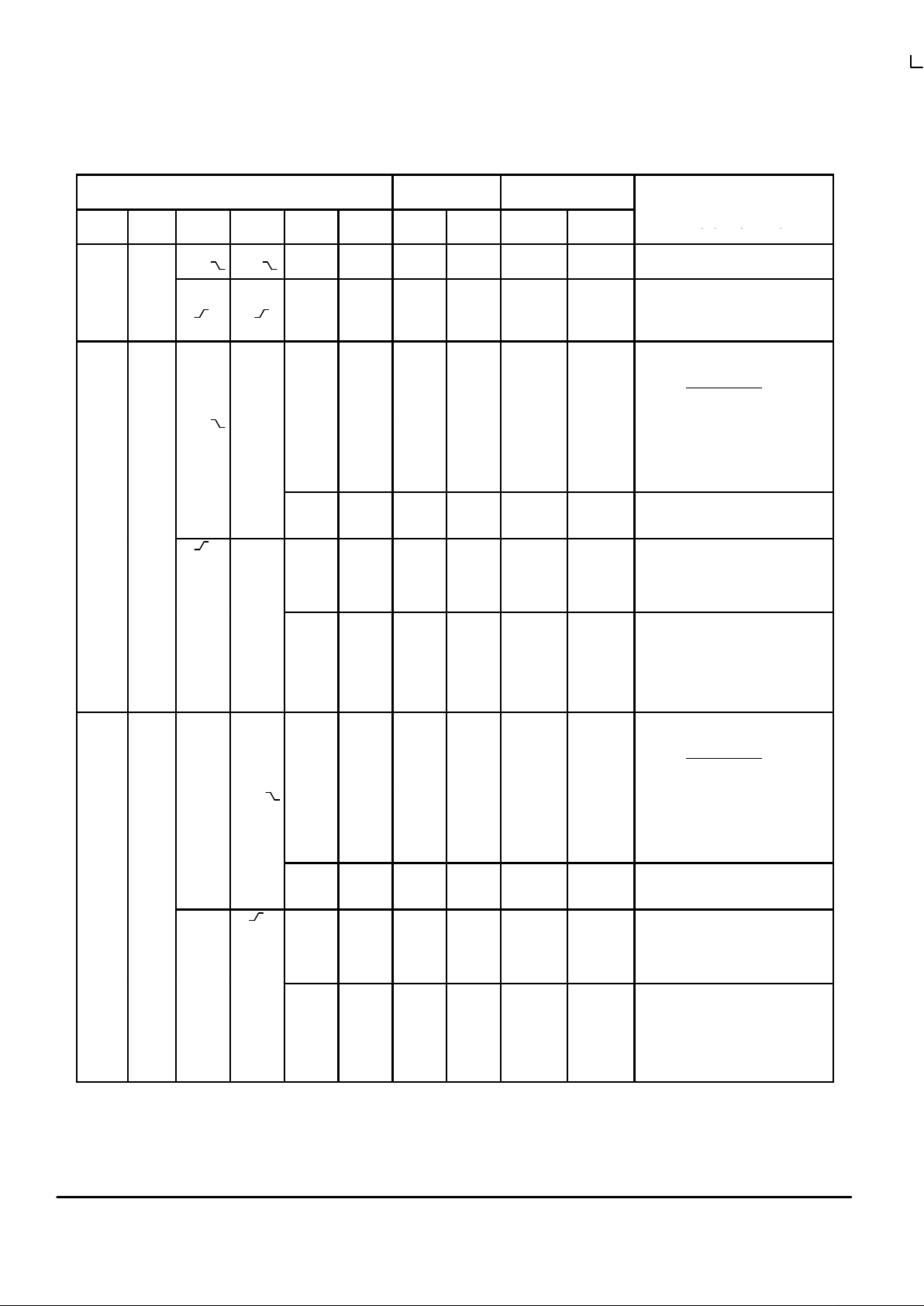
FUNCTION TABLE — HC646
Control Inputs Data Port Status
Storage Flip–
Flop States
Output
Enable
Direc–
tion
A–to–B
Clock
B–to–A
Clock
A–to–B
Source
B–to–A
Source
A B Q
A
Q
B
Description of Operation
H X
H, L, H, L, X X
Input:XInput:
X
no change no change
The output functions of the A and B
ports are disabled
X X
L
H
X
X
X
X
L
H
L
H
X
X
X
X
L
H
The ports may be used as inputs to
the storage flip–flops. Data at the inputs are clocked into the flip–flops
with the rising edge of the Clocks.
L H
Input: Output:
The output mode of the B data port is
enabled and behaves according to
the following logic equation:
B = [A • (A–to–B Source
)]
+ [Q
A
• (A–to–B Source)]
H, L, X* L X L
H
L
H
no change
no change
no change
no change
1.) When A–to–B Source is low, the
data at the A data port are displayed at the B data port. The
states of the storage flip–flops are
not affected.
H X X Q
A
no change no change 2.) When A–to–B Source is high, the
states of the A storage flip–flops are
displayed at the B data port.
X* L X L
H
L
H
L
H
no change
no change
3.) When A–to–B Source is low, the
data at the A data port are clocked
into the A storage flip–flops by a rising–edge signal on the A–to–B
Clock.
H X L
H
Q
A
Q
A
L
H
no change
no change
4.) When A–to–B Source is high, the
data at the A data port are clocked
into the A storage flip–flops by a rising–edge signal on the A–to–B
Clock. The states, QA, of the storage flip–flops propagate directly to
the B data port.
L L
Output: Input:
The output mode of the A data port is
enabled and behaves according to
the following logic equation:
A = [B • (B–to–A Source
)]
+ [Q
B
• (B–to–A Source)]
X* H, L, X L L
H
L
H
no change
no change
no change
no change
1.) When B–to–A Source is low, the
data at the B data port are displayed at the A data port. The
states of the storage flip–flops are
not affected.
X H Q
B
X no change no change 2.) When B–to–A Source is high, the
states of the B storage flip–flops are
displayed at the A data port.
X* X L L
H
L
H
no change
no change
L
H
3.) When B–to–A Source is low, the
data at the B data port are clocked
into the B storage flip–flops by a rising–edge signal on the B–to–A
Clock.
X H Q
B
Q
B
L
H
no change
no change
L
H
4.) When B–to–A Source is high, the
data at the B data port are clocked
into the B storage flip–flops by a rising–edge signal on the B–to–A
Clock. The states, QB, of the storage flip–flops propagate directly to
the A data port.
*The clocks are not internally gated with either the Output Enables or the Source inputs. Therefore, data at the A and B ports may be clocked into
the storage flip–flops at any time.
 Loading...