

Motorola MC54HC597J, MC74HC597N Datasheet
SEMICONDUCTOR TECHNICAL DATA
1
REV 6
Motorola, Inc. 1995
10/95
" #"
#"#" " !"
$" #" "
High–Performance Silicon–Gate CMOS
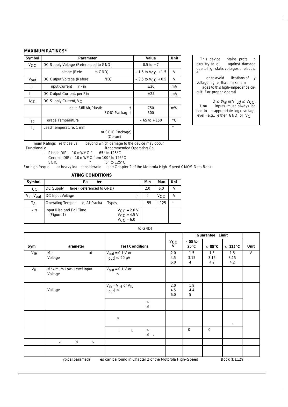
The MC54/74HC597 is identical in pinout to the LS597. The device inputs
are compatible with standard CMOS outputs; with pullup resistors, they are
compatible with LSTTL outputs.
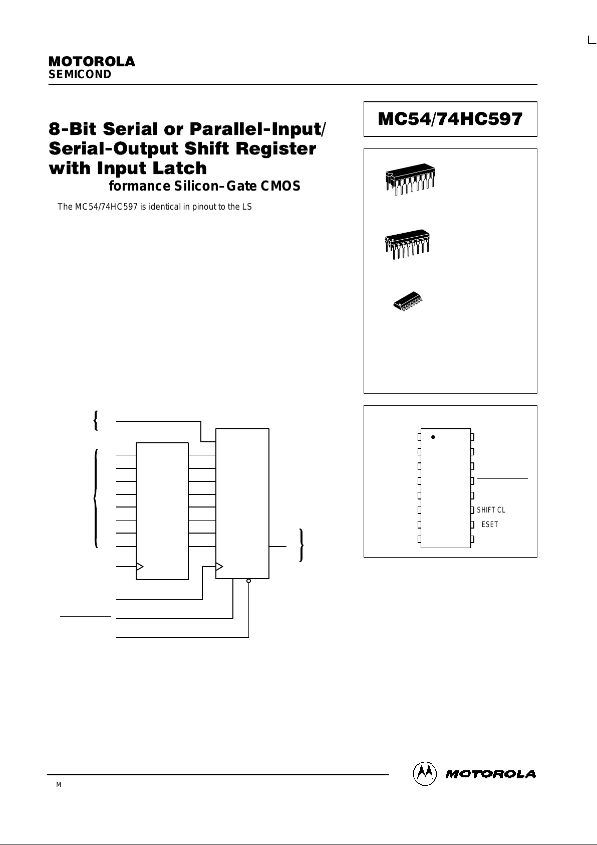
This device consists of an 8–bit input latch which feeds parallel data to an
8–bit shift register. Data can also be loaded serially (see Function Table).
The HC597 is similar in function to the HC589, which is a 3–state device.
• Output Drive Capability: 10 LSTTL Loads
• Outputs Directly Interface to CMOS, NMOS, and TTL
• Operating Voltage Range: 2 to 6 V
• Low Input Current: 1 µA
• High Noise Immunity Characteristic of CMOS Devices
• In Compliance with the Requirements Defined by JEDEC Standard
No. 7A
• Chip Complexity: 516 FETs or 129 Equivalent Gates
LOGIC DIAGRAM
SERIAL
DATA
INPUT
14
15
1
2
3
4
5
6
7
12
11
13
10
S
A
A
B
C
D
E
F
G
H
LATCH CLOCK
SHIFT CLOCK
SERIAL SHIFT/
PARALLEL LOAD
RESET
PARALLEL
DATA
INPUTS
INPUT
LATCH
SHIFT
REGISTER
PIN 16 = V
CC
PIN 8 = GND
9
Q
H
SERIAL
DATA
OUTPUT
PIN ASSIGNMENT
13
14
15
16
9
10
11
125
4
3
2
1
8
7
6
LATCH CLOCK
SERIAL SHIFT/
PARALLEL LOAD
S
A
A
V
CC
Q
H
RESET
SHIFT CLOCK
E
D
C
B
GND
H
G
F
D SUFFIX
SOIC PACKAGE
CASE 751B–05
N SUFFIX
PLASTIC PACKAGE
CASE 648–08
ORDERING INFORMATION
MC54HCXXXJ
MC74HCXXXN
MC74HCXXXD
Ceramic
Plastic
SOIC
1
16
1
16
J SUFFIX
CERAMIC PACKAGE
CASE 620–10
1
16
MC54/74HC597
MOTOROLA High–Speed CMOS Logic Data
DL129 — Rev 6
2
MAXIMUM RATINGS*
Symbol
Parameter
Value
Unit
V
CC
DC Supply Voltage (Referenced to GND)
– 0.5 to + 7.0
V
V
in
DC Input Voltage (Referenced to GND)
– 1.5 to VCC + 1.5
V
V
out
DC Output Voltage (Referenced to GND)
– 0.5 to VCC + 0.5
V
I
in
DC Input Current, per Pin
± 20
mA
I
out
DC Output Current, per Pin
± 25
mA
I
CC
DC Supply Current, VCC and GND Pins
± 50
mA
P
D
Power Dissipation in Still Air,Plastic or Ceramic DIP†
SOIC Package†
750
500
mW
T
stg
Storage Temperature
– 65 to + 150
_
C
T
L
Lead Temperature, 1 mm from Case for 10 Seconds
(Plastic DIP or SOIC Package)
(Ceramic DIP)
260
300
_
C
*Maximum Ratings are those values beyond which damage to the device may occur.
Functional operation should be restricted to the Recommended Operating Conditions.
†Derating — Plastic DIP: – 10 mW/_C from 65_ to 125_C
— Ceramic DIP: – 10 mW/_C from 100_ to 125_C
— SOIC Package: – 7 mW/_C from 65_ to 125_C
For high frequency or heavy load considerations, see Chapter 2 of the Motorola High–Speed CMOS Data Book (DL129/D).
RECOMMENDED OPERATING CONDITIONS
Symbol
Parameter
Min
Max
Unit
V
CC
DC Supply Voltage (Referenced to GND)
2.0
6.0
V
Vin, V
out
DC Input Voltage, Output Voltage (Referenced to GND)
0
V
CC
V
T
A
Operating Temperature, All Package Types
– 55
+ 125
_
C
tr, t
f
Input Rise and Fall Time VCC = 2.0 V
(Figure 1) VCC = 4.5 V
VCC = 6.0 V
0
0
0
1000
500
400
ns
DC ELECTRICAL CHARACTERISTICS (Voltages Referenced to GND)
Guaranteed Limit
Symbol
Parameter
Test Conditions
V
CC
V
– 55 to
25_C
v
85_Cv 125_C
Unit
V
IH
Minimum High–Level Input
Voltage
V
out
= 0.1 V or VCC – 0.1 V
|I
out
| v 20 µA
2.0
4.5
6.0
1.5
3.15
4.2
1.5
3.15
4.2
1.5
3.15
4.2
V
V
IL
Maximum Low–Level Input
Voltage
V
out
= 0.1 V or VCC – 0.1 V
|I
out
| v 20 µA
2.0
4.5
6.0
0.3
0.9
1.2
0.3
0.9
1.2
0.3
0.9
1.2
V
V
OH
Minimum High–Level Output
Voltage
Vin = VIH or V
IL
|I
out
| v 20 µA
2.0
4.5
6.0
1.9
4.4
5.9
1.9
4 4
5.9
1.9
4 4
5.9
V
Vin = VIH or VIL|I
out
| v 4.0 mA
|I
out
| v 5.2 mA
4.5
6.0
3.98
5.48
3.84
5.34
3.70
5.20
V
OL
Maximum Low–Level Output
Voltage
Vin = VIH or V
IL
|I
out
| v 20 µA
2.0
4.5
6.0
0.1
0.1
0.1
0.1
0.1
0.1
0.1
0.1
0.1
V
Vin = VIH or VIL|I
out
| v 4.0 mA
|I
out
| v 5.2 mA
4.5
6.0
0.26
0.26
0.33
0.33
0.40
0.40
I
in
Maximum Input Leakage Current
Vin = VCC or GND
6.0
± 0.1
± 1.0
± 1.0
µA
I
CC
Maximum Quiescent Supply
Current (per Package)
Vin = VCC or GND
I
out
= 0 µA
6.0
8
80
160
µA
NOTE: Information on typical parametric values can be found in Chapter 2 of the Motorola High–Speed CMOS Data Book (DL129/D).
This device contains protection
circuitry to guard against damage
due to high static voltages or electric
fields. However, precautions must
be taken to avoid applications of any
voltage higher than maximum rated
voltages to this high–impedance circuit. For proper operation, Vin and
V
out
should be constrained to the
range GND v (Vin or V
out
) v VCC.
Unused inputs must always be
tied to an appropriate logic voltage
level (e.g., either GND or VCC).
Unused outputs must be left open.
MC54/74HC597
High–Speed CMOS Logic Data
DL129 — Rev 6
3 MOTOROLA
AC ELECTRICAL CHARACTERISTICS (C
L
= 50 pF, Input tr = tf = 6 ns)
Guaranteed Limit
Symbol
Parameter
V
CC
V
– 55 to
25_C
v
85_Cv 125_C
Unit
f
max
Maximum Clock Frequency (50% Duty Cycle)
(Figures 2 and 8)
2.0
4.5
6.0
6.0
30
35
4.8
24
28
4.0
20
24
MHz
t
PLH
,
t
PHL
Maximum Propagation Delay, Latch Clock to Q
H
(Figures 1 and 8)
2.0
4.5
6.0
210
42
36
265
53
45
315
63
54
ns
t
PLH
,
t
PHL
Maximum Propagation Delay, Shift Clock to Q
H
(Figures 2 and 8)
2.0
4.5
6.0
175
35
30
220
44
37
265
53
45
ns
t
PHL
Maximum Propagation Delay, Reset to Q
H
(Figures 3 and 8)
2.0
4.5
6.0
175
35
30
220
44
37
265
53
45
ns
t
PLH
,
t
PHL
Maximum Propagation Delay, Serial Shift/Parallel Load to Q
H
(Figures 4 and 8)
2.0
4.5
6.0
175
35
30
220
44
37
265
53
45
ns
t
TLH
,
t
THL
Maximum Output Transition Time, Any Output
(Figures 1 and 8)
2.0
4.5
6.0
75
15
13
95
19
16
110
22
19
ns
C
in
Maximum Input Capacitance
—
10
10
10
pF
NOTES:
1. For propagation delays with loads other than 50 pF, see Chapter 2 of the Motorola High–Speed CMOS Data Book (DL129/D).
2. Information on typical parametric values can be found in Chapter 2 of the Motorola High–Speed CMOS Data Book (DL129/D).
Typical @ 25°C, VCC = 5.0 V
C
PD
Power Dissipation Capacitance (Per Package)*
50
pF
*Used to determine the no–load dynamic power consumption: PD = CPD V
CC
2
f + ICC VCC. For load considerations, see Chapter 2 of the
Motorola High–Speed CMOS Data Book (DL129/D).
PIN DESCRIPTIONS
DATA INPUTS
A, B, C, D, E, F, G, H (Pins 15, 1, 2, 3, 4, 5, 6, 7)
Parallel data inputs. Data on these inputs is stored in the
input latch on the rising edge of the Latch Clock input.
SA (Pin 14)
Serial data input. Data on this input is shifted into the shift
register on the rising edge of the Shift Clock input it Serial
Shift/Parallel Load
is high. Data on this input is ignored when
Serial Shift/Parallel Load
is low.
CONTROL INPUTS
Serial Shift/Parallel Load
(Pin 13)
Shift register mode control. When a high level is applied to
this pin, the shift register is allowed to serially shift data.
When a low level is applied to this pin, the shift register
accepts parallel data from the input latch, and serial shifting
is inhibited.
Reset (Pin 10)
Asynchronous, Active–low shift register reset. A low level
applied to this input resets the shift register to a low level, but
does not change the data in the input latch.
Shift Clock (Pin 11)
Serial shift register clock. A low–to–high transition on this
input shifts data on the Serial Data Input into the shift register
and data in stage H is shifted out QH, being replaced by the
data previously stored in stage G.
Latch Clock (Pin 12)
Latch clock. A low–to–high transition on this input loads
the parallel data on inputs A–H into the input latch.
OUTPUT
QH (Pin 9)
Serial data output. This pin is the output from the last stage
of the shift register.
 Loading...