

Motorola MC54HC589AJ, MC74HC589AN, MC74HC589AD, MC74HC589ADT Datasheet
SEMICONDUCTOR TECHNICAL DATA
1
REV 0
Motorola, Inc. 1995
10/95
" #"
#"#" " !"
$" "" #"#"
High–Performance Silicon–Gate CMOS
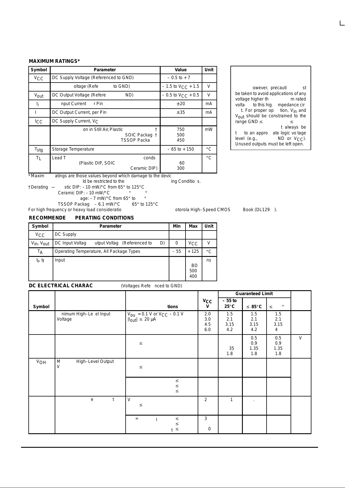
The MC54/74HC589A is similar in function to the HC597, which is not a
3–state device. The device i nputs are compatible with standard CMOS
outputs, with pullup resistors, they are compatible with LSTTL outputs.
This device consists of an 8–bit storage latch which feeds parallel data to
an 8–bit shift register. Data can also be loaded serially (see Function Table).
The shift register output, QH, is a three–state output, allowing this device to
be used in bus–oriented systems.
The HC589A directly interfaces with the Motorola SPI serial data port on
CMOS MPUs and MCUs.
• Output Drive Capability: 15 LSTTL Loads
• Outputs Directly Interface to CMOS, NMOS, and TTL
• Operating Voltage Range: 2 to 6 V
• Low Input Current: 1 µA
• High Noise Immunity Characteristic of CMOS Devices
• In Compliance with the Requirements Defined by JEDEC Standard
No. 7A
• Chip Complexity: 526 FETs or 131.5 Equivalent Gates
LOGIC DIAGRAM
SERIAL
DATA
INPUT
14
15
1
2
3
4
5
6
7
12
11
13
10
S
A
A
B
C
D
E
F
G
H
LATCH CLOCK
SHIFT CLOCK
SERIAL SHIFT/
PARALLEL LOAD
OUTPUT ENABLE
PARALLEL
DATA
INPUTS
DATA
LATCH
SHIFT
REGISTER
VCC = PIN 16
GND = PIN 8
9
Q
H
SERIAL
DATA
OUTPUT
This document contains information on a product under development. Motorola reserves the right to change or discontinue this product without notice.
PIN ASSIGNMENT
13
14
15
16
9
10
11
125
4
3
2
1
8
7
6
LATCH CLOCK
SERIAL SHIFT/
PARALLEL LOAD
S
A
A
V
CC
Q
H
OUTPUT ENABLE
SHIFT CLOCK
E
D
C
B
GND
H
G
F
D SUFFIX
SOIC PACKAGE
CASE 751B–05
N SUFFIX
PLASTIC PACKAGE
CASE 648–08
ORDERING INFORMATION
MC54HCXXXAJ
MC74HCXXXAN
MC74HCXXXAD
MC74HCXXXADT
Ceramic
Plastic
SOIC
TSSOP
1
16
1
16
J SUFFIX
CERAMIC PACKAGE
CASE 620–10
1
16
1
16
DT SUFFIX
TSSOP PACKAGE
CASE 948F–01
MC54/74HC589A
MOTOROLA High–Speed CMOS Logic Data
DL129 — Rev 6
2
MAXIMUM RATINGS*
Symbol
Parameter
Value
Unit
V
CC
DC Supply Voltage (Referenced to GND)
– 0.5 to + 7.0
V
V
in
DC Input Voltage (Referenced to GND)
– 1.5 to VCC + 1.5
V
V
out
DC Output Voltage (Referenced to GND)
– 0.5 to VCC + 0.5
V
I
in
DC Input Current, per Pin
± 20
mA
I
out
DC Output Current, per Pin
± 35
mA
I
CC
DC Supply Current, VCC and GND Pins
± 75
mA
P
D
Power Dissipation in Still Air,Plastic or Ceramic DIP†
SOIC Package†
TSSOP Package†
750
500
450
mW
T
stg
Storage Temperature
– 65 to + 150
_
C
T
L
Lead Temperature, 1 mm from Case for 10 Seconds
(Plastic DIP, SOIC or TSSOP Package)
(Ceramic DIP)
260
300
_
C
*Maximum Ratings are those values beyond which damage to the device may occur.
Functional operation should be restricted to the Recommended Operating Conditions.
†Derating — Plastic DIP: –10 mW/_C from 65_ to 125_C
Ceramic DIP: –10 mW/_C from 100_ to 125_C
SOIC Package: –7 mW/_C from 65_ to 125_C
TSSOP Package: – 6.1 mW/_C from 65_ to 125_C
For high frequency or heavy load considerations, see Chapter 2 of the Motorola High–Speed CMOS Data Book (DL129/D).
RECOMMENDED OPERATING CONDITIONS
Symbol
Parameter
Min
Max
Unit
V
CC
DC Supply Voltage (Referenced to GND)
2.0
6.0
V
Vin, V
out
DC Input Voltage, Output Voltage (Referenced to GND)
0
V
CC
V
T
A
Operating Temperature, All Package Types
– 55
+ 125
_
C
tr, t
f
Input Rise and Fall Time VCC = 2.0 V
VCC = 3.0 V
(Figure 1) VCC = 4.5 V
VCC = 6.0 V
0
0
0
1000
TBD
500
400
ns
DC ELECTRICAL CHARACTERISTICS (Voltages Referenced to GND)
Guaranteed Limit
Symbol
Parameter
Test Conditions
V
CC
V
– 55 to
25_C
v
85_Cv 125_C
Unit
V
IH
Minimum High–Level Input
Voltage
V
out
= 0.1 V or VCC – 0.1 V
|I
out
| v 20 µA
2.0
3.0
4.5
6.0
1.5
2.1
3.15
4.2
1.5
2.1
3.15
4.2
1.5
2.1
3.15
4.2
V
V
IL
Maximum Low–Level Input
Voltage
V
out
= 0.1 V or VCC – 0.1 V
|I
out
| v 20 µA
2.0
3.0
4.5
6.0
0.5
0.9
1.35
1.8
0.5
0.9
1.35
1.8
0.5
0.9
1.35
1.8
V
V
OH
Minimum High–Level Output
Voltage
Vin = VIH or V
IL
|I
out
| v 20 µA
2.0
4.5
6.0
1.9
4.4
5.9
1.9
4.4
5.9
1.9
4.4
5.9
V
Vin = VIH or VIL|I
out
| v 2.4 mA
|I
out
| v 6.0 mA
|I
out
| v 7.8 mA
3.0
4.5
6.0
2.48
3.98
5.48
2.34
3.84
5.34
2.20
3.70
5.20
V
OL
Maximum Low–Level Output
Voltage
Vin = V
IH
|I
out
| v 20 µA
2.0
4.5
6.0
0.1
0.1
0.1
0.1
0.1
0.1
0.1
0.1
0.1
V
Vin = VIH or VIL|I
out
| v 2.4 mA
|I
out
| v 6.0 mA
|I
out
| v 7.8 mA
3.0
4.5
6.0
0.26
0.26
0.26
0.33
0.33
0.33
0.40
0.40
0.40
This device contains protection
circuitry to guard against damage
due to high static voltages or electric
fields. However, precautions must
be taken to avoid applications of any
voltage higher than maximum rated
voltages to this high–impedance circuit. For proper operation, Vin and
V
out
should be constrained to the
range GND v (Vin or V
out
) v VCC.
Unused inputs must always be
tied to an appropriate logic voltage
level (e.g., either GND or VCC).
Unused outputs must be left open.
MC54/74HC589A
High–Speed CMOS Logic Data
DL129 — Rev 6
3 MOTOROLA
DC ELECTRICAL CHARACTERISTICS (Voltages Referenced to GND)
Unit
Guaranteed Limit
V
CC
V
Test Conditions
Parameter
Symbol
Unit
v
125_C
v
85_C
– 55 to
25_C
V
CC
V
Test Conditions
Parameter
Symbol
I
in
Maximum Input Leakage Current
Vin = VCC or GND
6.0
± 0.1
± 1.0
± 1.0
µA
I
OZ
Maximum Three–State Leakage
Current
Output in High–Impedance State
Vin = VIL or V
IH
V
out
= VCC or GND
6.0
± 0.5
± 5.0
± 10
µA
I
CC
Maximum Quiescent Supply
Current (per Package)
Vin = VCC or GND
I
out
= 0 µA
6.0
4
40
160
µA
NOTE: Information on typical parametric values can be found in Chapter 2 of the Motorola High–Speed CMOS Data Book (DL129/D).
AC ELECTRICAL CHARACTERISTICS (C
L
= 50 pF, Input tr = tf = 6 ns)
Guaranteed Limit
Symbol
Parameter
V
CC
V
– 55 to
25_C
v
85_Cv 125_C
Unit
f
max
Maximum Clock Frequency (50% Duty Cycle)
(Figures 2 and 8)
2.0
3.0
4.5
6.0
6.0
TBD
30
35
4.8
TBD
24
28
4.0
TBD
20
24
MHz
t
PLH
,
t
PHL
Maximum Propagation Delay, Latch Clock to Q
H
(Figures 1 and 8)
2.0
3.0
4.5
6.0
175
100
40
30
225
110
50
40
275
125
60
50
ns
t
PLH
,
t
PHL
Maximum Propagation Delay, Shift Clock to Q
H
(Figures 2 and 8)
2.0
3.0
4.5
6.0
160
90
30
25
200
130
40
30
240
160
48
40
ns
t
PLH
,
t
PHL
Maximum Propagation Delay, Serial Shift/Parallel Load to Q
H
(Figures 4 and 8)
2.0
3.0
4.5
6.0
160
90
30
25
200
130
40
30
240
160
48
40
ns
t
PLZ
,
t
PHZ
Maximum Propagation Delay, Output Enable to Q
H
(Figures 3 and 9)
2.0
3.0
4.5
6.0
150
80
27
23
170
100
30
25
200
130
40
30
ns
t
PZL
,
t
PZH
Maximum Propagation Delay, Output Enable to Q
H
(Figures 3 and 9)
2.0
3.0
4.5
6.0
150
80
27
23
170
100
30
25
200
130
40
30
ns
t
TLH
,
t
THL
Maximum Output Transition Time, Any Output
(Figures 1 and 8)
2.0
3.0
4.5
6.0
60
TBD
12
10
75
TBD
15
13
90
TBD
18
15
ns
C
in
Maximum Input Capacitance
—
10
10
10
pF
C
out
Maximum Three–State Output Capacitance (Output in
High–Impedance State)
—
15
15
15
pF
NOTES:
1. For propagation delays with loads other than 50 pF, see Chapter 2 of the Motorola High–Speed CMOS Data Book (DL129/D).
2. Information on typical parametric values can be found in Chapter 2 of the Motorola High–Speed CMOS Data Book (DL129/D).
Typical @ 25°C, VCC = 5.0 V
C
PD
Power Dissipation Capacitance (Per Package)*
50
pF
*Used to determine the no–load dynamic power consumption: PD = CPD V
CC
2
f + ICC VCC. For load considerations, see Chapter 2 of the
Motorola High–Speed CMOS Data Book (DL129/D).
MC54/74HC589A
MOTOROLA High–Speed CMOS Logic Data
DL129 — Rev 6
4
TIMING REQUIREMENTS (Input t
r
= tf = 6 ns)
Guaranteed Limit
Symbol
Parameter
V
CC
V
– 55 to
25_C
v
85_Cv 125_C
Unit
t
su
Minimum Setup Time, A–H to Latch Clock
(Figure 5)
2.0
3.0
4.5
6.0
100
TBD
20
17
125
TBD
25
21
150
TBD
30
26
ns
t
su
Minimum Setup Time, Serial Data Input SA to Shift Clock
(Figure 6)
2.0
3.0
4.5
6.0
100
TBD
20
17
125
TBD
25
21
150
TBD
30
26
ns
t
su
Minimum Setup Time, Serial Shift/Parallel Load to Shift Clock
(Figure 7)
2.0
3.0
4.5
6.0
100
TBD
20
17
125
TBD
25
21
150
TBD
30
26
ns
t
h
Minimum Hold Time, Latch Clock to A–H
(Figure 5)
2.0
3.0
4.5
6.0
25
TBD
5
5
30
TBD
6
6
40
TBD
8
7
ns
t
h
Minimum Hold Time, Shift Clock to Serial Data Input S
A
(Figure 6)
2.0
3.0
4.5
6.0
5
5
5
5
5
5
5
5
5
5
5
5
ns
t
w
Minimum Pulse Width, Shift Clock
(Figure 2)
2.0
3.0
4.5
6.0
75
TBD
15
13
95
TBD
19
16
110
TBD
23
19
ns
t
w
Minimum Pulse Width, Latch Clock
(Figure 1)
2.0
3.0
4.5
6.0
80
TBD
16
14
100
TBD
20
17
120
TBD
24
20
ns
t
w
Minimum Pulse Width, Serial Shift/Parallel Load
(Figure 4)
2.0
3.0
4.5
6.0
80
TBD
16
14
100
TBD
20
17
120
TBD
24
20
ns
tr, t
f
Maximum Input Rise and Fall Times
(Figure 1)
2.0
3.0
4.5
6.0
1000
TBD
500
400
1000
TBD
500
400
1000
TBD
500
400
ns
NOTE: Information on typical parametric values can be found in Chapter 2 of the Motorola High–Speed CMOS Data Book (DL129/D).
 Loading...