

Motorola MC54HC574AJ Datasheet
Î
Î
ÎÎÎ
Î
ÎÎÎ
ÎÎÎ
ÎÎÎ
Î
Î
ÎÎÎ
Î
SEMICONDUCTOR TECHNICAL DATA
High–Performance Silicon–Gate CMOS
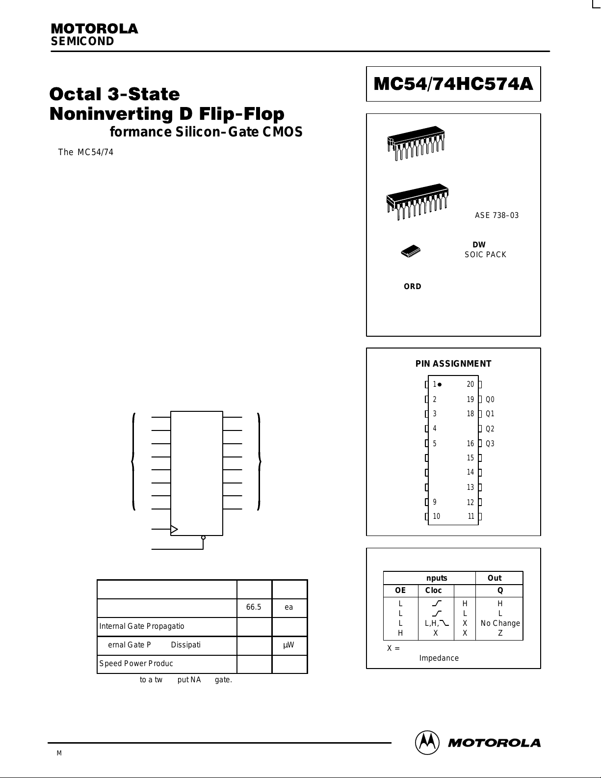
The MC54/74HC574A is identical in pinout to the LS574. The device
inputs are compatible with standard CMOS outputs; with pullup resistors,
they are compatible with LSTTL outputs.
Data meeting the setup time is clocked to the outputs with the rising edge
of the Clock. The Output Enable input does not affect the states of the
flip–flops, but when Output Enable is high, all device outputs are forced to
the high–impedance state. Thus, data may be stored even when the outputs
are not enabled.
The HC574A is identical in function to the HCT374A but has the flip–flop
inputs on the opposite side of the package from the outputs to facilitate PC
board layout.
The HC574A is the noninverting version of the HC564.
• Output Drive Capability: 15 LSTTL Loads
• Outputs Directly Interface to CMOS, NMOS and TTL
• Operating Voltage Range: 2.0 to 6.0 V
• Low Input Current: 1.0 µA
• In Compliance with the Requirements Defined by JEDEC Standard
No. 7A
• Chip Complexity: 266 FETs or 66.5 Equivalent Gates
J SUFFIX
20
1
20
1
20
1
ORDERING INFORMATION
MC54HCXXXAJ
MC74HCXXXAN
MC74HCXXXADW
PIN ASSIGNMENT
CERAMIC PACKAGE
CASE 732–03
N SUFFIX
PLASTIC PACKAGE
CASE 738–03
DW SUFFIX
SOIC PACKAGE
CASE 751D–04
Ceramic
Plastic
SOIC
LOGIC DIAGRAM
219
D0
3
D1
4
D2
DATA
INPUTS
CLOCK
OUTPUT ENABLE
ОООООООО
Internal Gate Count*
Internal Gate Propagation Delay
Internal Gate Power Dissipation
Speed Power Product
ОООООООО
*Equivalent to a two–input NAND gate.
5
D3
6
D4
7
D5
8
D6
9
D7
11
1
Design Criteria
Q0
18
Q1
17
Q2
16
Q3
15
Q4
14
Q5
13
Q6
12
Q7
PIN 20 = V
PIN 10 = GND
Value
ÎÎ
66.5
1.5
5.0
0.0075
ÎÎ
NON–
INVERTING
OUTPUTS
CC
Units
ÎÎ
ea
ns
µW
pJ
ÎÎ
OUTPUT
ENABLE
D0
D1
D2
D3 5
D4
D5
D6
D7
GND
1
2
3
4
6
7
8
9
10
20
19
18
17
16
15
14
13
12
11
V
CC
Q0
Q1
Q2
Q3
Q4
Q5
Q6
Q7
CLOCK
FUNCTION TABLE
Inputs Output
OE Clock D Q
LHH
LLL
L L,H, X No Change
HXXZ
X = Don’t Care
Z = High Impedance
3/97
Motorola, Inc. 1997
3–1
REV 7
MC54/74HC574A
Î
Î
Î
Î
Î
Î
Î
Î
Î
Î
Î
Î
Î
Î
Î
Î
Î
Î
Î
Î
Î
Î
Î
Î
Î
Î
Î
Î
Î
Î
Î
Î
Î
Î
Î
Î
Î
Î
Î
Î
Î
Î
Î
Î
Î
Î
Î
Î
Î
Î
Î
Î
Î
Î
Î
Î
Î
Î
Î
Î
Î
Î
Î
Î
Î
Î
Î
Î
Î
Î
Î
Î
Î
Î
Î
Î
Î
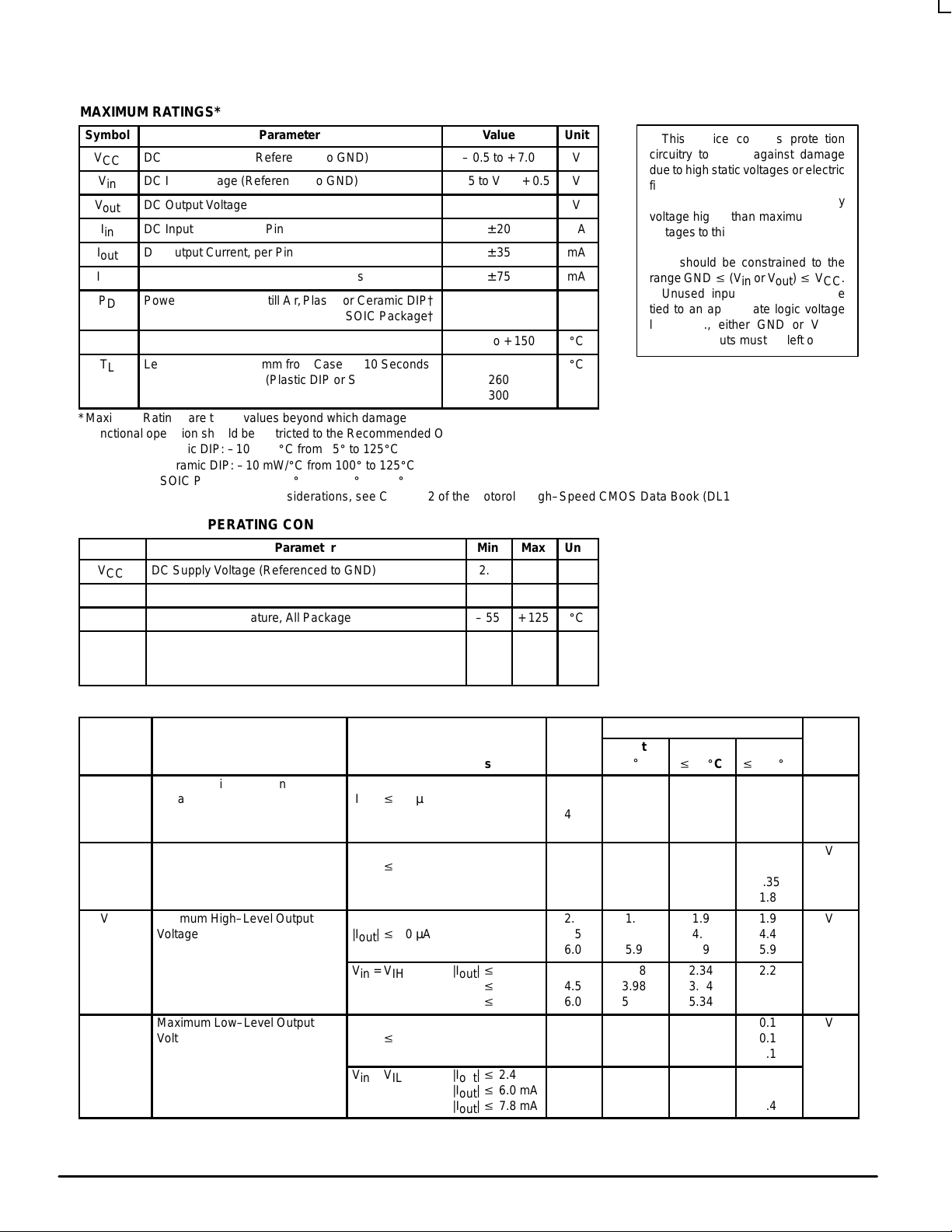
MAXIMUM RATINGS*
Symbol
V
V
I
I
Î
T
Î
DC Supply Voltage (Referenced to GND)
CC
V
DC Input Voltage (Referenced to GND)
in
DC Output Voltage (Referenced to GND)
out
I
DC Input Current, per Pin
in
DC Output Current, per Pin
out
DC Supply Current, VCC and GND Pins
CC
P
Power Dissipation in Still Air,Plastic or Ceramic DIP†
D
ОООООООООООО
Storage Temperature
stg
T
Lead Temperature, 1 mm from Case for 10 Seconds
L
ОООООООООООО
*Maximum Ratings are those values beyond which damage to the device may occur.
Functional operation should be restricted to the Recommended Operating Conditions.
†Derating — Plastic DIP: –10 mW/_C from 65_ to 125_C
Ceramic DIP: –10 mW/_C from 100_ to 125_C
SOIC Package: –7 mW/_C from 65_ to 125_C
For high frequency or heavy load considerations, see Chapter 2 of the Motorola High–Speed CMOS Data Book (DL129/D).
Parameter
SOIC Package†
(Plastic DIP or SOIC Package)
(Ceramic DIP)
Value
– 0.5 to + 7.0
– 0.5 to VCC + 0.5
– 0.5 to VCC + 0.5
± 20
± 35
± 75
750
500
ÎÎÎÎ
– 65 to + 150
260
ÎÎÎÎ
300
Unit
V
V
V
mA
mA
mA
mW
Î
_
C
_
C
Î
This device contains protection
circuitry to guard against damage
due to high static voltages or electric
fields. However, precautions must
be taken to avoid applications of any
voltage higher than maximum rated
voltages to this high–impedance circuit. For proper operation, Vin and
V
should be constrained to the
out
range GND v (Vin or V
Unused inputs must always be
tied to an appropriate logic voltage
level (e.g., either GND or VCC).
Unused outputs must be left open.
) v VCC.
out
RECOMMENDED OPERATING CONDITIONS
Symbol
V
CC
Vin, V
T
A
tr, t
ÎÎ
ÎÎ
DC Supply Voltage (Referenced to GND)
DC Input Voltage, Output Voltage (Referenced to GND)
out
Operating Temperature, All Package Types
Input Rise and Fall Time VCC = 2.0 V
f
ОООООООООООО
(Figure 1) VCC = 4.5 V
ОООООООООООО
Parameter
VCC = 6.0 V
Min
2.0
0
– 55
0
Î
0
0
Î
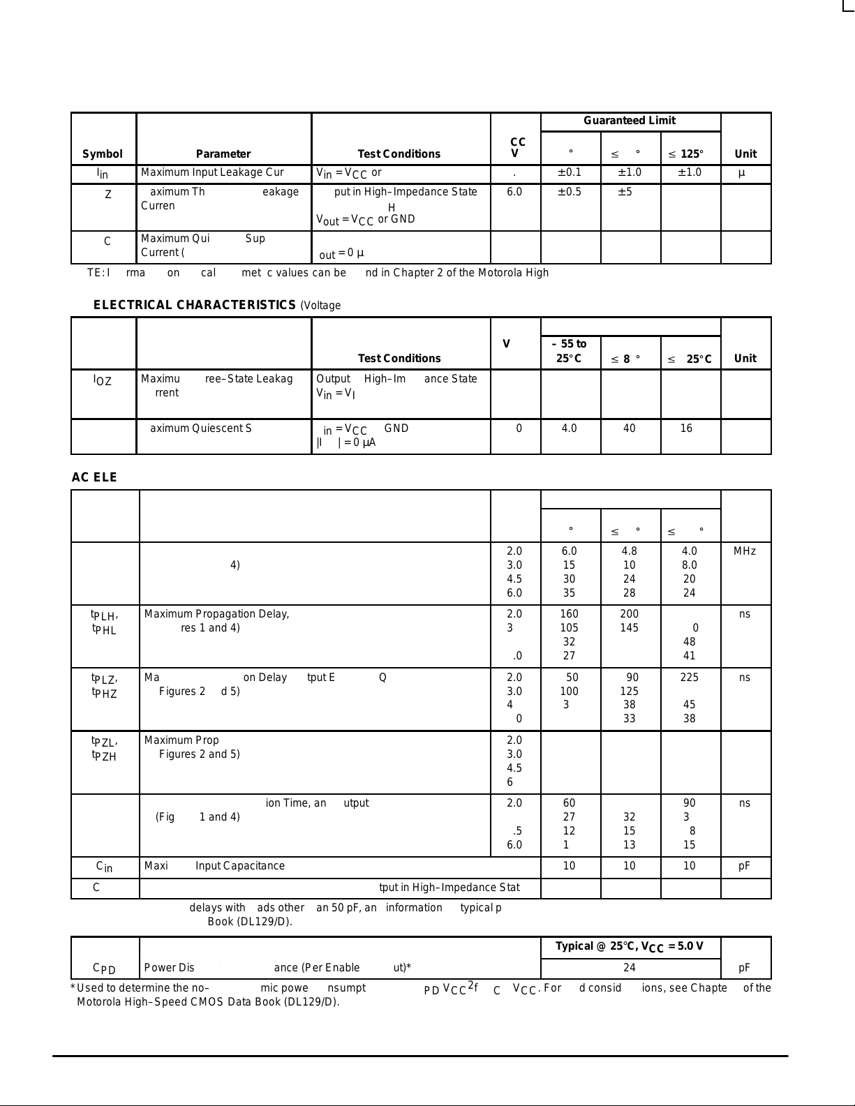
DC ELECTRICAL CHARACTERISTICS (Voltages Referenced to GND)
Symbol
V
ÎÎ
ÎÎ
V
ÎÎ
ÎÎ
V
OH
ÎÎ
ÎÎÎОООООООÎООООООО
V
OL
ÎÎ
ÎÎ
ÎÎÎОООООООÎООООООО
Minimum High–Level Input
IH
IL
ООООООО
Voltage
ООООООО
Maximum Low–Level Input
Voltage
ООООООО
ООООООО
Minimum High–Level Output
Voltage
ООООООО
Maximum Low–Level Output
ООООООО
Voltage
ООООООО
Parameter
Test Conditions
V
= VCC – 0.1 V
out
ООООООО
|I
| v 20 µA
out
ООООООО
V
= 0.1 V
out
|I
| v 20 µA
ООООООО
out
ООООООО
Vin = V
IH
|I
| v 20 µA
out
ООООООО
Vin = V
IH
Vin = V
IL
ООООООО
|I
| v 20 µA
out
ООООООО
Vin = V
IL
|I
| v 2.4 mA
out
|I
| v 6.0 mA
out
|I
| v 7.8 mA
out
|I
| v 2.4 mA
out
|I
| v 6.0 mA
out
|I
| v 7.8 mA
out
Max
6.0
V
CC
+ 125
1000
Î
500
400
Î
Unit
V
V
_
C
ns
Î
Î
V
CC
V
2.0
ÎÎ
3.0
4.5
ÎÎ
6.0
2.0
3.0
ÎÎ
4.5
ÎÎ
6.0
2.0
4.5
ÎÎ
6.0
3.0
4.5
ÎÎ
6.0
2.0
ÎÎ
4.5
6.0
ÎÎ
3.0
4.5
6.0
ÎÎ
Guaranteed Limit
– 55 to
25_C
1.5
ÎÎ
2.1
3.15
ÎÎ
4.2
0.5
0.9
ÎÎ
1.35
ÎÎ
1.8
1.9
4.4
ÎÎ
5.9
2.48
3.98
ÎÎ
5.48
0.1
ÎÎ
0.1
0.1
ÎÎ
0.26
0.26
0.26
ÎÎ
v
85_C
1.5
ÎÎ
2.1
3.15
ÎÎ
4.2
0.5
0.9
ÎÎ
1.35
ÎÎ
1.8
1.9
4.4
ÎÎ
5.9
2.34
3.84
ÎÎ
5.34
0.1
ÎÎ
0.1
0.1
ÎÎ
0.33
0.33
0.33
ÎÎ
v
125_C
1.5
ÎÎ
2.1
3.15
ÎÎ
4.2
0.5
0.9
ÎÎ
1.35
ÎÎ
1.8
1.9
4.4
ÎÎ
5.9
2.2
3.7
ÎÎ
5.2
0.1
ÎÎ
0.1
0.1
ÎÎ
0.4
0.4
0.4
ÎÎ
Unit
V
Î
Î
V
Î
Î
V
Î
Î
V
Î
Î
Î
MOTOROLA High–Speed CMOS Logic Data
3–2
DL129 — Rev 6
MC54/74HC574A
Î
Î
Î
Î
Î
Î
Î
Î
Î
Î
Î
Î
Î
Î
Î
Î
Î
Î
Î
Î
Î
Î
Î
Î
Î
Î
Î
Î
Î
Î
Î
Î
Î
Î
Î
Î
Î
Î
Î
Î
Î
Î
Î
Î
Î
Î
Î
Î
Î
Î
Î
Î
Î
Î
Î
Î
Î
Î
Î
Î
Î
Î
Î
Î
Î
Î
Î
Î
Î
Î
Î
Î
Î
Î
Î
Î
Î
Î
Î
Î
Î
Î
Î
Î
Î
Î
Î
Î
DC ELECTRICAL CHARACTERISTICS (Voltages Referenced to GND)
Guaranteed Limit
CC
V
CC
V
– 55 to
25_C
± 0.1
± 0.5
ÎÎ
ÎÎ
4.0
Guaranteed Limit
– 55 to
25_C
± 0.5
ÎÎ
ÎÎ
4.0
ÎÎ
v
85_C
± 1.0
± 5.0
ÎÎ
ÎÎ
40
v
85_C
± 5.0
ÎÎ
ÎÎ
40
ÎÎ
v
125_C
± 1.0
± 10
ÎÎ
ÎÎ
160
v
125_C
± 10
ÎÎ
ÎÎ
160
ÎÎ
V
Symbol
I
in
I
OZ
ÎÎ
ÎÎ
I
CC
Parameter
Maximum Input Leakage Current
Maximum Three–State Leakage
ООООООО
Current
ООООООО
Maximum Quiescent Supply
Current (per Package)
Test Conditions
Vin = VCC or GND
Output in High–Impedance State
ООООООО
Vin = VIL or V
V
= VCC or GND
out
ООООООО
IH
Vin = VCC or GND
I
= 0 µA
out
6.0
6.0
ÎÎ
ÎÎ
6.0
NOTE:Information on typical parametric values can be found in Chapter 2 of the Motorola High–Speed CMOS Data Book (DL129/D).
DC ELECTRICAL CHARACTERISTICS (Voltages Referenced to GND)
V
Symbol
I
OZ
ÎÎ
ÎÎ
I
CC
ÎÎ
Maximum Three–State Leakage
Current
ООООООО
ООООООО
Maximum Quiescent Supply
ООООООО
Current (per Package)
Parameter
Test Conditions
Output in High–Impedance State
Vin = VIL or V
ООООООО
V
= VCC or GND
out
ООООООО
Vin = VCC or GND
ООООООО
|I
| = 0 µA
out
IH
6.0
ÎÎ
ÎÎ
6.0
ÎÎ
Unit
µA
µA
Î
Î
µA
Unit
µA
Î
Î
µA
Î
AC ELECTRICAL CHARACTERISTICS (C
= 50 pF, Input tr = tf = 6.0 ns)
L
Guaranteed Limit
Symbol
f
max
ÎÎ
ÎÎ
t
,
PLH
t
ÎÎ
PHL
ÎÎ
t
,
PLZ
t
PHZ
ÎÎ
ÎÎ
t
,
PZL
t
PZH
ÎÎ
ÎÎ
t
,
TLH
t
THL
ÎÎ
ÎÎ
C
in
C
out
V
CC
Parameter
Maximum Clock Frequency (50% Duty Cycle)
(Figures 1 and 4)
ООООООООООООООО
ООООООООООООООО
Maximum Propagation Delay, Clock to Q
(Figures 1 and 4)
ООООООООООООООО
ООООООООООООООО
Maximum Propagation Delay, Output Enable to Q
(Figures 2 and 5)
ООООООООООООООО
ООООООООООООООО
Maximum Propagation Delay, Output Enable to Q
(Figures 2 and 5)
ООООООООООООООО
ООООООООООООООО
Maximum Output Transition Time, any Output
(Figures 1 and 4)
ООООООООООООООО
ООООООООООООООО
2.0
3.0
ÎÎ
4.5
ÎÎ
6.0
2.0
3.0
ÎÎ
4.5
ÎÎ
6.0
2.0
3.0
ÎÎ
4.5
ÎÎ
6.0
2.0
3.0
ÎÎ
4.5
ÎÎ
6 0
2.0
3.0
ÎÎ
4.5
ÎÎ
6.0
Maximum Input Capacitance
Maximum Three–State Output Capacitance, Output in High–Impedance State
– 55 to
V
25_C
6.0
15
ÎÎ
30
ÎÎ
35
160
105
ÎÎ
32
ÎÎ
27
150
100
ÎÎ
30
ÎÎ
26
140
90
ÎÎ
28
ÎÎ
24
60
27
ÎÎ
12
ÎÎ
10
10
15
v
85_C
4.8
10
ÎÎ
24
ÎÎ
28
200
145
ÎÎ
40
ÎÎ
34
190
125
ÎÎ
38
ÎÎ
33
175
120
ÎÎ
35
ÎÎ
30
75
32
ÎÎ
15
ÎÎ
13
10
15
v
125_C
4.0
8.0
ÎÎ
20
ÎÎ
24
240
190
ÎÎ
48
ÎÎ
41
225
150
ÎÎ
45
ÎÎ
38
210
140
ÎÎ
42
ÎÎ
36
90
36
ÎÎ
18
ÎÎ
15
10
15
Unit
MHz
Î
Î
ns
Î
Î
ns
Î
Î
ns
Î
Î
ns
Î
Î
pF
pF
NOTE:For propagation delays with loads other than 50 pF , and information on typical parametric values, see Chapter 2 of the Motorola High–
Speed CMOS Data Book (DL129/D).
C
PD
Power Dissipation Capacitance (Per Enabled Output)*
*Used to determine the no–load dynamic power consumption: PD = CPD V
Motorola High–Speed CMOS Data Book (DL129/D).
High–Speed CMOS Logic Data
DL129 — Rev 6
Typical @ 25°C, VCC = 5.0 V
24
2
f + ICC VCC. For load considerations, see Chapter 2 of the
CC
pF
3–3 MOTOROLA
 Loading...