

Motorola MC54HC541AJ, MC74HC541AN Datasheet
SEMICONDUCTOR TECHNICAL DATA
3–1
REV 1
Motorola, Inc. 1995
10/95
"
! "
"
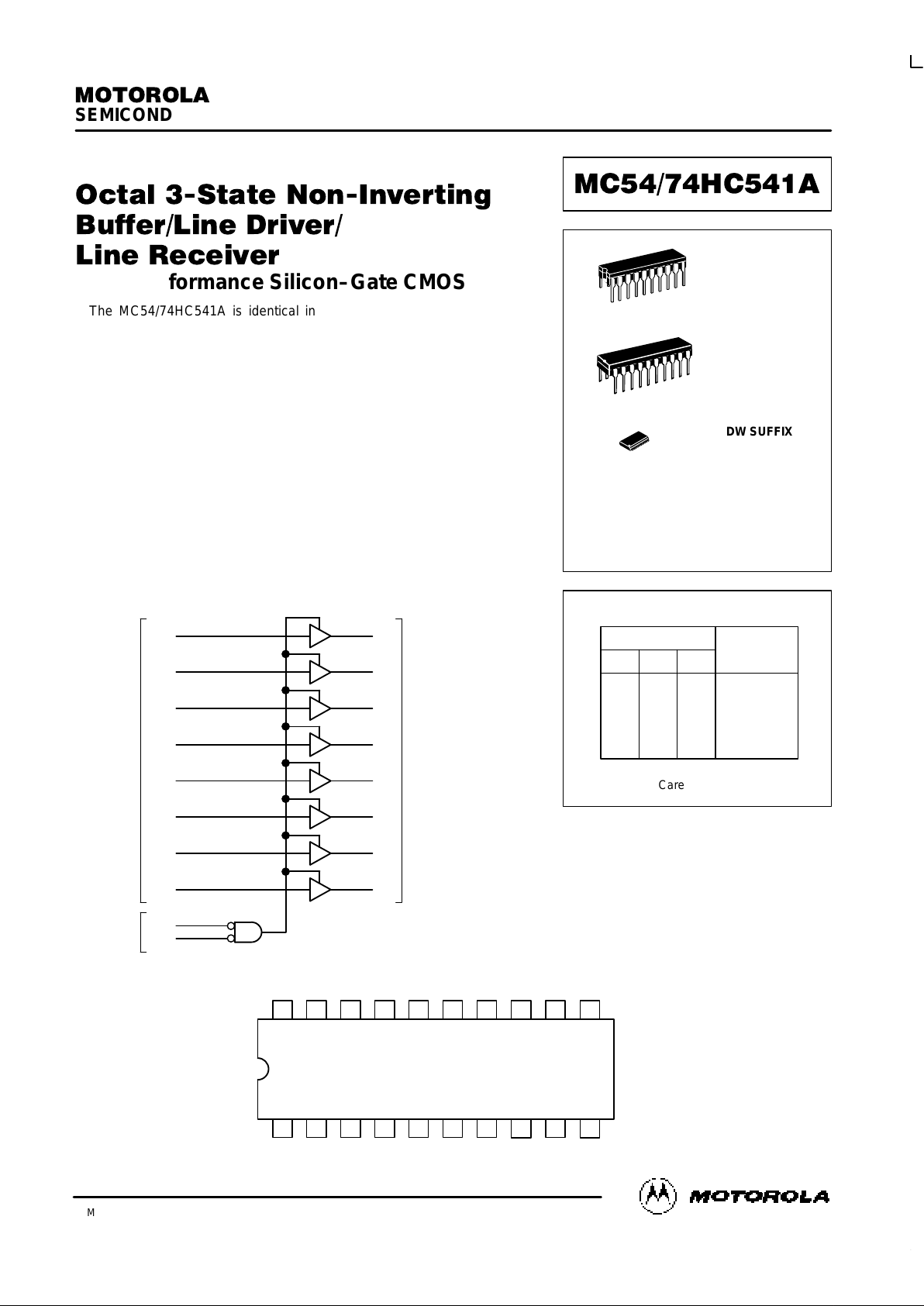
High–Performance Silicon–Gate CMOS
The MC54/74HC541A is identical in pinout to the LS541. The device
inputs a re compatible w ith Standard CMOS o utputs. E xternal p ullup
resistors make them compatible with LSTTL outputs.
The HC541A is an octal non–inverting buffer/line driver/line receiver
designed to be used with 3–state memory address drivers, clock drivers, and
other bus–oriented systems. This device features inputs and outputs on
opposite sides of the package and two ANDed active–low output enables.
The HC541A is similar in function to the HC540A, which has inverting
outputs.
• Output Drive Capability: 15 LSTTL Loads
• Outputs Directly Interface to CMOS, NMOS and TTL
• Operating Voltage Range: 2 to 6V
• Low Input Current: 1µA
• High Noise Immunity Characteristic of CMOS Devices
• In Compliance With the JEDEC Standard No. 7A Requirements
• Chip Complexity: 134 FETs or 33.5 Equivalent Gates
18
Y1
2
A1
17
Y2
3
A2
16
Y3
4
A3
15
Y4
5
A4
14
Y5
6
A5
13
Y6
7
A6
12
Y7
8
A7
11
Y8
9
A8
OE1
OE2
1
19
Output
Enables
Data
Inputs
Non–Inverting
Outputs
PIN 20 = V
CC
PIN 10 = GND
LOGIC DIAGRAM
Pinout: 20–Lead Packages (Top View)
1920 18 17 16 15 14
21 3 4 5 6 7
V
CC
13
8
12
9
11
10
OE2 Y1 Y2 Y3 Y4 Y5 Y6 Y7 Y8
OE1 A1 A2 A3 A4 A5 A6 A7 A8 GND
L
L
H
X
L
L
X
H
L
H
X
X
FUNCTION TABLE
Inputs
Output Y
OE1 OE2 A
L
H
Z
Z
Z = High Impedance
X = Don’t Care
DW SUFFIX
SOIC PACKAGE
CASE 751D–04
N SUFFIX
PLASTIC PACKAGE
CASE 738–03
ORDERING INFORMATION
MC54HCXXXAJ
MC74HCXXXAN
MC74HCXXXADW
Ceramic
Plastic
SOIC
J SUFFIX
CERAMIC PACKAGE
CASE 732–03
1
20
1
20
1
20
MC54/74HC541A
MOTOROLA High–Speed CMOS Logic Data
DL129 — Rev 6
3–2
MAXIMUM RATINGS*
Symbol
Parameter
Value
Unit
V
CC
DC Supply Voltage (Referenced to GND)
– 0.5 to + 7.0
V
V
in
DC Input Voltage (Referenced to GND)
– 0.5 to VCC + 0.5
V
V
out
DC Output Voltage (Referenced to GND)
– 0.5 to VCC + 0.5
V
I
in
DC Input Current, per Pin
± 20
mA
I
out
DC Output Current, per Pin
± 35
mA
I
CC
DC Supply Current, VCC and GND Pins
± 75
mA
P
D
Power Dissipation in Still Air,Plastic or Ceramic DIP†
SOIC Package†
750
500
mW
T
stg
Storage Temperature Range
– 65 to + 150
_
C
T
L
Lead Temperature, 1 mm from Case for 10 Seconds
Plastic DIP or SOIC Package
Ceramic DIP)
260
300
_
C
*Maximum Ratings are those values beyond which damage to the device may occur.
Functional operation should be restricted to the Recommended Operating Conditions.
†Derating — Plastic DIP: – 10 mW/_C from 65_ to 125_C
Ceramic DIP: – 10 mW/_C from 100_ to 125_C
SOIC Package: – 7 mW/_C from 65_ to 125_C
For high frequency or heavy load considerations, see Chapter 2 of the Motorola High–Speed CMOS Data Book (DL129/D).
RECOMMENDED OPERATING CONDITIONS
Symbol
Parameter
Min
Max
Unit
V
CC
DC Supply Voltage (Referenced to GND)
2.0
6.0
V
Vin, V
out
DC Input Voltage, Output Voltage (Referenced to GND)
0
V
CC
V
T
A
Operating Temperature Range, All Package Types
– 55
+ 125
_
C
tr, t
f
Input Rise/Fall Time VCC = 2.0 V
(Figure 1) VCC = 4.5 V
VCC = 6.0 V
0
0
0
1000
500
400
ns
DC CHARACTERISTICS (Voltages Referenced to GND)
V
Guaranteed Limit
Symbol Parameter Condition
V
CC
V
–55 to 25°C ≤85°C ≤125°C Unit
V
IH
Minimum High–Level Input Voltage V
out
= 0.1V
|I
out
| ≤ 20µA
2.0
3.0
4.5
6.0
1.50
2.10
3.15
4.20
1.50
2.10
3.15
4.20
1.50
2.10
3.15
4.20
V
V
IL
Maximum Low–Level Input Voltage V
out
= VCC – 0.1V
|I
out
| ≤ 20µA
2.0
3.0
4.5
6.0
0.50
0.90
1.35
1.80
0.50
0.90
1.35
1.80
0.50
0.90
1.35
1.80
V
V
OH
Minimum High–Level Output
Voltage
Vin = V
IL
|I
out
| ≤ 20µA
2.0
4.5
6.0
1.9
4.4
5.9
1.9
4.4
5.9
1.9
4.4
5.9
V
Vin = V
IL
|I
out
| ≤ 3.6mA
|I
out
| ≤ 6.0mA
|I
out
| ≤ 7.8mA
3.0
4.5
6.0
2.48
3.98
5.48
2.34
3.84
5.34
2.20
3.70
5.20
V
OL
Maximum Low–Level Output
Voltage
Vin = V
IH
|I
out
| ≤ 20µA
2.0
4.5
6.0
0.1
0.1
0.1
0.1
0.1
0.1
0.1
0.1
0.1
V
Vin = V
IH
|I
out
| ≤ 3.6mA
|I
out
| ≤ 6.0mA
|I
out
| ≤ 7.8mA
3.0
4.5
6.0
0.26
0.26
0.26
0.33
0.33
0.33
0.40
0.40
0.40
This device contains protection
circuitry to guard against damage
due to high static voltages or electric
fields. However, precautions must
be taken to avoid applications of any
voltage higher than maximum rated
voltages to this high–impedance circuit. For proper operation, Vin and
V
out
should be constrained to the
range GND v (Vin or V
out
) v VCC.
Unused inputs must always be
tied to an appropriate logic voltage
level (e.g., either GND or VCC).
Unused outputs must be left open.
 Loading...