

Motorola MC54HC4060AJ, MC74HC4060ADT, MC74HC4060AD Datasheet
SEMICONDUCTOR TECHNICAL DATA
3–1
REV 6
Motorola, Inc. 1995
10/95
3–1
REV 1
Motorola, Inc. 1996
3/96
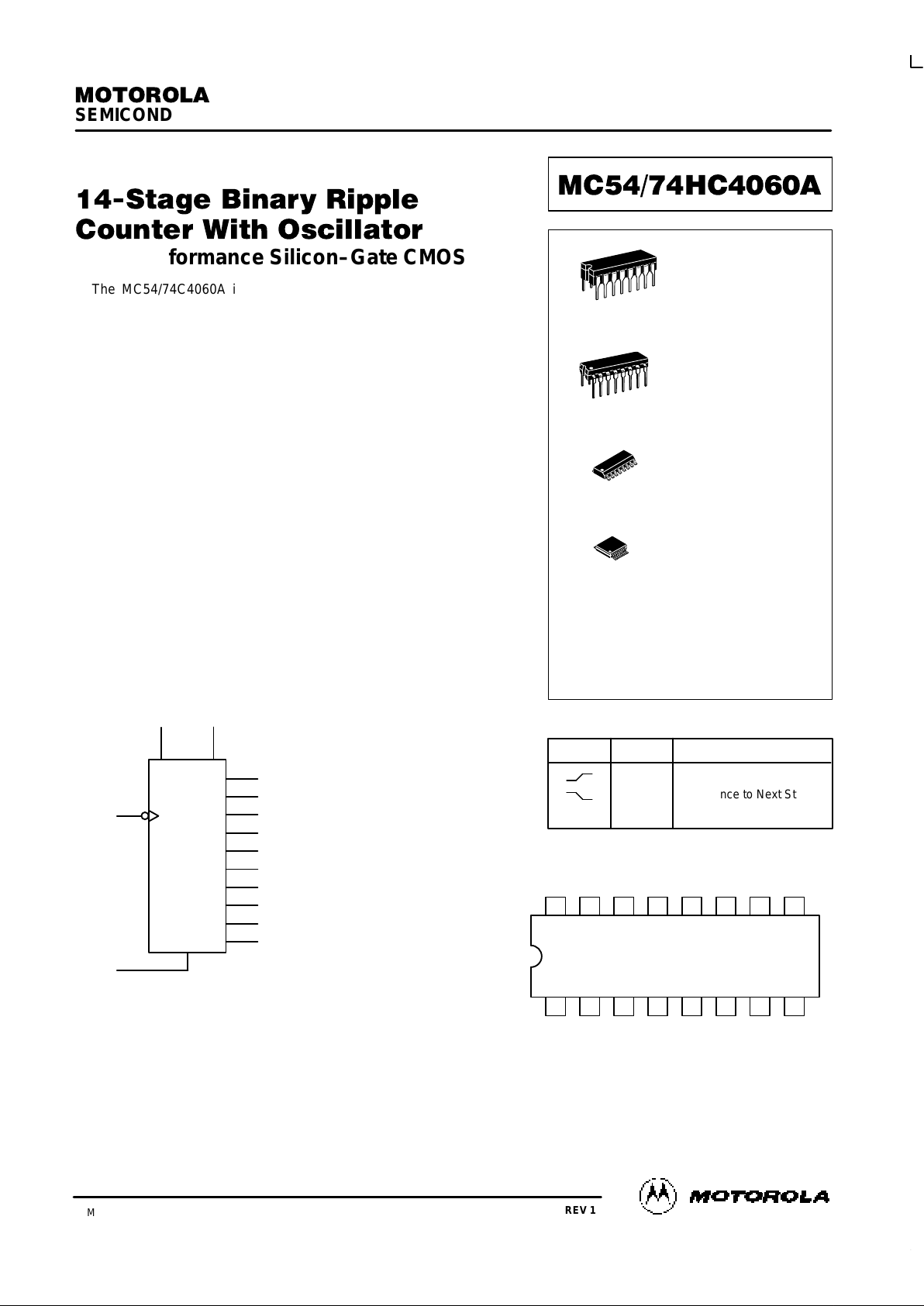
! #
"! ! !
High–Performance Silicon–Gate CMOS
The MC54/74C4060A is identical in pinout to the standard CMOS
MC14060B. The device inputs are compatible with standard CMOS outputs; with pullup resistors, they are compatible with LSTTL outputs.
This device consists of 14 master–slave flip–flops and an oscillator
with a frequency that is controlled either by a crystal or by an RC circuit
connected externally. The output of each flip–flop feeds the next and the
frequency at each output is half of that of the preceding one. The state of
the counter advances on the negative–going edge of the Osc In. The
active–high Reset is asynchronous and disables the oscillator to allow
very low power consumption during stand–by operation.
State changes of the Q outputs do not occur simultaneously because
of internal ripple delays. Therefore, decoded output signals are subject to
decoding spikes and may have to be gated with Osc Out 2 of the
HC4060A.
• Output Drive Capability: 10 LSTTL Loads
• Outputs Directly Interface to CMOS, NMOS, and TTL
• Operating Voltage Range: 2 to 6 V
• Low Input Current: 1 µA
• High Noise Immunity Characteristic of CMOS Devices
• In Compliance With JEDEC Standard No. 7A Requirements
• Chip Complexity: 390 FETs or 97.5 Equivalent Gates
LOGIC DIAGRAM
Q4
7
Q5
5
Q6
4
Q7
6
Q8
14
Q9
13
Q10
15
Q12
1
Q13
2
Q14
3
Osc In
11
Reset
12
Pin 16 = V
CC
Pin 8 = GND
Osc Out 1 Osc Out 2
910
1516 14 13 12 11 10
21 3 4 5 6 7
V
CC
9
8
Q10 Q8 Q9 Reset Osc In
Osc
Out 1
Osc
Out 2
Q12 Q13 Q14 Q6 Q5 Q7 Q4
GND
Pinout: 16–Lead Plastic Package (Top View)
FUNCTION TABLE
Clock Reset Output State
X
L
L
H
No Charge
Advance to Next State
All Outputs Are Low
D SUFFIX
SOIC PACKAGE
CASE 751B–05
N SUFFIX
PLASTIC PACKAGE
CASE 648–08
1
16
1
16
J SUFFIX
CERAMIC PACKAGE
CASE 620–10
1
16
ORDERING INFORMATION
MC54HCXXXXAJ
MC74HCXXXXAN
MC74HCXXXXAD
MC74HCXXXXADT
Ceramic
Plastic
SOIC
TSSOP
1
16
DT SUFFIX
TSSOP PACKAGE
CASE 748C–03
MC54/74HC4060A
MOTOROLA High–Speed CMOS Logic Data
DL129 — Rev 6
3–2
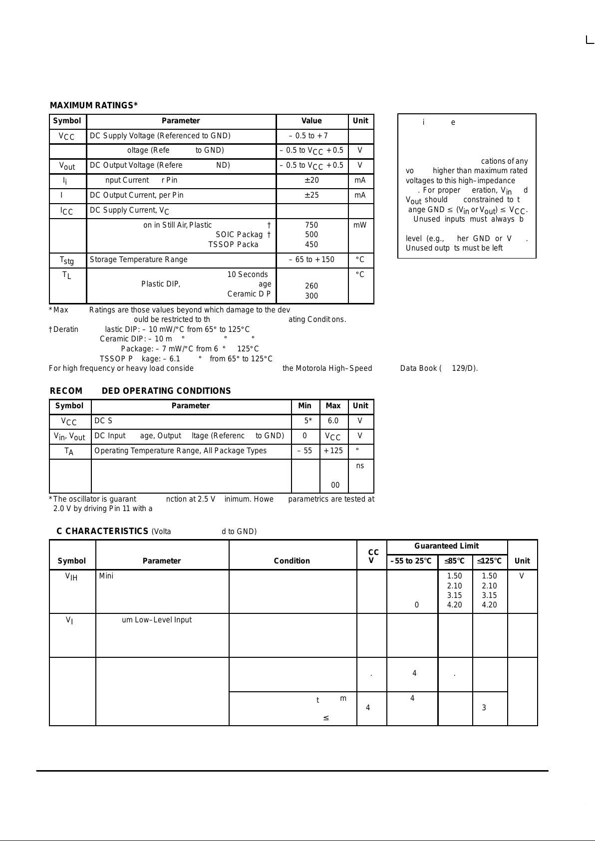
MAXIMUM RATINGS*
Symbol
Parameter
Value
Unit
V
CC
DC Supply Voltage (Referenced to GND)
– 0.5 to + 7.0
V
V
in
DC Input Voltage (Referenced to GND)
– 0.5 to VCC + 0.5
V
V
out
DC Output Voltage (Referenced to GND)
– 0.5 to VCC + 0.5
V
I
in
DC Input Current, per Pin
± 20
mA
I
out
DC Output Current, per Pin
± 25
mA
I
CC
DC Supply Current, VCC and GND Pins
± 50
mA
P
D
Power Dissipation in Still Air,Plastic or Ceramic DIP†
SOIC Package†
TSSOP Package†
750
500
450
mW
T
stg
Storage Temperature Range
– 65 to + 150
_
C
T
L
Lead Temperature, 1 mm from Case for 10 Seconds
Plastic DIP, SOIC or TSSOP Package
Ceramic DIP
260
300
_
C
*Maximum Ratings are those values beyond which damage to the device may occur.
Functional operation should be restricted to the Recommended Operating Conditions.
†Derating — Plastic DIP: – 10 mW/_C from 65_ to 125_C
Ceramic DIP: – 10 mW/_C from 100_ to 125_C
SOIC Package: – 7 mW/_C from 65_ to 125_C
TSSOP Package: – 6.1 mW/_C from 65_ to 125_C
For high frequency or heavy load considerations, see Chapter 2 of the Motorola High–Speed CMOS Data Book (DL129/D).
RECOMMENDED OPERATING CONDITIONS
Symbol
Parameter
Min
Max
Unit
V
CC
DC Supply Voltage (Referenced to GND)
2.5*
6.0
V
Vin, V
out
DC Input Voltage, Output Voltage (Referenced to GND)
0
V
CC
V
T
A
Operating Temperature Range, All Package Types
– 55
+ 125
_
C
tr, t
f
Input Rise/Fall Time VCC = 2.0 V
(Figure 1) VCC = 4.5 V
VCC = 6.0 V
0
0
0
1000
500
400
ns
*The oscillator is guaranteed to function at 2.5 V minimum. However, parametrics are tested at
2.0 V by driving Pin 11 with an external clock source.
DC CHARACTERISTICS (Voltages Referenced to GND)
V
Guaranteed Limit
Symbol
Parameter
Condition
V
CC
V
–55 to 25°C ≤85°C ≤125°C
Unit
V
IH
Minimum High–Level Input Voltage V
out
= 0.1V or VCC –0.1V
|I
out
| ≤ 20µA
2.0
3.0
4.5
6.0
1.50
2.10
3.15
4.20
1.50
2.10
3.15
4.20
1.50
2.10
3.15
4.20
V
V
IL
Maximum Low–Level Input Voltage V
out
= 0.1V or VCC – 0.1V
|I
out
| ≤ 20µA
2.0
3.0
4.5
6.0
0.50
0.90
1.35
1.80
0.50
0.90
1.35
1.80
0.50
0.90
1.35
1.80
V
V
OH
Minimum High–Level Output
Voltage (Q4–Q10, Q12–Q14)
Vin = VIH or V
IL
|I
out
| ≤ 20µA
2.0
4.5
6.0
1.9
4.4
5.9
1.9
4.4
5.9
1.9
4.4
5.9
V
Vin =VIH or V
IL
|I
out
| ≤ 2.4mA
|I
out
| ≤ 4.0mA
|I
out
| ≤ 5.2mA
3.0
4.5
6.0
2.48
3.98
5.48
2.34
3.84
5.34
2.20
3.70
5.20
This device contains protection
circuitry to guard against damage
due to high static voltages or electric
fields. However, precautions must
be taken to avoid applications of any
voltage higher than maximum rated
voltages to this high–impedance circuit. For proper operation, Vin and
V
out
should be constrained to the
range GND v (Vin or V
out
) v VCC.
Unused inputs must always be
tied to an appropriate logic voltage
level (e.g., either GND or VCC).
Unused outputs must be left open.
MC54/74HC4060A
High–Speed CMOS Logic Data
DL129 — Rev 6
3–3 MOTOROLA
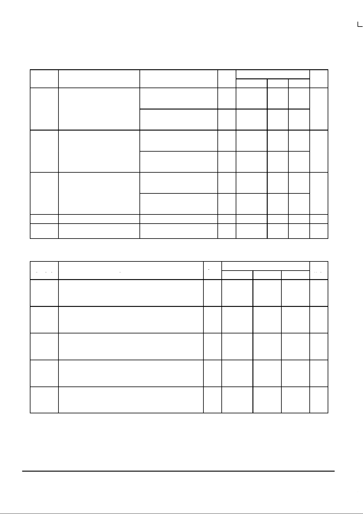
DC CHARACTERISTICS (Voltages Referenced to GND)
Symbol Unit
Guaranteed Limit
V
CC
V
ConditionParameter
Symbol Unit≤125°C≤85°C–55 to 25°C
V
CC
V
ConditionParameter
V
OL
Maximum Low–Level Output
Voltage (Q4–Q10, Q12–Q14)
Vin = VIH or V
IL
|I
out
| ≤ 20µA
2.0
4.5
6.0
0.1
0.1
0.1
0.1
0.1
0.1
0.1
0.1
0.1
V
Vin = VIH or V
IL
|I
out
| ≤ 2.4mA
|I
out
| ≤ 4.0mA
|I
out
| ≤ 5.2mA
3.0
4.5
6.0
0.26
0.26
0.26
0.33
0.33
0.33
0.40
0.40
0.40
V
OH
Minimum High–Level Output
Voltage (Osc Out 1, Osc Out 2)
Vin = VCC or GND
|I
out
| ≤ 20µA
2.0
4.5
6.0
1.9
4.4
5.9
1.9
4.4
5.9
1.9
4.4
5.9
V
Vin =VCC or GND |I
out
| ≤ 0.7mA
|I
out
| ≤ 1.0mA
|I
out
| ≤ 1.3mA
3.0
4.5
6.0
2.48
3.98
5.48
2.34
3.84
5.34
2.20
3.70
5.20
V
OL
Maximum Low–Level Output
Voltage (Osc Out 1, Osc Out 2)
Vin = VCC or GND
|I
out
| ≤ 20µA
2.0
4.5
6.0
0.1
0.1
0.1
0.1
0.1
0.1
0.1
0.1
0.1
V
Vin =VCC or GND |I
out
| ≤ 0.7mA
|I
out
| ≤ 1.0mA
|I
out
| ≤ 1.3mA
3.0
4.5
6.0
0.26
0.26
0.26
0.33
0.33
0.33
0.40
0.40
0.40
I
in
Maximum Input Leakage Current Vin = VCC or GND 6.0 ±0.1 ±1.0 ±1.0 µA
I
CC
Maximum Quiescent Supply
Current (per Package)
Vin = VCC or GND
I
out
= 0µA
6.0 4 40 160 µA
NOTE: Information on typical parametric values can be found in Chapter 2 of the Motorola High–Speed CMOS Data Book (DL129/D).
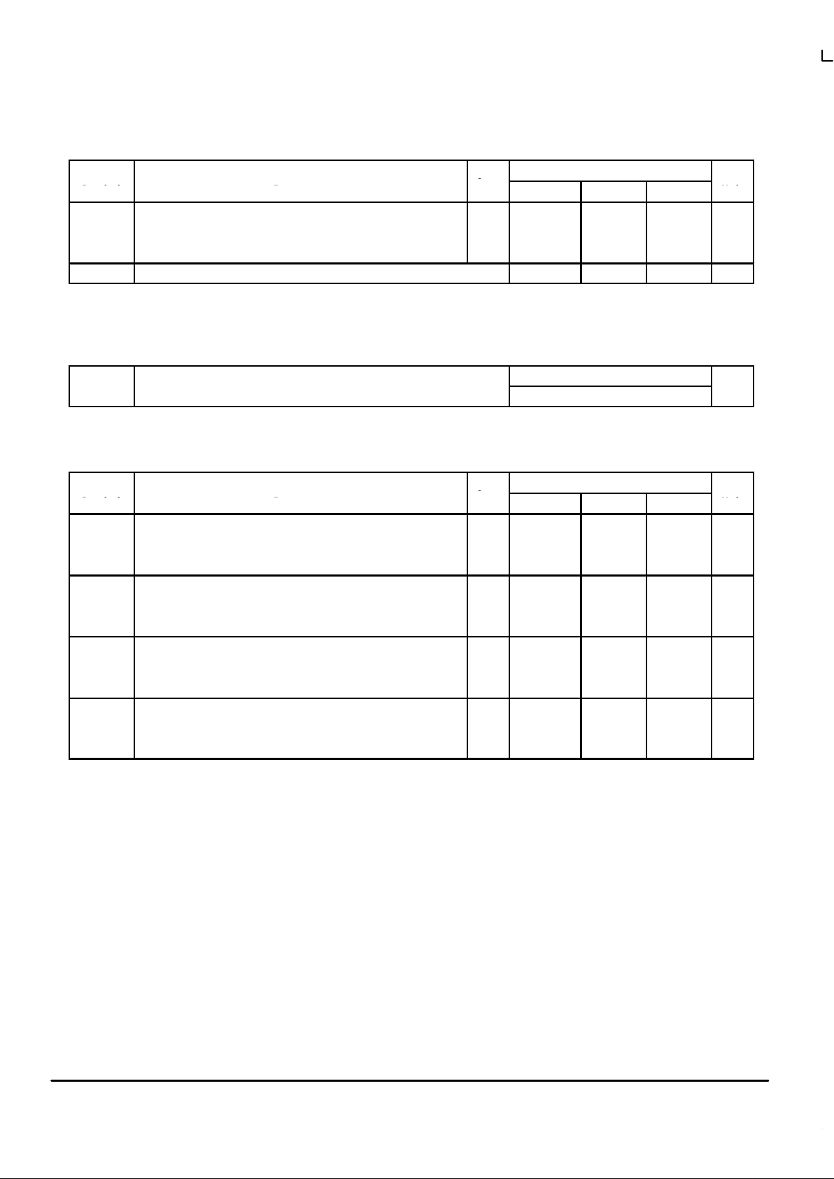
AC CHARACTERISTICS (C
L
= 50 pF, Input tr = tf = 6 ns)
V
Guaranteed Limit
Symbol
Parameter
V
CC
V
–55 to 25°C ≤85°C ≤125°C
Unit
f
max
Maximum Clock Frequency (50% Duty Cycle)
(Figures 1 and 4)
2.0
3.0
4.5
6.0
6.0
10
30
50
9.0
14
28
45
8.0
12
25
40
MHz
t
PLH
,
t
PHL
Maximum Propagation Delay, Osc In to Q4*
(Figures 1 and 4)
2.0
3.0
4.5
6.0
300
180
60
51
375
200
75
64
450
250
90
75
ns
t
PLH
,
t
PHL
Maximum Propagation Delay, Osc In to Q14*
(Figures 1 and 4)
2.0
3.0
4.5
6.0
500
350
250
200
750
450
275
220
1000
600
300
250
ns
t
PHL
Maximum Propagation Delay, Reset to Any Q
(Figures 2 and 4)
2.0
3.0
4.5
6.0
195
75
39
33
245
100
49
42
300
125
61
53
ns
t
PLH
,
t
PHL
Maximum Propagation Delay, Qn to Qn+1
(Figures 3 and 4)
2.0
3.0
4.5
6.0
75
60
15
13
95
75
19
16
125
95
24
20
ns
MC54/74HC4060A
MOTOROLA High–Speed CMOS Logic Data
DL129 — Rev 6
3–4
AC CHARACTERISTICS (C
L
= 50 pF, Input tr = tf = 6 ns) – continued
V
Guaranteed Limit
Symbol
Parameter
V
CC
V
–55 to 25°C ≤85°C ≤125°C
Unit
t
TLH
,
t
THL
Maximum Output Transition Time, Any Output
(Figures 1 and 4)
2.0
3.0
4.5
6.0
75
27
15
13
95
32
19
16
110
36
22
19
ns
C
in
Maximum Input Capacitance 10 10 10 pF
NOTE: For propagation delays with loads other than 50 pF, and information on typical parametric values, see Chapter 2 of the Motorola High–
Speed CMOS Data Book (DL129/D).
* For TA = 25°C and CL = 50 pF, typical propagation delay from Clock to other Q outputs may be calculated with the following equations:
VCC = 2.0 V: tP = [93.7 + 59.3 (n–1)] ns VCC = 4.5 V: tP = [30.25 + 14.6 (n–1)] ns
VCC = 3.0 V: tP = [61.5+ 34.4 (n–1)] ns VCC = 6.0 V: tP = [24.4 + 12 (n–1)] ns
Typical @ 25°C, VCC = 5.0 V
C
PD
Power Dissipation Capacitance (Per Package)*
35
pF
*Used to determine the no–load dynamic power consumption: PD = CPD V
CC
2
f + ICC VCC. For load considerations, see Chapter 2 of the
Motorola High–Speed CMOS Data Book (DL129/D).
TIMING REQUIREMENTS (Input t
r
= tf = 6 ns)
V
Guaranteed Limit
Symbol
Parameter
V
CC
V
–55 to 25°C ≤85°C ≤125°C
Unit
t
rec
Minimum Recovery Time, Reset Inactive to Clock
(Figure 2)
2.0
3.0
4.5
6.0
100
75
20
17
125
100
25
21
150
120
30
25
ns
t
w
Minimum Pulse Width, Clock
(Figure 1)
2.0
3.0
4.5
6.0
75
27
15
13
95
32
19
16
110
36
23
19
ns
t
w
Minimum Pulse Width, Reset
(Figure 2)
2.0
3.0
4.5
6.0
75
27
15
13
95
32
19
16
110
36
23
19
ns
tr, t
f
Maximum Input Rise and Fall Times
(Figure 1)
2.0
3.0
4.5
6.0
1000
800
500
400
1000
800
500
400
1000
800
500
400
ns
NOTE: Information on typical parametric values can be found in Chapter 2 of the Motorola High–Speed CMOS Data Book (DL129/D).
 Loading...