

MOTOROLA MC34184DR2, MC34184DTBR2, MC34182P, MC34182DR2, MC34181DR2 Datasheet
...
Order this document by MC34181/D
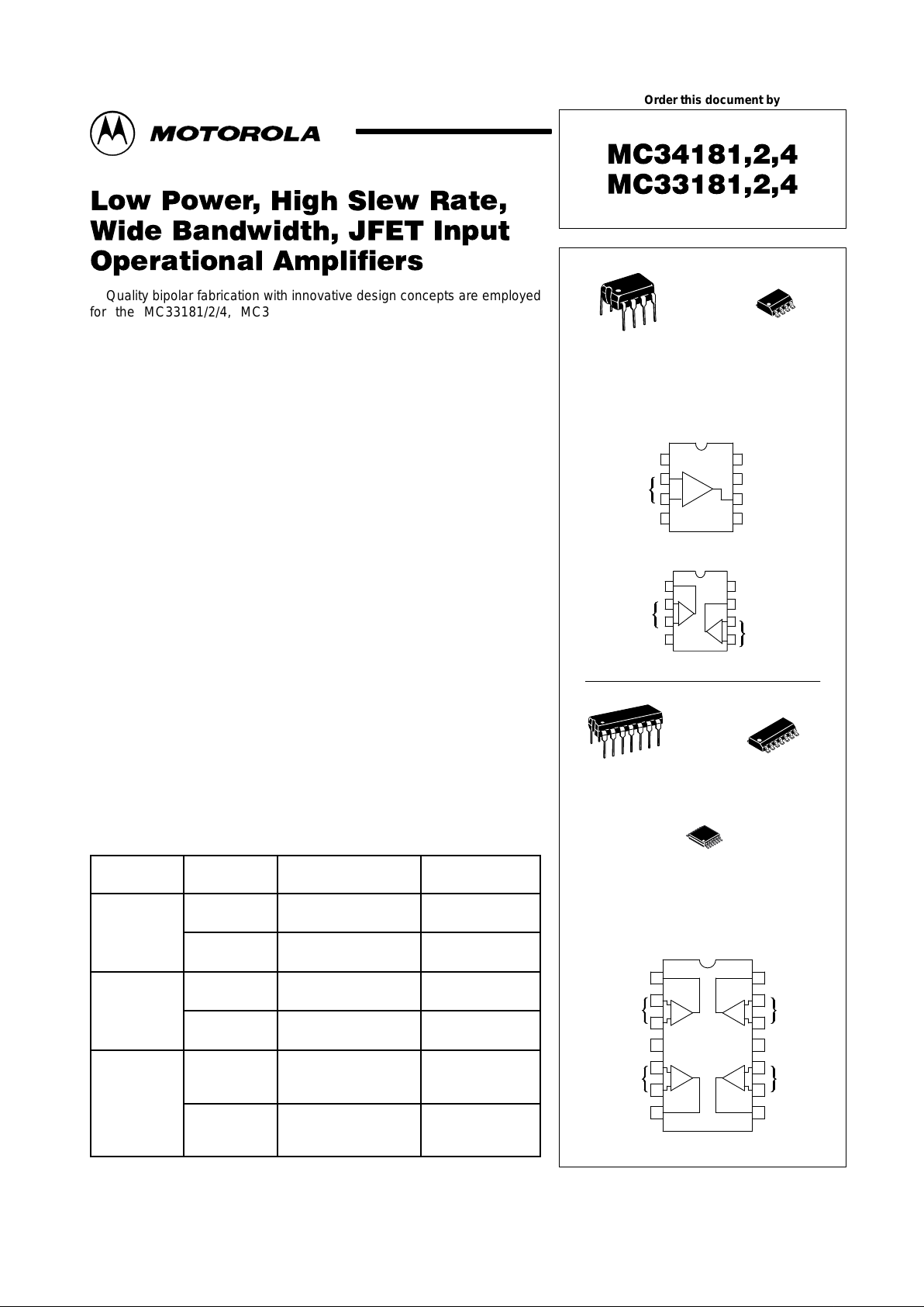
D SUFFIX
PLASTIC PACKAGE
CASE 751
(SO–8)
P SUFFIX
PLASTIC PACKAGE
CASE 626
P SUFFIX
PLASTIC PACKAGE
CASE 646
D SUFFIX
PLASTIC PACKAGE
CASE 751A
(SO–14)
PIN CONNECTIONS
(Single, Top View)
(Dual, Top View)
(Quad, Top View)
4
23
1
PIN CONNECTIONS
Offset Null
V
EE
V
EE
Inputs 1
Output 1
Inputs
NC
V
CC
Output
Offset Null
Inputs 2
Output 2
V
CC
1
2
3
4
8
7
6
5
+
1
2
3
4
8
7
6
5
1
2
1
2
3
4
5
6
78
9
10
11
12
13
14
Inputs 1
Output 1
V
CC
Inputs 2
Output 2
Output 4
Inputs 4
V
EE
Inputs 3
Output 3
–
+
–
+
–
+
–––
+
+
–
+
–
1
8
1
8
14
1
14
1
DTB SUFFIX
PLASTIC PACKAGE
CASE 948G
(TSSOP–14)
14
1
1
MOTOROLA ANALOG IC DEVICE DATA
"( "($ ( &
!(& !#'&
#$&"! #$%
Quality bipolar fabrication with innovative design concepts are employed
for the MC33181/2/4, MC34181/2/4 series of monolithic operational
amplifiers. This JFET input series of operational amplifiers operates at
210 µA per amplifier and offers 4.0 MHz of gain bandwidth product and
10 V/µs slew rate. Precision matching and an innovative trim technique of
the single and dual versions provide low input offset voltages. With a JFET
input stage, this series exhibits high input resistance, low input offset voltage
and high gain. The all NPN output stage, characterized by no deadband
crossover distortion and large output voltage swing, provides high
capacitance drive capability, excellent phase and gain margins, low open
loop high frequency output impedance and symmetrical source/sink AC
frequency response.
The MC33181/2/4, MC34181/2/4 series of devices are specified over the
commercial or industrial/vehicular temperature ranges. The complete series
of single, dual and quad operational amplifiers are available in the plastic
DIP as well as the SOIC surface mount packages.
• Low Supply Current: 210 µA (Per Amplifier)
• Wide Supply Operating Range: ±1.5 V to ±18 V
• Wide Bandwidth: 4.0 MHz
• High Slew Rate: 10 V/µs
• Low Input Offset Voltage: 2.0 mV
• Large Output Voltage Swing: –14 V to +14 V (with ±15 V Supplies)
• Large Capacitance Drive Capability: 0 pF to 500 pF
• Low Total Harmonic Distortion: 0.04%
• Excellent Phase Margin: 67°
• Excellent Gain Margin: 6.7 dB
• Output Short Circuit Protection
• Offered in New TSSOP Package Including the Standard SOIC and
DIP Packages
ORDERING INFORMATION
Op Amp
Function
Device
Operating
Temperature Range
Package
Single MC34181P
MC34181D
TA = 0° to +70°C
Plastic DIP
SO–8
MC33181P
MC33181D
TA = –40° to +85°C
Plastic DIP
SO–8
Dual MC34182P
MC34182D
TA = 0° to +70°C
Plastic DIP
SO–8
MC33182P
MC33182D
TA = –40° to +85°C
Plastic DIP
SO–8
Quad MC34184P
MC34184D
MC34184DTB
TA = 0° to +70°C
Plastic DIP
SO–14
TSSOP–14
MC33184P
MC33184D
MC33184DTB
TA = –40° to +85°C
Plastic DIP
SO–14
TSSOP–14
Motorola, Inc. 1996 Rev 1
MC34181,2,4 MC33181,2,4
2
MOTOROLA ANALOG IC DEVICE DATA
MAXIMUM RATINGS
Rating Symbol Value Unit
Supply Voltage (from VCC to VEE) V
S
+36 V
Input Differential Voltage Range V
IDR
Note 1 V
Input Voltage Range V
IR
Note 1 V
Output Short Circuit Duration (Note 2) t
SC
Indefinite sec
Operating Junction Temperature T
J
+150 °C
Storage Temperature Range T
stg
–60 to +150 °C
NOTES: 1. Either or both input voltages should not exceed the magnitude of VCC or VEE.
2.Power dissipation must be considered to ensure maximum junction temperature (TJ) is not
exceeded (see Figure 1).
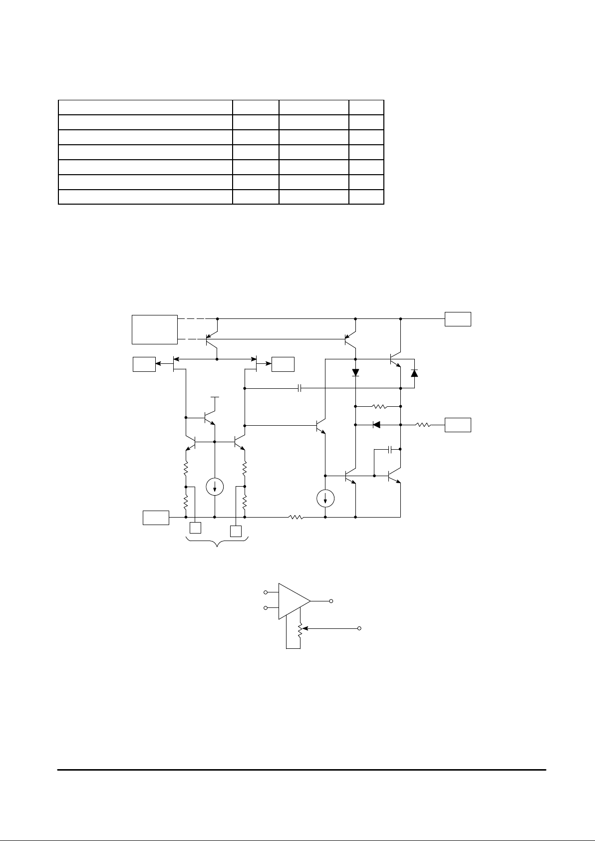
Q
8
Internal
Bias
Network
Neg Pos
V
CC
V
O
V
EE
J
1
J
2
Q
9
Q
7
D
3
D
1
C
1
R
6
D
2
R
7
C
2
Q
4
Q
6
Q
5
I
4
R
5
R
4
R
2
Q
3
I
3
R
3
R
1
Q
2
Q
1
Null Offsets
MC3X181 (Single) Only
1
5
1
5
V
EE
MC3X181 Input Offset
Voltage Null CIrcuit
25 k
Ω
–
+
+
Representative Schematic Diagram
(Each Amplifier)

MC34181,2,4 MC33181,2,4
3
MOTOROLA ANALOG IC DEVICE DATA
DC ELECTRICAL CHARACTERISTICS (V
CC
= +15 V , VEE = –15 V , TA = 25°C, unless otherwise noted.)
Characteristics Symbol Min Typ Max Unit
Input Offset Voltage (RS = 50 Ω, VO = 0 V)
Single
TA = +25°C
TA = 0° to +70°C (MC34181)
TA = –40° to +85°C (MC33181)
Dual
TA = +25°C
TA = 0° to +70°C (MC34182)
TA = –40° to +85°C (MC33182)
Quad
TA = +25°C
TA = 0° to +70°C (MC34184)
TA = –40° to +85°C (MC33184)
V
IO
—
—
—
—
—
—
—
—
—
0.5
—
—
1.0
—
—
4.0
—
—
2.0
3.0
3.5
3.0
4.0
4.5
10
11
11.5
mV
Average Temperature Coefficient of VIO (RS = 50 Ω, VO = 0V) ∆VIO/∆T — 10 — µV/°C
Input Offset Current (VCM = 0 V, VO = 0V)
TA = +25°C
TA = 0° to +70°C
TA = –40° to +85°C
I
IO
—
—
—
0.001
—
—
0.05
1.0
2.0
nA
Input Bias Current (VCM = 0 V, VO = 0V)
TA = +25°C
TA = 0° to +70°C
TA = –40° to +85°C
I
IB
—
—
—
0.003
—
—
0.1
2.0
4.0
nA
Input Common Mode Voltage Range V
ICR
(VEE +4.0 V) to (VCC –2.0 V) V
Large Signal Voltage Gain (RL = 10 kΩ, VO = ±10 V)
TA = +25°C
TA = T
low
to T
high
A
VOL
25
15
60
—
—
—
V/mV
Output Voltage Swing (VID = 1.0 V, RL = 10 kΩ)
TA = +25°C
VO+
VO–
+13.5
—
+14
–14
—
–13.5
V
Common Mode Rejection (RS = 50 Ω, VCM = V
ICR
, VO = 0 V) CMR 70 86 — dB
Power Supply Rejection (RS = 50 Ω, VCM = 0 V, VO = 0 V) PSR 70 84 — dB
Output Short Circuit Current (VID = 1.0 V , Output to Ground)
Source
Sink
I
SC
3.0
8.0
8.0
11
—
—
mA
Power Supply Current (No Load, VO = 0 V)
Single
TA = +25°C
TA = T
low
to T
high
Dual
TA = +25°C
TA = T
low
to T
high
Quad
TA = +25°C
TA = T
low
to T
high
I
D
—
—
—
—
—
—
210
—
420
—
840
—
250
250
500
500
1000
1000
µA
MC34181,2,4 MC33181,2,4
4
MOTOROLA ANALOG IC DEVICE DATA
AC ELECTRICAL CHARACTERISTICS
(VCC = +15 V , VEE = –15 V , TA = 25°C, unless otherwise noted.)
Characteristics Symbol Min Typ Max Unit
Slew Rate (Vin = –10 V to +10 V, RL = 10 kΩ, CL = 100 pF)
AV = +1.0
AV = –1.0
SR
7.0
—
10
10
—
—
V/µs
Settling Time (AV = –1.0, RL = 10 kΩ, VO = 0 V to +10 V Step)
To Within 0.10%
To Within 0.01%
t
s
—
—
1.1
1.5
—
—
µs
Gain Bandwidth Product (f = 100 kHz) GBW 3.0 4.0 — MHz
Power Bandwidth (AV = +1.0, RL = 10 kΩ, VO = 20 Vpp, THD = 5.0%) BW
p
— 120 — kHz
Phase Margin (–10 V < VO < +10 V)
RL = 10 kΩ
RL = 10 kΩ, CL = 100 pF
f
m
—
—
67
34
—
—
Degrees
Gain Margin (–10 V < VO < +10 V)
RL = 10 kΩ
RL = 10 kΩ, CL = 100 pF
A
m
—
—
6.7
3.4
—
—
dB
Equivalent Input Noise Voltage
RS = 100 Ω, f = 1.0 kHz
e
n
— 38 —
nV/ Hz√
Equivalent Input Noise Current
f = 1.0 kHz
i
n
— 0.01 —
pA/ Hz√
Differential Input Capacitance C
i
— 3.0 — pF
Differential Input Resistance R
i
— 10
12
— W
Total Harmonic Distortion
AV = 10, RL = 10 kΩ, 2.0 Vpp < VO < 20 Vpp, f = 1.0 kHz
THD — 0.04 — %
Channel Separation (RL = 10 kΩ, –10 V < VO < +10 V, 0 Hz < f < 10 kHz) — — 120 — dB
Open Loop Output Impedance
(f = 1.0 MHz)
|Zo| — 200 — Ω
8/14 Pin
Plastic
SO–8
SO–14
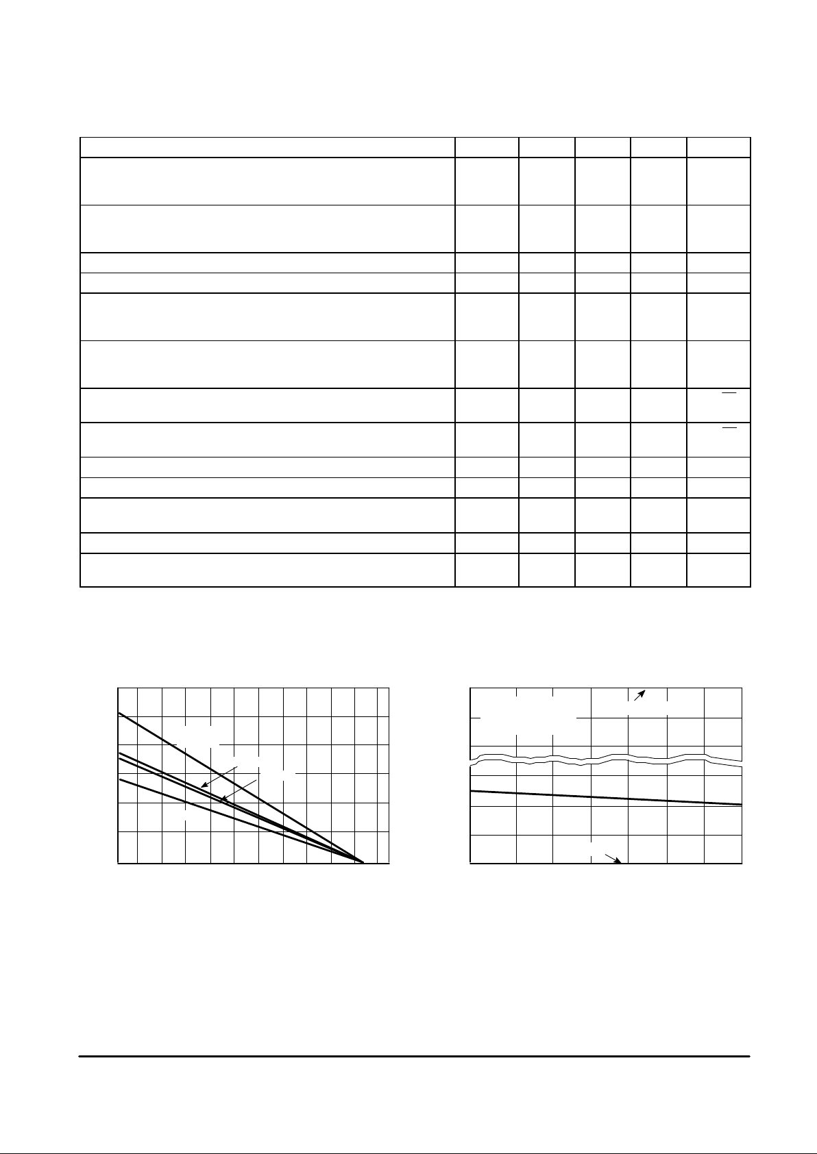
Figure 1. Maximum Power Dissipation versus
Temperature for Package Variations
Figure 2. Input Common Mode Voltage Range
versus Temperature
TA, AMBIENT TEMPERATURE (°C)
D
P , MAXIMUM POWER DISSIPATION (mW)
–55 –40 –20 0 20 40 60 80 100 120 140 160
TA, AMBIENT TEMPERATURE (°C)
ICR
V , INPUT COMMON MODE VOLTAGE
RANGE (V)
–55 –25 0 25 50 75 100 125
VCC = +3.0 V to +15 V
VEE = –3.0 V to –15 V
∆
VIO = 5.0 mV
VCC (VCM to VCC)
V
EE
2400
2000
1600
1200
800
400
0
0
–1.0
–2.0
3.0
2.0
1.0
0
TSSOP–14
 Loading...