

Motorola MC34167TH, MC34167TV, MC34167D2T, MC33167TH, MC33167TV Datasheet
...
Order this document by MC34167/D
The MC34167, MC33167 series are high performance fixed frequency
power switching regulators that contain the primary functions required for
dc–to–dc converters. This series was specifically designed to be
incorporated in step–down and voltage–inverting configurations with a
minimum number of external components and can also be used cost
effectively in step–up applications.
These devices consist of an internal temperature compensated
reference, fixed frequency oscillator with on–chip timing components,
latching pulse width modulator for single pulse metering, high gain error
amplifier, and a high current output switch.
Protective features consist of cycle–by–cycle current limiting,
undervoltage lockout, and thermal shutdown. Also included is a low power
standby mode that reduces power supply current to 36 µA.
• Output Switch Current in Excess of 5.0 A
• Fixed Frequency Oscillator (72 kHz) with On–Chip Timing
• Provides 5.05 V Output without External Resistor Divider
• Precision 2% Reference
• 0% to 95% Output Duty Cycle
• Cycle–by–Cycle Current Limiting
• Undervoltage Lockout with Hysteresis
• Internal Thermal Shutdown
• Operation from 7.5 V to 40 V
• Standby Mode Reduces Power Supply Current to 36 µA
• Economical 5–Lead TO–220 Package with Two Optional Leadforms
• Also Available in Surface Mount D
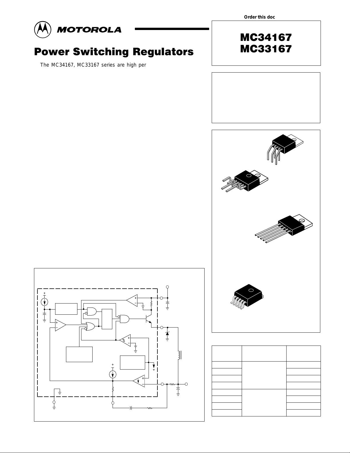
Simplified Block Diagram
(Step Down Application)
Oscillator
PWM
Thermal
3
This device contains 143 active transistors.
2
PAK Package
V
in
I
LIMIT
S
Q
R
UVLO
Reference
EA
5
4
2
L
1
V
O
5.05 V/5.0 A
POWER SWITCHING
REGULATORS
SEMICONDUCTOR
TECHNICAL DATA
TH SUFFIX
PLASTIC PACKAGE
CASE 314A
1
5
1
5
Heatsink surface connected to Pin 3.
T SUFFIX
PLASTIC PACKAGE
CASE 314D
1
Pin 1. V oltage Feedback Input
2. Switch Output
3. Ground
4. Input V oltage/V
5. Compensation/Standby
1
5
Heatsink surface (shown as terminal 6
in case outline drawing) is connected to Pin 3.
ORDERING INFORMATION
Operating
Device
MC33167D2T
MC33167T
MC33167TH
MC33167TV
MC34167D2T
MC34167T
MC34167TH
MC34167TV
Temperature Range
TA = –40° to +85°C
TA = 0° to + 70°C
TV SUFFIX
PLASTIC PACKAGE
CASE 314B
5
CC
D2T SUFFIX
PLASTIC PACKAGE
CASE 936A
(D2PAK)
Package
Surface Mount
Straight Lead
Horiz. Mount
Vertical Mount
Surface Mount
Straight Lead
Horiz. Mount
Vertical Mount
MOTOROLA ANALOG IC DEVICE DATA
Motorola, Inc. 1996 Rev 3
1
MAXIMUM RATINGS
Rating Symbol Value Unit
Power Supply Input Voltage V
Switch Output Voltage Range V
Voltage Feedback and Compensation Input
Voltage Range
Power Dissipation
Case 314A, 314B and 314D (TA = +25°C) P
Thermal Resistance, Junction–to–Ambient θ
Thermal Resistance, Junction–to–Case θ
Case 936A (D2PAK) (TA = +25°C) P
Thermal Resistance, Junction–to–Ambient θ
Thermal Resistance, Junction–to–Case θ
Operating Junction Temperature T
Operating Ambient Temperature (Note 3)
MC34167
MC33167
Storage Temperature Range T
V
FB, VComp
MC34167 MC33167
CC
O(switch)
D
JA
JC
D
JA
JC
J
T
A
stg
40 V
–2.0 to + V
in
–1.0 to + 7.0 V
Internally Limited W
65 °C/W
5.0 °C/W
Internally Limited W
70 °C/W
5.0 °C/W
+150 °C
0 to + 70
– 40 to + 85
– 65 to +150 °C
V
°C
ELECTRICAL CHARACTERISTICS (V
= 12 V, for typical values TA = +25°C, for min/max values TA is the operating ambient
CC
temperature range that applies [Notes 2, 3], unless otherwise noted.)
Characteristic
Symbol Min Typ Max Unit
OSCILLAT OR
Frequency (VCC = 7.5 V to 40 V) TA = +25°C
TA = T
low
to T
high
f
OSC
65
62
72
–
81
79
ERROR AMPLIFIER
Voltage Feedback Input Threshold TA =+ 25°C
TA = T
low
to T
high
Line Regulation (VCC = 7.5 V to 40 V, TA = +25°C) Reg
Input Bias Current (VFB = V
+ 0.15 V) I
FB(th)
V
FB(th)
IB
line
4.95
4.85
5.05
–
5.15
5.20
– 0.03 0.078 %/V
– 0.15 1.0 µA
Power Supply Rejection Ratio (VCC = 10 V to 20 V, f = 120 Hz) PSRR 60 80 – dB
Output Voltage Swing High State (I
Low State (I
= 75 µA, VFB = 4.5 V)
Source
= 0.4 mA, VFB = 5.5 V)
Sink
V
OH
V
OL
4.2
–
1.6
4.9
–
1.9
PWM COMPARATOR
Duty Cycle (VCC = 20 V) Maximum (VFB = 0 V)
Minimum (V
Comp
= 1.9 V)
DC
DC
(max)
(min)
92
0
0
95
100
0
SWITCH OUTPUT
Output Voltage Source Saturation (VCC = 7.5 V, I
Off–State Leakage (VCC = 40 V, Pin 2 = Gnd) I
Current Limit Threshold (VCC = 7.5 V) I
= 5.0 A) V
Source
sat
sw(off)
pk(switch)
– (VCC –1.5) (VCC –1.8) V
– 0 100 µA
5.5 6.5 8.0 A
Switching Times (VCC = 40 V, Ipk = 5.0 A, L = 225 µH, TA = +25°C)
Output Voltage Rise T ime
Output Voltage Fall T ime
t
r
t
f
–
–
100
50
200
100
UNDERVOLTAGE LOCKOUT
Startup Threshold (VCC Increasing, TA = +25°C) V
Hysteresis (VCC Decreasing, TA = +25°C) V
th(UVLO)
H(UVLO)
5.5 5.9 6.3 V
0.6 0.9 1.2 V
TOTAL DEVICE
Power Supply Current (TA = +25°C )
Standby (VCC = 12 V, V
Operating (VCC = 40 V, Pin 1 = Gnd for maximum duty cycle)
NOTES: 1.Maximum package power dissipation limits must be observed to prevent thermal shutdown activation.
2.Low duty cycle pulse techniques are used during test to maintain junction temperature as close to ambient as possible.
3.T
=0°C for MC34167 T
low
=–40°C for MC33167 = +85°C for MC33167
Comp
< 0.15 V)
high
= + 70°C for MC34167
I
CC
–
–
36
40
100
60
kHz
V
V
%
ns
µA
mA
2
MOTOROLA ANALOG IC DEVICE DATA
MC34167 MC33167
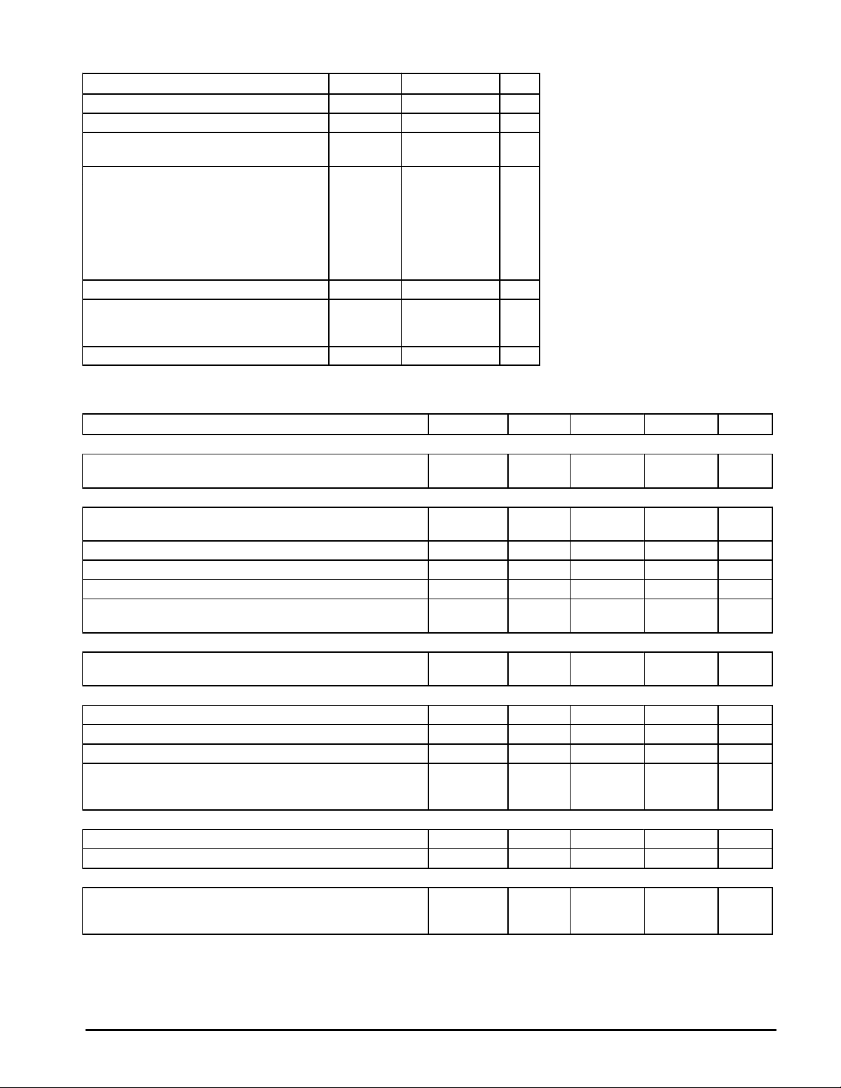
Figure 1. V oltage Feedback Input Threshold
versus T emperature
5.25
VCC = 12 V
5.17
5.09
5.01
4.93
, VOLTAGE FEEDBACK INPUT THRESHOLD (V)
4.85
– 55 – 25 0 25 50 75 100 125
FB(th)
V
TA, AMBIENT TEMPERATURE (°C)
V
FB(th)
V
V
FB(th)
FB(th)
Max = 5.15 V
Typ = 5.05 V
Min = 4.95 V
Figure 3. Error Amp Open Loop Gain and
Phase versus Frequency
100
80
60
40
20
, OPEN LOOP VOL TAGE GAIN (dB)
0
VOL
A
–20
Gain
100 1.0 k 10 k 100 k 1.0 M
f, FREQUENCY (Hz)
VCC = 12 V
V
= 3.25 V
Comp
RL = 100 k
TA = +25
Phase
°
C
100
80
60
40
, INPUT BIAS CURRENT (nA)
20
IB
I
0
– 55 – 25 0 25 50 75 100 125
0
30
60
90
120
150
180
10 M10
2.0
1.6
1.2
0.8
0.4
, EXCESS PHASE (DEGREES)
φ
, OUTPUT SA TURATION VOLTAGE (V)
sat
V
0
Figure 2. V oltage Feedback Input Bias
Current versus Temperature
VCC = 12 V
VFB = V
FB(th)
TA, AMBIENT TEMPERATURE (°C)
Figure 4. Error Amp Output Saturation
versus Sink Current
VCC = 12 V
VFB = 5.5 V
TA = +25
0.4 0.8 1.2 1.6
I
, OUTPUT SINK CURRENT (mA)
Sink
°
C
2.00
Figure 5. Oscillator Frequency Change
versus T emperature
4.0
0
– 4.0
– 8.0
, OSCILLAT OR FREQUENCY CHANGE (%)
OSC
–12
f
–55
∆
– 25 0 25 50 75 100 125
TA, AMBIENT TEMPERATURE (
MOTOROLA ANALOG IC DEVICE DATA
VCC = 12 V
°
C)
100
80
60
40
20
DC, SWITCH OUTPUT DUTY CYCLE (%)
0
1.5
Figure 6. Switch Output Duty Cycle
versus Compensation V oltage
VCC = 12 V
°
TA = +25
C
2.0 2.5 3.0 3.5 4.0
V
, COMPENSATION VOLTAGE (V)
Comp
4.5
3
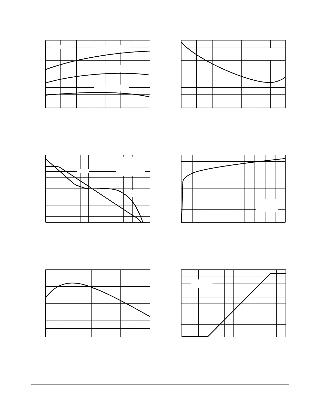
MC34167 MC33167
Figure 7. Switch Output Source Saturation
versus Source Current
0
V
CC
– 0.5
–1.0
–1.5
– 2.0
– 2.5
, SWITCH OUTPUT SOURCE SA TURATION (V)
– 3.0
sat
V
0 2.0 4.0 6.0 8.0
I
, SWITCH OUTPUT SOURCE CURRENT (A)
Source
TA = +25°C
Figure 9. Switch Output Current Limit
Threshold versus T emperature
7.2
VCC = 12 V
Pins 1, 2, 3 = Gnd
6.8
Figure 8. Negative Switch Output Voltage
versus T emperature
0
Gnd
– 0.2
VCC = 12 V
Pin 5 = 2.0 V
– 0.4
Pins 1, 3 = Gnd
Pin 2 Driven Negative
– 0.6
– 0.8
, SWITCH OUTPUT VOL TAGE (V)
–1.0
sw
V
–1.2
– 55 – 25 0 25 50 75 100 125
Isw = 10 mA
TA, AMBIENT TEMPERATURE (°C)
Isw = 100 µA
Figure 10. Standby Supply Current
versus Supply V oltage
160
Pin 4 = V
CC
Pins 1, 3, 5 = Gnd
A)
µ
120
Pin 2 Open
°
C
TA = +25
6.4
6.0
, CURRENT LIMIT THRESHOLD (A)
pk(switch)
5.6
I
– 55 – 25 0 25 50 75 100 125
TA, AMBIENT TEMPERATURE (
°
C)
Figure 11. Undervoltage Lockout
Thresholds versus T emperature
6.5
6.0
5.5
5.0
4.5
, UNDERVOL TAGE LOCKOUT THRESHOLD (V)
4.0
–55
th(UVLO)
V
– 25 0 25 50 75 100 125
TA, AMBIENT TEMPERATURE (
Startup Threshold
VCC Increasing
Turn–Off Threshold
VCC Decreasing
°
C)
, SUPPLY CURRENT (
CC
I
, SUPPLY CURRENT (mA)
CC
I
80
40
50
40
30
20
10
0
0
10 20 30 40
VCC, SUPPLY VOLTAGE (V)
Figure 12. Operating Supply Current
versus Supply V oltage
0
0
10 20 30
VCC, SUPPLY VOLTAGE (V)
Pin 4 = V
CC
Pins 1, 3 = Gnd
Pins 2, 5 Open
°
C
TA = +25
40
4
MOTOROLA ANALOG IC DEVICE DATA
MC34167 MC33167
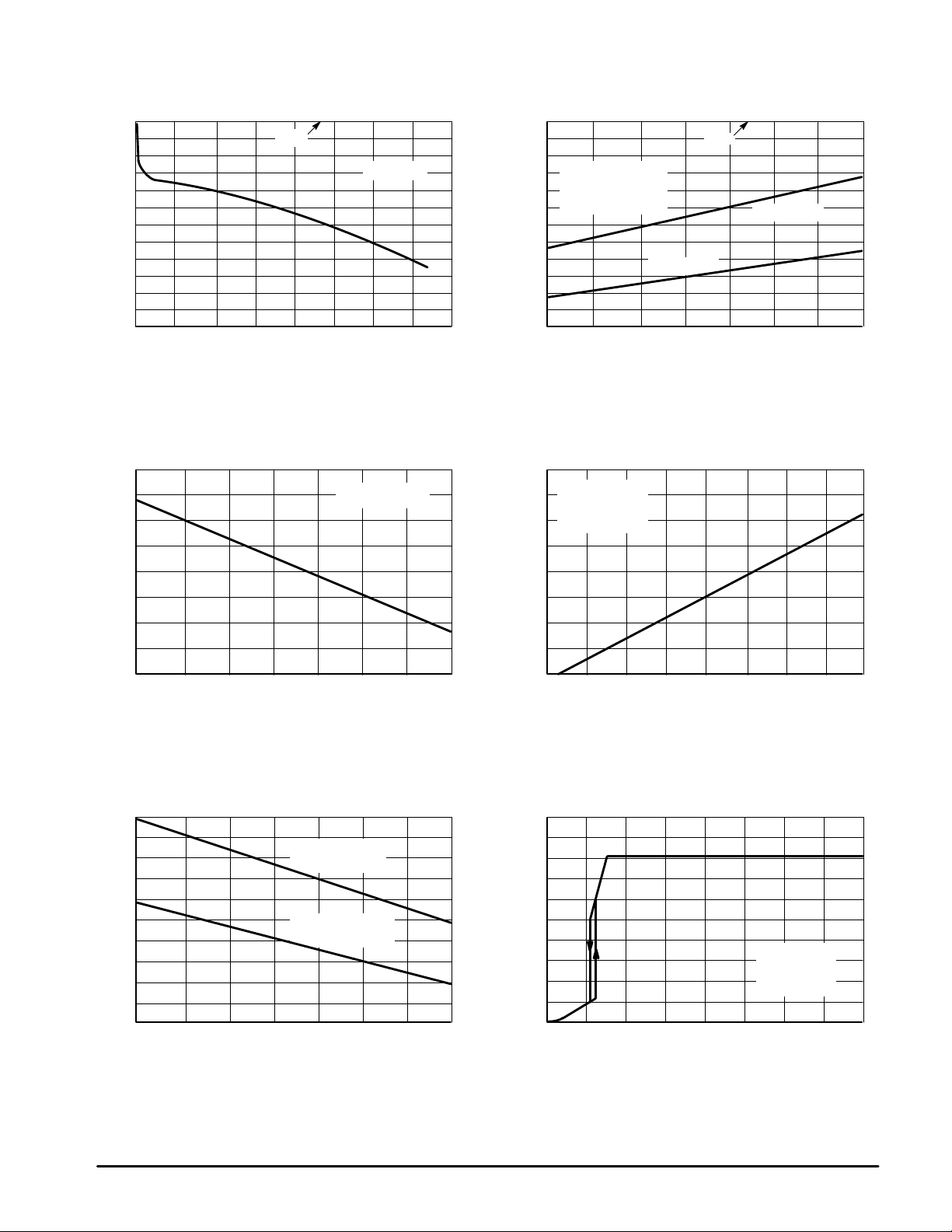
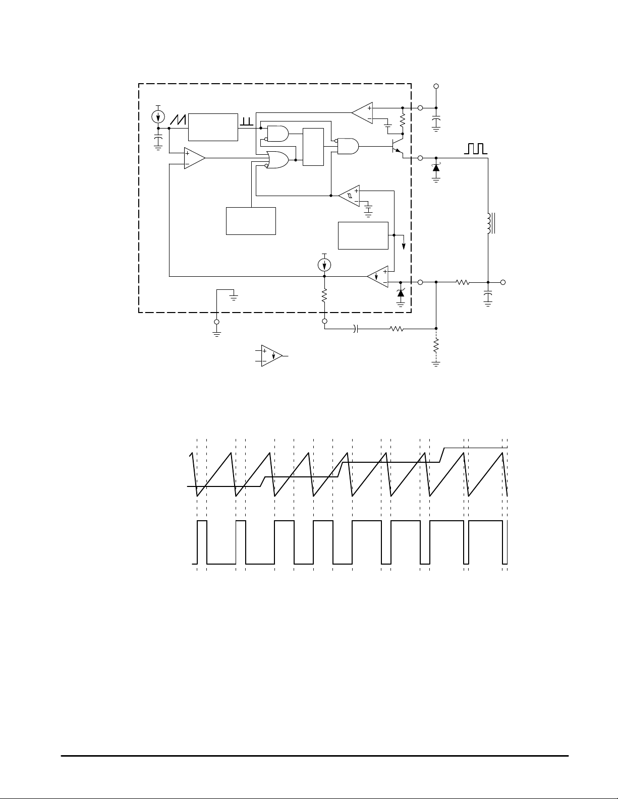
Figure 13. MC34167 Representative Block Diagram
V
in
+
C
T
Oscillator
Pulse Width
Modulator
PWM Latch
Current
Sense
S
Q
R
Undervoltage
Lockout
4
Switch
Output
2
Input Voltage/V
C
in
CC
4.1 V
Timing Capacitor C
Compensation
T
2.3 V
Thermal
Shutdown
100
µ
A
Gnd Compensation
3
Sink Only
=
Positive True Logic
Figure 14. Timing Diagram
+
120
5
5.05 V
Reference
Error
Amp
C
F
R
F
Voltage
+
Feedback
Input
L
V
1
R
2
R
1
O
C
O
ON
Switch Output
OFF
MOTOROLA ANALOG IC DEVICE DATA
5
 Loading...