

The MC34166, MC33166 series are high performance fixed frequency
power switching regulators that contain the primary functions required for
dc–to–dc converters. This series was specifically designed to be
incorporated in step–down and voltage–inverting configurations with a
minimum number of external components and can also be used cost
effectively in step–up applications.
These devices consist of an internal temperature compensated
reference, fixed frequency oscillator with on–chip timing components,
latching pulse width modulator for single pulse metering, high gain error
amplifier, and a high current output switch.
Protective features consist of cycle–by–cycle current limiting,
undervoltage lockout, and thermal shutdown. Also included is a low power
standby mode that reduces power supply current to 36 µA.
• Output Switch Current in Excess of 3.0 A
• Fixed Frequency Oscillator (72 kHz) with On–Chip Timing
• Provides 5.05 V Output without External Resistor Divider
• Precision 2% Reference
• 0% to 95% Output Duty Cycle
• Cycle–by–Cycle Current Limiting
• Undervoltage Lockout with Hysteresis
• Internal Thermal Shutdown
• Operation from 7.5 V to 40 V
• Standby Mode Reduces Power Supply Current to 36 µA
• Economical 5–Lead TO–220 Package with Two Optional Leadforms
• Also Available in Surface Mount D
2
PAK Package
Order this document by MC34166/D
POWER SWITCHING
REGULATORS
SEMICONDUCTOR
TECHNICAL DATA
TH SUFFIX
PLASTIC PACKAGE
CASE 314A
1
5
Heatsink surface connected to Pin 3.
T SUFFIX
PLASTIC PACKAGE
CASE 314D
1
5
1
5
TV SUFFIX
PLASTIC PACKAGE
CASE 314B
3
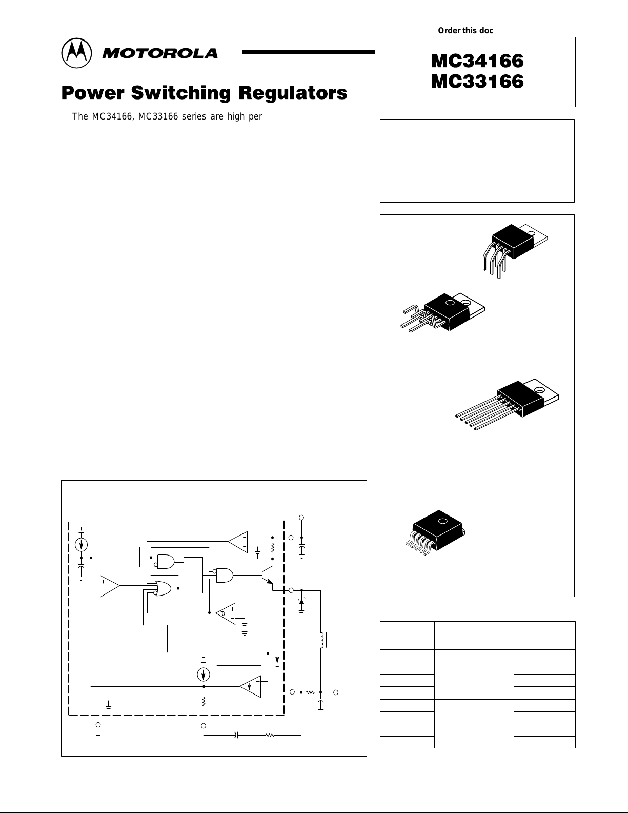
Oscillator
PWM
Simplified Block Diagram
(Step Down Application)
I
LIMIT
S
Q
R
UVLO
Thermal
Reference
EA
5
This device contains 143 active transistors.
Pin 1. V oltage Feedback Input
2. Switch Output
3. Ground
4. Input V oltage/V
5. Compensation/Standby
V
in
4
1
5
Heatsink surface (shown as terminal 6
2
in case outline drawing) is connected to Pin 3.
CC
D2T SUFFIX
PLASTIC PACKAGE
CASE 936A
(D2PAK)
ORDERING INFORMATION
L
1
V
O
5.05 V/3.0 A
Device
MC33166D2T
MC33166T
MC33166TH
MC33166TV
MC34166D2T
MC34166T
MC34166TH
MC34166TV
Operating
Temperature Range
TA = – 40° to + 85°C
TA = 0° to + 70°C
Package
Surface Mount
Straight Lead
Horiz. Mount
Vertical Mount
Surface Mount
Straight Lead
Horiz. Mount
Vertical Mount
MOTOROLA ANALOG IC DEVICE DATA
Motorola, Inc. 1996 Rev 4
1
MAXIMUM RATINGS
Rating Symbol Value Unit
Power Supply Input Voltage V
Switch Output Voltage Range V
Voltage Feedback and Compensation Input
Voltage Range
Power Dissipation
Case 314A, 314B and 314D (TA = +25°C) P
Thermal Resistance, Junction–to–Ambient θ
Thermal Resistance, Junction–to–Case θ
Case 936A (D2PAK) (TA = +25°C) P
Thermal Resistance, Junction–to–Ambient θ
Thermal Resistance, Junction–to–Case θ
Operating Junction Temperature T
Operating Ambient Temperature (Note 3)
MC34166
MC33166
Storage Temperature Range T
V
FB, VComp
MC34166 MC33166
CC
O(switch)
D
JA
JC
D
JA
JC
J
T
A
stg
40 V
–1.5 to + V
in
–1.0 to + 7.0 V
Internally Limited W
65 °C/W
5.0 °C/W
Internally Limited W
70 °C/W
5.0 °C/W
+150 °C
0 to + 70
– 40 to + 85
– 65 to +150 °C
V
°C
ELECTRICAL CHARACTERISTICS (V
= 12 V, for typical values TA = +25°C, for min/max values TA is the operating ambient
CC
temperature range that applies [Notes 2, 3], unless otherwise noted.)
Characteristic
Symbol Min Typ Max Unit
OSCILLAT OR
Frequency (VCC = 7.5 V to 40 V) TA = +25°C
TA = T
low
to T
high
f
OSC
65
62
72
–
81
79
ERROR AMPLIFIER
Voltage Feedback Input Threshold TA = +25°C
TA = T
low
to T
high
Line Regulation (VCC = 7.5 V to 40 V, TA = +25°C) Reg
Input Bias Current (VFB = V
+ 0.15 V) I
FB(th)
V
FB(th)
IB
line
4.95
4.85
5.05
–
5.15
5.2
– 0.03 0.078 %/V
– 0.15 1.0 µA
Power Supply Rejection Ratio (VCC = 10 V to 20 V, f = 120 Hz) PSRR 60 80 – dB
Output Voltage Swing
High State (I
Low State (I
= 75 µA, VFB = 4.5 V)
Source
= 0.4 mA, VFB = 5.5 V)
Sink
V
OH
V
OL
4.2
–
4.9
1.6
–
1.9
PWM COMPARATOR
Duty Cycle
Maximum (VFB = 0 V)
Minimum (V
Comp
= 1.9 V)
DC
DC
(max)
(min)
92
0
0
95
100
0
SWITCH OUTPUT
Output Voltage Source Saturation (VCC = 7.5 V, I
Off–State Leakage (VCC = 40 V, Pin 2 = Gnd) I
Current Limit Threshold I
= 3.0 A) V
Source
sat
sw(off)
pk(switch)
– (V
CC
–1.5)
(V
CC
–1.8)
– 0 100 µA
3.3 4.3 6.0 A
Switching Times (VCC = 40 V, Ipk = 3.0 A, L = 375 µH, TA = +25°C)
Output Voltage Rise T ime
Output Voltage Fall T ime
t
r
t
f
–
–
100
50
200
100
UNDERVOLTAGE LOCKOUT
Startup Threshold (VCC Increasing, TA = +25°C) V
Hysteresis (VCC Decreasing, TA = +25°C) V
th(UVLO)
H(UVLO)
5.5 5.9 6.3 V
0.6 0.9 1.2 V
TOTAL DEVICE
Power Supply Current (TA = +25°C )
Standby (VCC = 12 V, V
Operating (VCC = 40 V, Pin 1 = Gnd for maximum duty cycle)
NOTES: 1. Maximum package power dissipation limits must be observed to prevent thermal shutdown activation.
2.Low duty cycle pulse techniques are used during test to maintain junction temperature as close to ambient as possible.
3.T
=0°C for MC34166 T
low
=–40°C for MC33166 = + 85°C for MC33166
Comp
< 0.15 V)
high
= + 70°C for MC34166
I
CC
–
–
36
31
100
55
kHz
V
V
%
V
ns
µA
mA
2
MOTOROLA ANALOG IC DEVICE DATA
MC34166 MC33166
Figure 1. V oltage Feedback Input Threshold
versus T emperature
5.25
VCC = 12 V
5.17
5.09
5.01
4.93
, VOLTAGE FEEDBACK INPUT THRESHOLD (V)
4.85
– 55 – 25 0 25 50 75 100 125
FB(th)
V
TA, AMBIENT TEMPERATURE (°C)
V
FB(th)
V
FB(th)
V
FB(th)
Max = 5.15 V
Typ = 5.05 V
Min = 4.95 V
Figure 3. Error Amp Open Loop Gain and
Phase versus Frequency
100
80
60
40
20
, OPEN LOOP VOL TAGE GAIN (dB)
0
VOL
A
–20
Gain
100 1.0 k 10 k 100 k 1.0 M
f, FREQUENCY (Hz)
VCC = 12 V
V
= 3.25 V
Comp
RL = 100 k
TA = +25
°
C
Phase
100
80
60
40
, INPUT BIAS CURRENT (nA)
20
IB
I
0
– 55 – 25 0 25 50 75 100 125
0
30
60
90
120
150
180
10 M10
2.0
1.6
1.2
0.8
0.4
, EXCESS PHASE (DEGREES)
φ
, OUTPUT SA TURATION VOLTAGE (V)
sat
V
0
Figure 2. V oltage Feedback Input Bias
Current versus Temperature
VCC = 12 V
VFB = V
FB(th)
TA, AMBIENT TEMPERATURE (°C)
Figure 4. Error Amp Output Saturation
versus Sink Current
VCC = 12 V
VFB = 5.5 V
°
C
TA = +25
0.4 0.8 1.2 1.6
I
, OUTPUT SINK CURRENT (mA)
Sink
2.00
Figure 5. Oscillator Frequency Change
versus T emperature
4.0
0
– 4.0
– 8.0
, OSCILLAT OR FREQUENCY CHANGE (%)
OSC
–12
f
–55
∆
– 25 0 25 50 75 100 125
TA, AMBIENT TEMPERATURE (
MOTOROLA ANALOG IC DEVICE DATA
VCC = 12 V
°
C)
100
80
60
40
20
DC, SWITCH OUTPUT DUTY CYCLE (%)
0
1.5
Figure 6. Switch Output Duty Cycle
versus Compensation V oltage
VCC = 12 V
°
C
TA = +25
2.0 2.5 3.0 3.5 4.0
V
, COMPENSATION VOLTAGE (V)
Comp
4.5
3
MC34166 MC33166
Figure 7. Switch Output Source Saturation
versus Source Current
0
V
– 0.5
–1.0
–1.5
– 2.0
– 2.5
, SWITCH OUTPUT SOURCE SA TURATION (V)
– 3.0
sat
0 2.0 3.0 4.0 5.0
V
1.0
I
, SWITCH OUTPUT SOURCE CURRENT (A)
Source
CC
TA = +25°C
Figure 9. Switch Output Current Limit
Threshold versus T emperature
4.7
VCC = 12 V
Pins 1, 2, 3 = Gnd
4.5
Figure 8. Negative Switch Output Voltage
versus T emperature
0
VCC = 12 V
– 0.2
Pin 5 = 2.0 V
Pins 1, 3 = Gnd
– 0.4
Pin 2 Driven Negative
– 0.6
– 0.8
–1.0
, SWITCH OUTPUT VOL TAGE (V)
sw
V
–1.2
– 55 – 25 0 25 50 75 100 125
Isw = 10 mA
TA, AMBIENT TEMPERATURE (°C)
Gnd
Isw = 100 µA
Figure 10. Standby Supply Current
versus Supply V oltage
160
Pin 4 = V
CC
Pins 1, 3, 5 = Gnd
A)
µ
120
Pin 2 Open
°
C
TA = +25
4.3
4.1
, CURRENT LIMIT THRESHOLD (A)
pk(switch)
3.9
I
– 55 – 25 0 25 50 75 100 125
TA, AMBIENT TEMPERATURE (°C)
Figure 11. Undervoltage Lockout
Threshold versus T emperature
6.5
6.0
5.5
5.0
4.5
, UNDERVOL TAGE LOCKOUT THRESHOLD (V)
4.0
–55
th(UVLO)
V
– 25 0 25 50 75 100 125
TA, AMBIENT TEMPERATURE (
Startup Threshold
VCC Increasing
Turn–Off Threshold
VCC Decreasing
°
C)
, SUPPLY CURRENT (
CC
I
, SUPPLY CURRENT (mA)
CC
I
40
30
20
10
80
40
0
0
10 20 30 40
VCC, SUPPLY VOLTAGE (V)
Figure 12. Operating Supply Current
versus Supply V oltage
0
0
10 20 30
VCC, SUPPLY VOLTAGE (V)
Pin 4 = V
CC
Pins 1, 3 = Gnd
Pins 2, 5 Open
°
C
TA = +25
40
4
MOTOROLA ANALOG IC DEVICE DATA
MC34166 MC33166
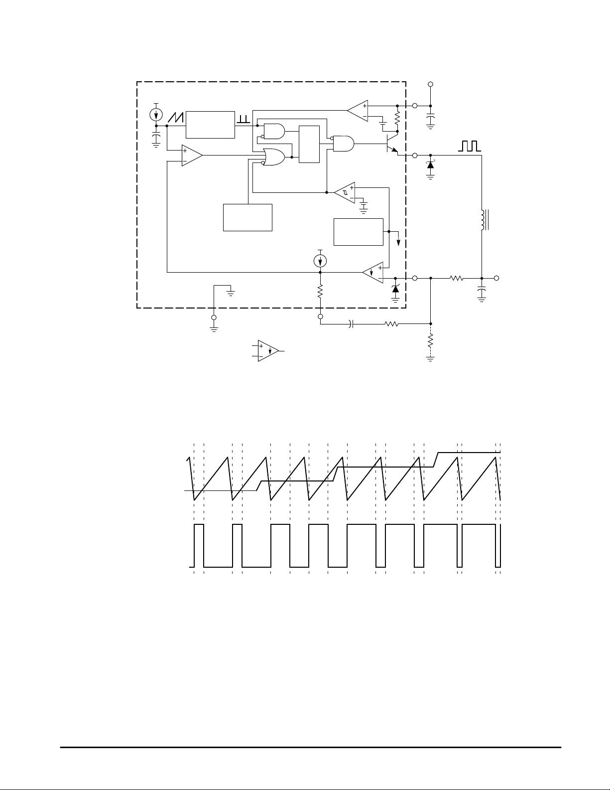
Figure 13. MC34166 Representative Block Diagram
V
in
+
C
T
Oscillator
Pulse Width
Modulator
PWM Latch
Current
Sense
S
Q
R
Undervoltage
Lockout
4
Switch
Output
2
Input Voltage/V
C
in
CC
Timing Capacitor C
4.1 V
T
Compensation
2.3 V
Thermal
Shutdown
µ
A
100
Gnd Compensation
3
Sink Only
=
Positive True Logic
Figure 14. Timing Diagram
+
120
5
5.05 V
Reference
Error
Amp
C
F
R
F
Voltage
+
Feedback
Input
L
V
1
R
2
R
1
O
C
O
ON
Switch Output
OFF
MOTOROLA ANALOG IC DEVICE DATA
5

MC34166 MC33166
INTRODUCTION
The MC34166, MC33166 series are monolithic power
switching regulators that are optimized for dc–to–dc converter
applications. These devices operate as fixed frequency,
voltage mode regulators containing all the active functions
required to directly implement step–down and
voltage–inverting converters with a minimum number of
external components. They can also be used cost effectively
in step–up converter applications. Potential markets include
automotive, computer, industrial, and cost sensitive consumer
products. A description of each section of the device is given
below with the representative block diagram shown in
Figure 13.
Oscillator
The oscillator frequency is internally programmed to
72 kHz by capacitor CT and a trimmed current source. The
charge to discharge ratio is controlled to yield a 95%
maximum duty cycle at the Switch Output. During the
discharge of CT, the oscillator generates an internal blanking
pulse that holds the inverting input of the AND gate high,
disabling the output switch transistor. The nominal oscillator
peak and valley thresholds are 4.1 V and 2.3 V respectively .
Pulse Width Modulator
The Pulse Width Modulator consists of a comparator with
the oscillator ramp voltage applied to the noninverting input,
while the error amplifier output is applied into the inverting
input. Output switch conduction is initiated when CT is
discharged to the oscillator valley voltage. As CT charges to
a voltage that exceeds the error amplifier output, the latch
resets, terminating output transistor conduction for the
duration of the oscillator ramp–up period. This PWM/Latch
combination prevents multiple output pulses during a given
oscillator clock cycle. Figures 6 and 14 illustrate the switch
output duty cycle versus the compensation voltage.
Current Sense
The MC34166 series utilizes cycle–by–cycle current
limiting as a means of protecting the output switch transistor
from overstress. Each on–cycle is treated as a separate
situation. Current limiting is implemented by monitoring the
output switch transistor current buildup during conduction, and
upon sensing an overcurrent condition, immediately turning off
the switch for the duration of the oscillator ramp–up period.
The collector current is converted to a voltage by an
internal trimmed resistor and compared against a reference
by the Current Sense comparator. When the current limit
threshold is reached, the comparator resets the PWM latch.
The current limit threshold is typically set at 4.3 A. Figure 9
illustrates switch output current limit threshold versus
temperature.
Error Amplifier and Reference
A high gain Error Amplifier is provided with access to the
inverting input and output. This amplifier features a typical dc
voltage gain of 80 dB, and a unity gain bandwidth of
600 kHz with 70 degrees of phase margin (Figure 3). The
noninverting input is biased to the internal 5.05 V reference
and is not pinned out. The reference has an accuracy of
± 2.0% at room temperature. T o provide 5.0 V at the load, the
reference is programmed 50 mV above 5.0 V to compensate
for a 1.0% voltage drop in the cable and connector from the
converter output. If the converter design requires an output
voltage greater than 5.05 V, resistor R1 must be added to
form a divider network at the feedback input as shown in
Figures 13 and 18. The equation for determining the output
voltage with the divider network is:
R
2
V
+
out
External loop compensation is required for converter
stability. A simple low–pass filter is formed by connecting a
resistor (R2) from the regulated output to the inverting input,
and a series resistor–capacitor (RF, CF) between Pins 1 and
5. The compensation network component values shown in
each of the applications circuits were selected to provide
stability over the tested operating conditions. The step–down
converter (Figure 18) is the easiest to compensate for
stability. The step–up (Figure 20) and voltage–inverting
(Figure 22) configurations operate as continuous conduction
flyback converters, and are more difficult to compensate. The
simplest way to optimize the compensation network is to
observe the response of the output voltage to a step load
change, while adjusting RF and CF for critical damping. The
final circuit should be verified for stability under four boundary
conditions. These conditions are minimum and maximum
input voltages, with minimum and maximum loads.
By clamping the voltage on the error amplifier output
(Pin 5) to less than 150 mV, the internal circuitry will be
placed into a low power standby mode, reducing the power
supply current to 36 µA with a 12 V supply voltage. Figure 10
illustrates the standby supply current versus supply voltage.
The Error Amplifier output has a 100 µA current source
pull–up that can be used to implement soft–start. Figure 17
shows the current source charging capacitor CSS through a
series diode. The diode disconnects CSS from the feedback
loop when the 1.0 M resistor charges it above the operating
range of Pin 5.
Switch Output
The output transistor is designed to switch a maximum of
40 V, with a minimum peak collector current of 3.3 A. When
configured for step–down or voltage–inverting applications,
as in Figures 18 and 22, the inductor will forward bias the
output rectifier when the switch turns off. Rectifiers with a
high forward voltage drop or long turn–on delay time should
not be used. If the emitter is allowed to go sufficiently
negative, collector current will flow, causing additional device
heating and reduced conversion efficiency. Figure 8 shows
that by clamping the emitter to 0.5 V , the collector current will
be in the range of 100 µA over temperature. A 1N5822 or
equivalent Schottky barrier rectifier is recommended to fulfill
these requirements.
Undervoltage Lockout
An Undervoltage Lockout comparator has been
incorporated to guarantee that the integrated circuit is fully
functional before the output stage is enabled. The internal
5.05 V reference is monitored by the comparator which
enables the output stage when VCC exceeds 5.9 V. To
prevent erratic output switching as the threshold is crossed,
0.9 V of hysteresis is provided.
5.05
ǒ
Ǔ
)
1
R
1
6
MOTOROLA ANALOG IC DEVICE DATA

MC34166 MC33166
Thermal Protection
Internal Thermal Shutdown circuitry is provided to protect
the integrated circuit in the event that the maximum junction
temperature is exceeded. When activated, typically at 170 °C,
the latch is forced into a ‘reset’ state, disabling the output
switch. This feature is provided to prevent catastrophic failures
DESIGN CONSIDERATIONS
from accidental device overheating. It is not intended to be
used as a substitute for proper heatsinking. The MC34166
is contained in a 5–lead TO–220 type package. The tab of the
package is common with the center pin (Pin 3) and is normally
connected to ground.
Do not attempt to construct a converter on wire–wrap
or plug–in prototype boards. Special care should be taken
to separate ground paths from signal currents and ground
paths from load currents. All high current loops should be
kept as short as possible using heavy copper runs to
minimize ringing and radiated EMI. For best operation, a tight
Figure 15. Low Power Standby Circuit
100
Compensation
I = Standby Mode
+ +
µ
A
120
5
Error
Amp
1
R
1
component layout is recommended. Capacitors CIN, CO, and
all feedback components should be placed as close to the IC
as physically possible. It is also imperative that the Schottky
diode connected to the Switch Output be located as close to
the IC as possible.
Figure 16. Over Voltage Shutdown Circuit
120
5
+ 0.7
Error
Amp
1
R
1
µ
A
100
Compensation
V
Shutdown
= V
Zener
V
in
Figure 17. Soft–Start Circuit
µ
A
100
Compensation
D
2
1.0 M
t
Soft–Start
+
≈ 35,000 C
120
5
D
C
Error
Amp
1
ss
ss
1
R
1
MOTOROLA ANALOG IC DEVICE DATA
7

MC34166 MC33166
Figure 18. Step–Down Converter
V
in
12 V
+
Oscillator
PWM
Thermal
3
Test Conditions Results
Line Regulation Vin = 8.0 V to 36 V, IO = 3.0 A 5.0 mV = ± 0.05%
Load Regulation Vin = 12 V, IO = 0.25 A to 3.0 A 2.0 mV = ± 0.02%
Output Ripple Vin = 12 V, IO = 3.0 A 10 mV
Short Circuit Current Vin = 12 V, RL = 0.1 Ω 4.3 A
Efficiency Vin = 12 V, IO = 3.0 A 82.8%
L = Coilcraft M1496–A or General Magnetics T echnology GMT–0223, 42 turns of #16 AWG on
Magnetics Inc. 58350–A2 core. Heatsink = AAVID Engineering Inc. 5903B, or 5930B.
S
R
ILIMIT
Q
UVLO
Reference
+
EA
C
5
F
4
Q
1
2
+
1
R
F
68 k0.1
+
pp
C
in
330
D
1
1N5822
R
2
6.8 k
R
1
C
O
2200
L
190
µ
+
5.05 V/3.0 A
H
V
O
The Step–Down Converter application is shown in Figure 18. The output switch transistor Q1 interrupts the input voltage, generating a squarewave at the LCO filter
input. The filter averages the squarewaves, producing a dc output voltage that can be set to any level between Vin and V
time of Q1 to that of the total oscillator cycle time. If the converter design requires an output voltage greater than 5.05 V, resistor R1 must be added to form a divider
network at the feedback input.
by controlling the percent conduction
ref
Figure 19. Step–Down Converter Printed Circuit Board and Component Layout
3.0
″
V
″
1.9
MC34166 STEP–DOWN
V
in
+–
in
C
RF
O
+–
R2
R1
O
C
+
C
F
D1
L
+
(Bottom View) (Top View)
8
MOTOROLA ANALOG IC DEVICE DATA

MC34166 MC33166
Figure 20. Step–Up/Down Converter
+
Oscillator
PWM
Thermal
3
*Gate resistor RG, zener diode D3, and diode D4 are required only when Vin is greater than 20 V.
S
R
ILIMIT
Q
UVLO
Reference
+
EA
5
C
F
Q
1
+
R
F
4.7 k0.47
4
2
1
V
in
12 V
+
C
in
330
D
1
1N5822
D
4
1N4148
D
1N967A
R
6.8 k
R
1
1.5 k
L
µ
H
190
*R
G
620
Q
2
MTP3055EL
3
D
2
C
O
1000
1N5822
+
28 V/0.6 A
V
O
2
Test Conditions Results
Line Regulation Vin = 8.0 V to 24 V, IO = 0.6 A 23 mV = ± 0.41%
Load Regulation Vin = 12 V, IO = 0.1 A to 0.6 A 3.0 mV = ± 0.005%
Output Ripple Vin = 12 V, IO = 0.6 A 100 mV
Short Circuit Current Vin = 12 V, RL = 0.1 Ω 4.0 A
Efficiency Vin = 12 V, IO = 0.6 A 82.8%
L = Coilcraft M1496–A or General Magnetics T echnology GMT–0223, 42 turns of #16 AWG on
Magnetics Inc. 58350–A2 core.
Heatsink = AAVID Engineering Inc.
MC34166: 5903B, or 5930B
MTP3055EL: 5925B
Figure 20 shows that the MC34166 can be configured as a step–up/down converter with the addition of an external power MOSFET . Energy is stored in the
inductor during the on–time of transistors Q1 and Q2. During the off–time, the energy is transferred, with respect to ground, to the output filter capacitor and load.
This circuit configuration has two significant advantages over the basic step–up converter circuit. The first advantage is that output short–circuit protection is
provided by the MC34166, since Q1 is directly in series with Vin and the load. Second, the output voltage can be programmed to be less than Vin. Notice that during
the off–time, the inductor forward biases diodes D1 and D2, transferring its energy with respect to ground rather than with respect to Vin. When operating with V
greater than 20 V, a gate protection network is required for the MOSFET. The network consists of components RG, D3, and D4.
pp
in
Figure 21. Step–Up/Down Converter Printed Circuit Board and Component Layout
3.45
″
D3
V
V
in
+–
″
1.9
in
MC34166 STEP–UP/DOWN
C
+
RF
O
+–
R2
R1
O
C
D2
+
C
F
D1
L
R
G
Q2
MOTOROLA ANALOG IC DEVICE DATA
(Top View)(Bottom View)
9

MC34166 MC33166
Figure 22. V oltage–Inverting Converter
V
in
12 V
+
Oscillator
PWM
Thermal
3
Test Conditions Results
Line Regulation Vin = 8.0 V to 24 V, IO = 1.0 A 3.0 mV = ± 0.01%
Load Regulation Vin = 12 V, IO = 0.1 A to 1.0 A 4.0 mV = ± 0.017%
Output Ripple Vin = 12 V, IO = 1.0 A 80 mV
Short Circuit Current Vin = 12 V, RL = 0.1 Ω 3.74 A
Efficiency Vin = 12 V, IO = 1.0 A 81.2%
L = Coilcraft M1496–A or General Magnetics T echnology GMT–0223, 42 turns of #16 AWG on
Magnetics Inc. 58350–A2 core. Heatsink = AAVID Engineering Inc. 5903B, or 5930B.
Two potential problems arise when designing the standard voltage–inverting converter with the MC34166. First, the Switch Output emitter is limited to –1.5 V with
respect to the ground pin and second, the Error Amplifier’s noninverting input is internally committed to the reference and is not pinned out. Both of these problems
are resolved by connecting the IC ground pin to the converter’s negative output as shown in Figure 22. This keeps the emitter of Q1 positive with respect to the
ground pin and has the effect of reversing the Error Amplifier inputs. Note that the voltage drop across R1 is equal to 5.05 V when the output is in regulation.
S
R
ILIMIT
Q
UVLO
Reference
+
EA
5
C
F
4
+
C
in
330
Q
1
2
+
1
R
F
4.7 k0.47
R
2
3.3 k
pp
190
R
1
2.4 k
C
0.047
L
µ
H
1
D
1
1N5822
–12 V/1.0 A
+
C
O
2200
V
O
10
Figure 23. V oltage–Inverting Converter Printed Circuit Board and Component Layout
3.0
″
+
+
+
V
O
″
1.9
MC34166
VOLTAGE-INVERTING
V
in
+–
in
C
+–
R2
RF
C
C1
R1
C
F
+
+
+
+
(Bottom View) (Top View)
MOTOROLA ANALOG IC DEVICE DATA
+
O
D1
+
+
+
L
+
+
+

MC34166 MC33166
Figure 24. Triple Output Converter
V
in
24 V
+
Oscillator
PWM
Thermal
3
Tests Conditions Results
Line Regulation 5.0 V
12 V
–12 V
Load Regulation 5.0 V
12 V
–12 V
Output Ripple 5.0 V
12 V
–12 V
Short Circuit Current 5.0 V
12 V
–12 V
Efficiency TOTAL Vin = 24 V, IO1 = 2.0 A, IO2 = 300 mA, IO3 = 100 mA 83.3%
T1 = Primary: Coilcraft M1496-A or General Magnetics Technology GMT–0223, 42 turns of #16 AWG on Magnetics Inc. 58350-A2 core.
T1 = Secondary: VO2 — 65 turns of #26 AWG
T1 = Secondary: VO3 — 96 turns of #28 AWG
Heatsink = AAVID Engineering Inc. 5903B, or 5930B.
Multiple auxiliary outputs can easily be derived by winding secondaries on the main output inductor to form a transformer. The secondaries must be connected so that
the energy is delivered to the auxiliary outputs when the Switch Output turns off. During the OFF time, the voltage across the primary winding is regulated by the feedback
loop, yielding a constant Volts/Turn ratio. The number of turns for any given secondary voltage can be calculated by the following equation:
Vin = 15 V to 30 V, IO1 = 2.0 A, IO2 = 300 mA, IO3 = 100 mA 4.0 mV = ± 0.04%
Vin = 24 V, IO1 = 500 mA to 2.0 A, IO2 = 300 mA, IO3 = 100 mA
Vin = 24 V, IO1 = 2.0 A, IO2 = 100 mA to 300 mA, IO3 = 100 mA
Vin = 24 V, IO1 = 2.0 A, IO2 = 300 mA, IO3 = 30 mA to 100 mA
Vin = 24 V, IO1 = 2.0 A, IO2 = 300 mA, IO3 = 100 mA 50 mV
Vin = 24 V, RL = 0.1 Ω 4.3 A
S
R
ILIMIT
Q
UVLO
Reference
+
EA
5
4
+
1000
2
1N5822
MUR1 10
1000
+
T1
MUR1 10
+
6.8 k
1
68 k0.1
1000
+
5.05 V/2.0 A
+
1000
V
O1
450 mV = ±1.9%
350 mV = ±1.5%
2.0 mV = ± 0.02%
420 mV = ±1.7%
310 mV = ±1.3%
pp
25 mV
pp
10 mV
pp
1.83 A
1.47 A
V
O3
–12 V/100 mA
V
O2
12 V/300 mA
V
# TURNS
Note that the 12 V winding is stacked on top of the 5.0 V output. This reduces the number of secondary turns and improves lead regulation. For best auxiliary regulation,
the auxiliary outputs should be less than 33% of the total output power.
(SEC)
+
O(SEC)
V
ǒ
MOTOROLA ANALOG IC DEVICE DATA
O(PRI)
#TURNS
)
)
V
F(SEC)
V
F(PRI)
(PRI)
Ǔ
11

MC34166 MC33166
Figure 25. Negative Input/Positive Output Regulator
+
Oscillator
PWM
Thermal
3
V
in
–12 V
Line Regulation Vin = –10 V to – 20 V, IO = 0.25 A 250 mV = ± 0.35%
Load Regulation Vin = –12 V, IO = 0.025 A to 0.25 A 790 mV = ±1.19%
Output Ripple Vin = –12 V, IO = 0.25 A 80 mV
Efficiency Vin = –12 V, IO = 0.25 A 79.2%
L = Coilcraft M1496–A or ELMACO CHK1050, 42 turns of #16 AWG on Magnetics Inc. 58350–A2 core.
Heatsink = AAVID Engineering Inc. 5903B or 5930B
1000
+
*Gate resistor RG, zener diode D3, and diode D4 are required only when Vin is greater than 20 V.
Test Conditions Results
S
R
ILIMIT
Q
UVLO
Reference
+
EA
5
0.22 470 k
0.002
4
22
2
1
0.01
1N5822
D
1
Q
1
+
Figure 26. Variable Motor Speed Control with EMF Feedback Sensing
R
1
ǒ
VO+
L
MUR415
R
1
MTP
3055E
Z
1
pp
Ǔ
R
2
36 k
5.1 k
)
+
R
1
R
2
5.05 0.7
2N3906
V
O
+ 36 V/0.25 A
1000
+
Oscillator
PWM
Thermal
3
Test Conditions Results
Low Speed Line Regulation Vin = 12 V to 24 V 1760 RPM ±1%
High Speed Line Regulation Vin = 12 V to 24 V 3260 RPM ± 6%
S
R
ILIMIT
Q
UVLO
Reference
+
EA
5
+
56 k0.1
V
in
4
18 V
+
1000
2
1N5822
Brush
Motor
1
5.6 k
1.0 k
+
47
50 k
Faster
12
MOTOROLA ANALOG IC DEVICE DATA

MC34166 MC33166
Figure 27. Off–Line Preconverter
T1
0.001
MBR20100CT
115 VAC
1N5404
RFI
Filter
T1 = Core and Bobbin – Coilcraft PT3595
T1 = Primary – 104 turns #26 AWG
T1 = Base Drive – 3 turns #26 AWG
T1 = Secondaries – 16 turns #16 AWG
T1 = Total Gap – 0.002
100k
+
220
50
″
MJE13005
0.047
1N4937
3.3
1N4003
+ +
1000
0.001
0.001
MBR20100CT
T
2
0.01
0.001
0.001
100
+
MBR20100CT
0.001
T2 = Core – TDK T6 x 1.5 x 3 H5C2
T2 = 14 turns center tapped #30 AWG
T2 = Heatsink = AAVID Engineering Inc.
T2 = MC34166 and MJE13005 – 5903B
T2 = MBR20100CT – 5925B
+ +
1000
+ +
1000
MC34166
Step–Down
Converter
MC34166
Step–Down
Converter
MC34166
Step–Down
Converter
Output 1
Output 2
Output 3
The MC34166 can be used cost effectively in off–line applications even though it is limited to a maximum input voltage of 40 V . Figure 27 shows a simple and efficient
method for converting the AC line voltage down to 24 V. This preconverter has a total power rating of 125 W with a conversion efficiency of 90%. Transformer T
provides output isolation from the AC line and isolation between each of the secondaries. The circuit self–oscillates at 50 kHz and is controlled by the saturation
characteristics of T2. Multiple MC34166 post regulators can be used to provide accurate independently regulated outputs for a distributed power system.
Figure 28. D2P AK Thermal Resistance and Maximum
Power Dissipation versus P.C.B. Copper Length
80
70
°
60
50
JA
JUNCTION-TO-AIR ( C/W)
θ
40
R , THERMAL RESISTANCE
30
010203025155.0
Free Air
Mounted
Vertically
P
for TA = +50°C
D(max)
2.0 oz. Copper
Minimum
Size Pad
R
θ
JA
L, LENGTH OF COPPER (mm)
L
L
3.5
3.0
2.5
2.0
1.5
1.0
, MAXIMUM POWER DISSIPATION (W)
D
P
1
MOTOROLA ANALOG IC DEVICE DATA
13

MC34166 MC33166
T able 1. Design Equations
Calculation Step–Down Step–Up/Down Voltage–Inverting
t
on
t
off
(Notes 1, 2)
t
on
Duty Cycle
(Note 3)
IL
avg
I
pk(switch)
L
V
ripple(pp)
V
out
NOTES: 1. V
– Switch Output source saturation voltage, refer to Figure 7.
sat
2.VF – Output rectifier forward voltage drop. Typical value for 1N5822 Schottky barrier rectifier is 0.5 V.
3.Duty cycle is calculated at the minimum operating input voltage and must not exceed the guaranteed minimum DC
D
V
)
V
out
V
ǒ
ton f
I
sat
D
1
ǒ
sat
t
t
t
on
t
off
out
I
L
R
R
on
off
osc
)
*
2
1
F
*
V
out
Ǔ
)
1
D
I
L
2
V
out
Ǔ
t
on
2
Ǔ
)
)
1
(ESR)
Ǔ
2
Vin*
f
osc
I
Lavg
Vin*
V
ǒ
Ǹ ǒ
ǒ
I
L
8f
oscCo
V
ref
ǒ
t
on
t
off
Vin*
Vin*
)
V
)
out
V
f
osc
I
out
I
Lavg
V
satQ1
Ǹ
Ǔǒ
1
V
ref
VF1)
satQ1
t
on
t
off
t
on
ǒ
t
off
ton f
t
on
ǒ
t
off
D
I
L
f
oscCo
R
ǒ
R
osc
)
*
1
2
1
*
)
)
)
V
V
1
Ǔ
1
D
I
L
2
V
satQ2
2
Ǔ
Ǔ
1
F2
satQ2
Ǔ
)
Ǔ
t
on
(ESR)
|V
Vin*
f
osc
I
out
I
Lavg
Vin*
ǒ
t
2
on
ǒ
t
off
Ǹ
Ǔǒ
)
1
V
ref
specification of 0.92.
(max)
out
t
t
t
ǒ
t
ton f
t
ǒ
t
D
I
f
oscCo
R
ǒ
R
|)V
on
off
on
off
osc
on
off
)
V
L
1
2
1
V
sat
)
)
)
sat
D
Ǔ
F
Ǔ
1
Ǔ
1
I
L
2
t
on
2
Ǔ
)
Ǔ
1
(ESR)
2
The following converter characteristics must be chosen:
V
–
Desired output voltage.
out
I
–
Desired output current.
out
∆IL –
Desired peak–to–peak inductor ripple current. For maximum output current especially when the duty cycle is greater than 0.5, it is suggested
that ∆IL be chosen to be less than 10% of the average inductor current IL
minimum current limit threshold of 3.3 A. If the design goal is to use a minimum inductance value, let ∆IL = 2 (IL
reduce the converter’s output current capability.
V
ripple(pp)
Desired peak–to–peak output ripple voltage. For best performance, the ripple voltage should be kept to less than 2% of V
–
should be a low equivalent series resistance (ESR) electrolytic designed for switching regulator applications.
. This will help prevent I
avg
pk(switch)
from reaching the guaranteed
). This will proportionally
avg
. Capacitor C
out
O
14
MOTOROLA ANALOG IC DEVICE DATA

MC34166 MC33166
OUTLINE DIMENSIONS
TH SUFFIX
PLASTIC PACKAGE
CASE 314A–03
K
Q
D 5 PL
Q
F
D 5 PL
U
U
–P
–
B
12345
M M
B
–P
–
12345
M M
TP0.10 (0.254)
SEATING
–T
PLANE
–
C
OPTIONAL
CHAMFER
A
G
E
L
F
K
J 5 PL
S
TP0.014 (0.356)
NOTES:
1. DIMENSIONING AND TOLERANCING PER ANSI
Y14.5M, 1982.
2. CONTROLLING DIMENSION: INCH.
3. DIMENSION D DOES NOT INCLUDE
INTERCONNECT BAR (DAMBAR) PROTRUSION.
DIMENSION D INCLUDING PROTRUSION SHALL
NOT EXCEED 0.043 (1.092) MAXIMUM.
INCHES
DIMAMIN MAX MIN MAX
0.572 0.613 14.529 15.570
B 0.390 0.415 9.906 10.541
C 0.170 0.180 4.318 4.572
D 0.025 0.038 0.635 0.965
E 0.048 0.055 1.219 1.397
F 0.570 0.585 14.478 14.859
G 0.067 BSC 1.702 BSC
J 0.015 0.025 0.381 0.635
K 0.730 0.745 18.542 18.923
L 0.320 0.365 8.128 9.271
Q 0.140 0.153 3.556 3.886
S 0.210 0.260 5.334 6.604
U 0.468 0.505 11.888 12.827
MILLIMETERS
TV SUFFIX
PLASTIC PACKAGE
CASE 314B–05
NOTES:
C
OPTIONAL
CHAMFER
E
A
L
S
V
W
J 5 PL
G
0.24 (0.610)
M
T
H
N
SEATING
–T
PLANE
–
1. DIMENSIONING AND TOLERANCING PER ANSI
Y14.5M, 1982.
2. CONTROLLING DIMENSION: INCH.
3. DIMENSION D DOES NOT INCLUDE
INTERCONNECT BAR (DAMBAR) PROTRUSION.
DIMENSION D INCLUDING PROTRUSION SHALL
NOT EXCEED 0.043 (1.092) MAXIMUM.
INCHES MILLIMETERS
MIN MINMAX MAX
DIM
A
B
C
D
E
F
G
H
J
K
L
N
Q
S
U
V
W
0.572
0.390
0.170
0.025
0.048
0.850
0.015
0.900
0.320
0.140
–
0.468
–
0.090
0.613
0.415
0.180
0.038
0.055
0.935
0.025
1.100
0.365
0.153
0.620
0.505
0.735
0.110
14.529
9.906
4.318
0.635
1.219
21.590
1.702 BSC0.067 BSC
4.216 BSC0.166 BSC
0.381
22.860
8.128
8.128 BSC0.320 BSC
3.556
–
11.888
–
2.286
15.570
10.541
4.572
0.965
1.397
23.749
0.635
27.940
9.271
3.886
15.748
12.827
18.669
2.794
Motorola reserves the right to make changes without further notice to any products herein. Motorola makes no warranty , representation or guarantee regarding
the suitability of its products for any particular purpose, nor does Motorola assume any liability arising out of the application or use of any product or circuit, and
specifically disclaims any and all liability, including without limitation consequential or incidental damages. “T ypical” parameters which may be provided in Motorola
data sheets and/or specifications can and do vary in different applications and actual performance may vary over time. All operating parameters, including “Typicals”
must be validated for each customer application by customer’s technical experts. Motorola does not convey any license under its patent rights nor the rights of
others. Motorola products are not designed, intended, or authorized for use as components in systems intended for surgical implant into the body, or other
applications intended to support or sustain life, or for any other application in which the failure of the Motorola product could create a situation where personal injury
or death may occur. Should Buyer purchase or use Motorola products for any such unintended or unauthorized application, Buyer shall indemnify and hold Motorola
and its officers, employees, subsidiaries, affiliates, and distributors harmless against all claims, costs, damages, and expenses, and reasonable attorney fees
arising out of, directly or indirectly, any claim of personal injury or death associated with such unintended or unauthorized use, even if such claim alleges that
Motorola was negligent regarding the design or manufacture of the part. Motorola and are registered trademarks of Motorola, Inc. Motorola, Inc. is an Equal
Opportunity/Affirmative Action Employer.
MOTOROLA ANALOG IC DEVICE DATA
15

–Q
–
U
K
D
12345
5 PL
0.356 (0.014) T Q
B
M M
MC34166 MC33166
OUTLINE DIMENSIONS
T SUFFIX
PLASTIC PACKAGE
CASE 314D–03
SEATING
–T
PLANE
–
C
E
A
L
S
G
J
H
NOTES:
1. DIMENSIONING AND TOLERANCING PER ANSI
Y14.5M, 1982.
2. CONTROLLING DIMENSION: INCH.
3. DIMENSION D DOES NOT INCLUDE
INTERCONNECT BAR (DAMBAR) PROTRUSION.
DIMENSION D INCLUDING PROTRUSION SHALL
NOT EXCEED 10.92 (0.043) MAXIMUM.
INCHES MILLIMETERS
MIN MINMAX MAX
DIM
A
B
C
D
E
G
H
J
K
L
Q
U
S
0.572
0.390
0.170
0.025
0.048
0.087
0.015
1.020
0.320
0.140
0.105
0.543
0.613
0.415
0.180
0.038
0.055
0.112
0.025
1.065
0.365
0.153
0.117
0.582
14.529
9.906
4.318
0.635
1.219
1.702 BSC0.067 BSC
2.210
0.381
25.908
8.128
3.556
2.667
13.792
15.570
10.541
4.572
0.965
1.397
2.845
0.635
27.051
9.271
3.886
2.972
14.783
K
B
D
0.010 (0.254) T
M
C
A
123
G
45
S
H
OPTIONA
L
CHAMFE
E
R
N
D2T SUFFIX
PLASTIC PACKAGE
CASE 936A–02
(D2PAK)
–T
–
V
M
L
P
R
TERMINAL 6
NOTES:
1 DIMENSIONING AND TOLERANCING PER ANSI
U
Y14.5M, 1982.
2 CONTROLLING DIMENSION: INCH.
3 TAB CONTOUR OPTIONAL WITHIN DIMENSIONS
A AND K.
4 DIMENSIONS U AND V ESTABLISH A MINIMUM
MOUNTING SURFACE FOR TERMINAL 6.
5 DIMENSIONS A AND B DO NOT INCLUDE MOLD
FLASH OR GATE PROTRUSIONS. MOLD FLASH
AND GATE PROTRUSIONS NOT TO EXCEED
0.025 (0.635) MAXIMUM.
INCHES
DIMAMIN MAX MIN MAX
0.386 0.403 9.804 10.236
B 0.356 0.368 9.042 9.347
C 0.170 0.180 4.318 4.572
D 0.026 0.036 0.660 0.914
E 0.045 0.055 1.143 1.397
G 0.067 BSC 1.702 BSC
H 0.539 0.579 13.691 14.707
K 0.050 REF 1.270 REF
L 0.000 0.010 0.000 0.254
M 0.088 0.102 2.235 2.591
N 0.018 0.026 0.457 0.660
P 0.058 0.078 1.473 1.981
__
R 5 REF
S 0.116 REF 2.946 REF
U 0.200 MIN 5.080 MIN
V 0.250 MIN 6.350 MIN
MILLIMETERS
5 REF
How to reach us:
Mfax is a trademark of Motorola, Inc.
USA/EUROPE /Locations Not Listed: Motorola Literature Distribution; JAPAN: Nippon Motorola Ltd.: SPD, Strategic Planning Office, 4–32–1,
P.O. Box 5405, Denver, Colorado 80217. 303–675–2140 or 1–800–441–2447 Nishi–Gotanda, Shinagawa–ku, Tokyo 141, Japan. 81–3–5487–8488
Mfax: RMFAX0@email.sps.mot.com – TOUCHTONE 602–244–6609 ASIA/PACIFIC: Motorola Semiconductors H.K. Ltd.; 8B Tai Ping Industrial Park,
– US & Canada ONLY 1–800–774–1848 51 Ting Kok Road, Tai Po, N.T., Hong Kong. 852–26629298
INTERNET: http://motorola.com/sps
16
◊
MOTOROLA ANALOG IC DEVICE DATA
MC34166/D
 Loading...