

Semiconductor Components Industries, LLC, 2000
April, 2000 – Rev. 2
1 Publication Order Number:
MC33765/D
MC33765
V ery Low Dropout/
Ultra Low Noise
5 Outputs V oltage Regulator
The MC33765 is an ultra low noise, very low dropout voltage
regulator with five independent outputs which is available in TSSOP
16 surface mount package.
The MC33765 is available in 2.8 V. The output voltage is the same
for all five outputs but each output is capable of supplying different
currents up to 150 mA for output 4. The device features a very low
dropout voltage (0.11 V typical for maximum output current), very
low quiescent current (5.0 mA maximum in OFF mode, 130 mA typical
in ON mode) and one of the output (output 3) exhibits a very low noise
level which allows the driving of noise sensitive circuitry. Internal
current and thermal limiting protections are provided.
Additionally , the MC33765 has an independent Enable input pin for
each output. It includes also a common Enable pin to shutdown the
complete circuit when not used. The Common Enable pin has the
highest priority over the five independent Enable input pins.
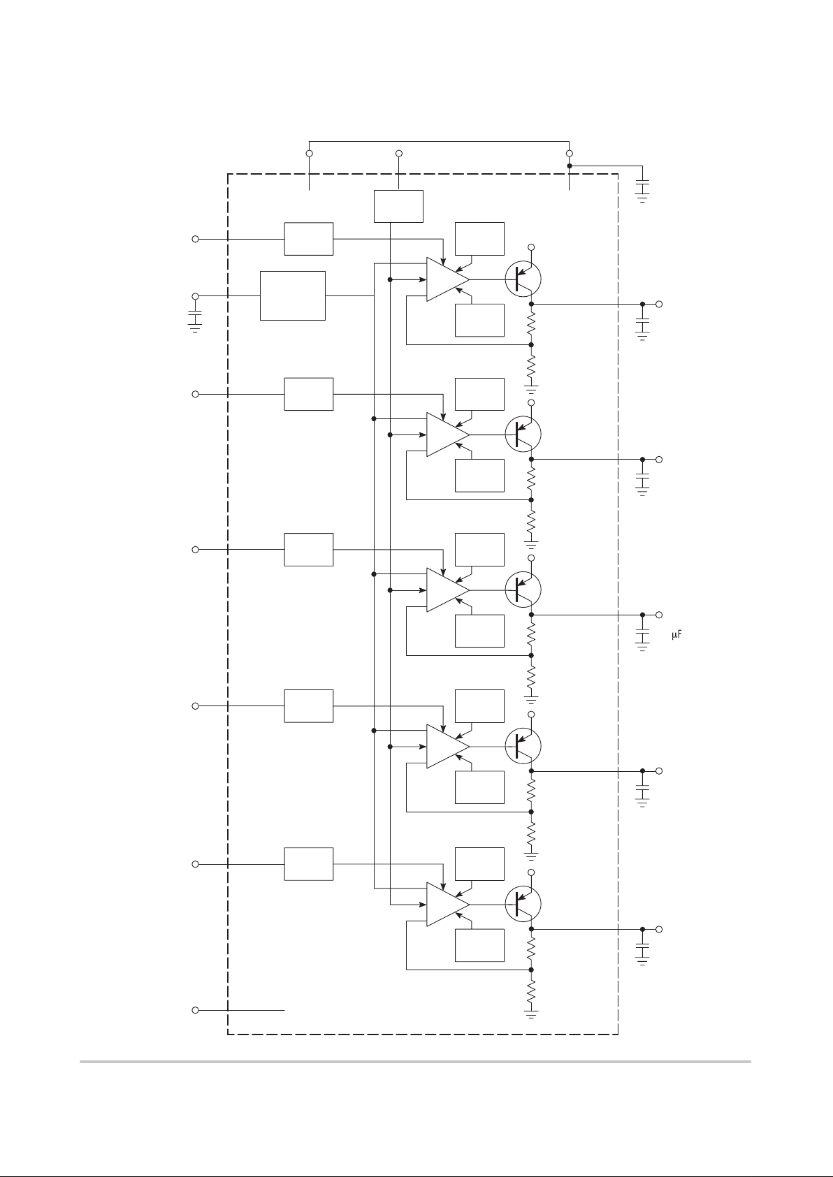
The voltage regulators VR1, VR2 and VR3 have a common input
voltage pin VCC1.
The other voltage regulators VR4 and VR5 have a common input
voltage pin VCC2.
• Five Independent Outputs at 2.8V Typical, based upon voltage
version
• Internal Trimmed Voltage Reference
• V
out
Tolerance ±3.0% over the Temperature Range –40°C to +85°C
• Enable Input Pin (Logic–Controlled Shutdown) for Each of the Five
Outputs
• Common Enable Pin to Shutdown the Whole Circuit
• Very Low Dropout Voltage (0.11 V Typical for Output 1, 2, 3 and 5;
0.17 V Typical for Output 4 at Maximum Current)
• Very Low Quiescent Current (Maximum 5.0 µA in OFF Mode,
130 µA Typical in ON Mode)
• Ultra Low Noise for VR3 (30 µV RMS Max, 100 Hz < f < 100 kHz)
• Internal Current and Thermal Limit
• 100 nF for VR1, VR2, VR4 and VR5 and 1.0 µF for VR3 for
Stability
• Supply Voltage Rejection: 60 dB (Typical) @ f = 1.0 kHz
Device Package Shipping
ORDERING INFORMATION
MC33765DTB TSSOP16 96 Units/Rail
MC33765DTBR2 TSSOP16
TSSOP–16
DTB SUFFIX
CASE 948F
1
16
http://onsemi.com
2500 Units/Reel
MARKING
DIAGRAMS
PIN CONNECTIONS
116
15
14
13
12
11
10
9
2
3
4
5
6
7
8
(Top View)
Bypass
Common Enable
On/Off V–Reg. 1
GND
Not Connected
Output V–Reg. 5
MC33765
On/Off V–Reg. 2
On/Off V–Reg. 3
On/Off V–Reg. 4
On/Off V–Reg. 5 VCC2
Output V–Reg. 4
Output V–Reg. 3
Output V–Reg. 2
Output V–Reg. 1
VCC1
MC33
765
ALYW
1
16
A = Assembly Location
WL, L = Wafer Lot
YY, Y = Year
WW, W= Work Week
MC33765
http://onsemi.com
2
Enable
Current
Limit
Temp.
Shut.
Enable
Current
Limit
Temp.
Shut.
Enable
Current
Limit
Temp.
Shut.
Enable
Current
Limit
Temp.
Shut.
Enable
Current
Limit
Temp.
Shut.
Common
Enable
+
–
+
–
+
–
+
–
+
–
Simplified Block Diagram
330 nF
V
OUT
1
VCC2
(14)
100 nF
V
OUT
2
(13)
100 nF
V
OUT
3
(12)
1.0 mF
V
OUT
4
(11)
100 nF
V
OUT
5
(9)
100 nF
VCC1
VCC1
VCC1
VCC2
VCC2
(8)
GND
(7)
ON/OFF 5
(6)
ON/OFF 4
(5)
ON/OFF 3
VCC1
(4)
ON/OFF 2
BYPASS
(3)
ON/OFF 1
Voltage
Reference
1.25 V
(15) (2)CE
100 nF
(10)
MC33765
http://onsemi.com
3
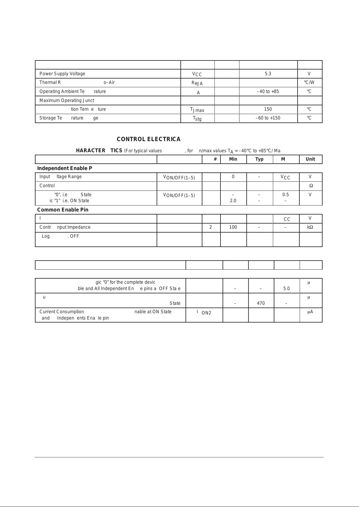
MAXIMUM RATINGS
Rating Symbol Pin # Value Unit
Power Supply Voltage
ÁÁÁÁ
V
CC
5.3
ÁÁÁ
V
Thermal Resistance Junction–to–Air
ÁÁÁÁ
R
q
JA
140
ÁÁÁ
°C/W
Operating Ambient Temperature
ÁÁÁÁ
T
A
–40 to +85
ÁÁÁ
°C
Maximum Operating Junction Temperature
ÁÁÁÁ
T
J
125
ÁÁÁ
°C
Maximum Junction Temperature
ÁÁÁÁ
T
Jmax
150
ÁÁÁ
°C
Storage Temperature Range
ÁÁÁÁ
T
stg
–60 to +150
ÁÁÁ
°C
CONTROL ELECTRICAL CHARACTERISTICS
ELECTRICAL CHARACTERISTICS (For typical values T
A
= 25°C, for min/max values TA = –40°C to +85°C/ Max TJ = 125°C)
Characteristics
Symbol Pin # Min Typ Max Unit
Independent Enable Pins
Input Voltage Range V
ON/OFF(1–5)
0 – V
CC
V
Control Input Impedance
100
–
–
k
W
Logic “0”, i.e. OFF State V
ON/OFF(1–5)
– – 0.5 V
Logic “1”, i.e. ON State 2.0 – –
Common Enable Pin
Input Voltage Range V
CE
2 0 – V
CC
V
Control Input Impedance
2
100
–
–
k
W
Logic “0”, i.e. OFF State V
CE
2 – – 0.3 V
Logic “1”, i.e. ON State 2.0 – –
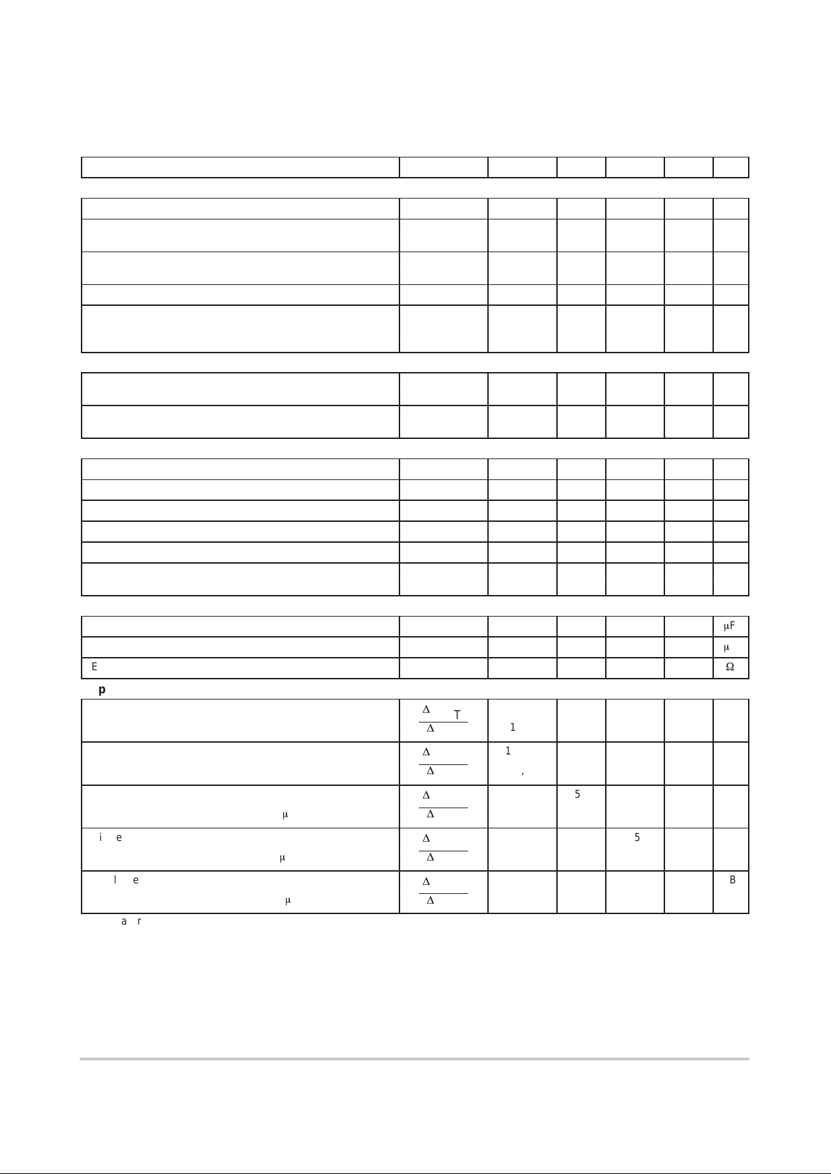
ELECTRICAL CHARACTERISTICS (For typical values T
A
= 25°C, for min/max values TA = –40°C to +85°C/ Max TJ = 125°C)
Characteristics
Symbol Min Typ Max Unit
CURRENT CONSUMPTION with NO LOAD
Current Consumption at Logic “0” for the complete device,
IQ
OFF
m
A
i.e. Common Enable and All Independent Enable pins at OFF State – – 5.0
Current Consumption at Logic “1” for the complete device,
IQ
ON1
m
A
i.e. Common Enable and All Independents Enable pins at ON State – 470 –
Current Consumption at Logic “1”, Common Enable at ON State
IQ
ON2
m
A
and All Independents Enable pins at OFF State – 130 –
MC33765
http://onsemi.com
4
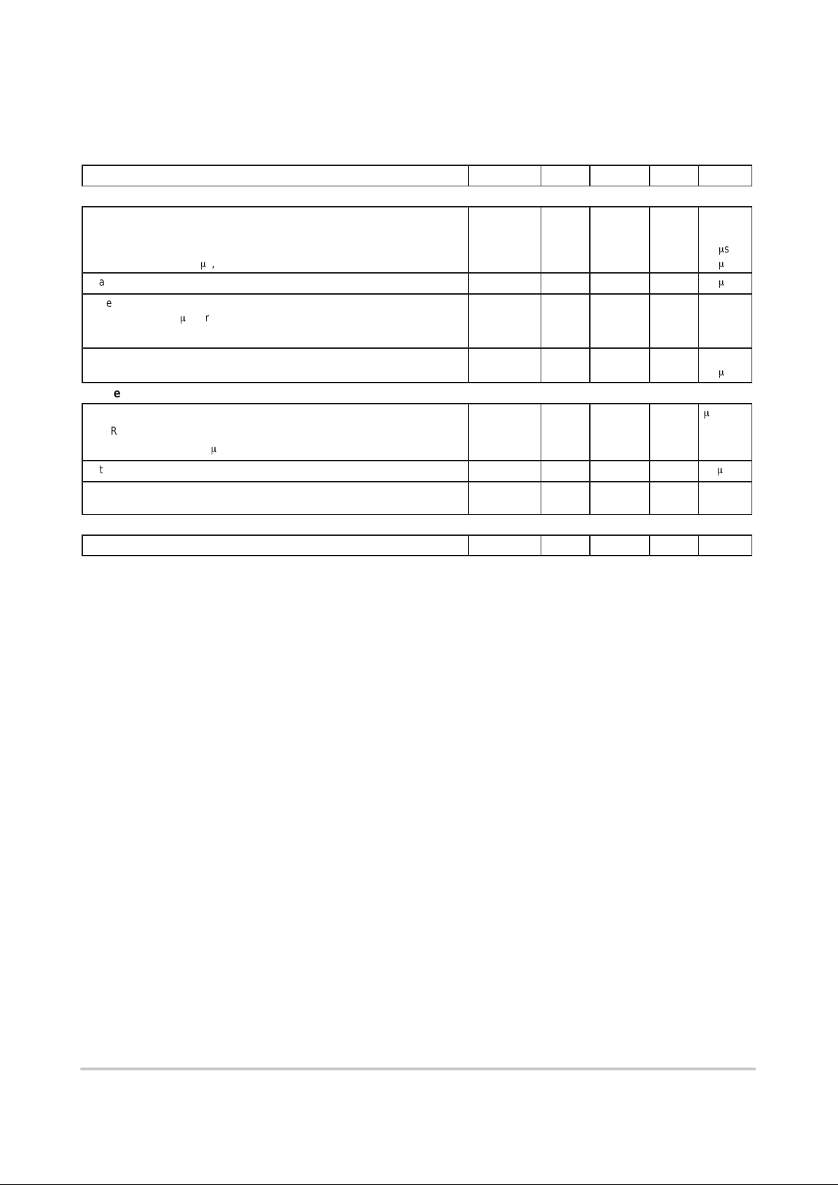
REGULA T OR ELECTRICAL CHARACTERISTICS
ELECTRICAL CHARACTERISTICS (For typical values T
A
= 25°C, for min/max values TA = –40°C to +85°C/ Max TJ = 125°C)
Characteristics Symbol Pin # Min Typ Max Unit
Supply and Output Voltages, Dropout and Load Regulation
Supply Voltage V
CC
MC33765 (2.8V) V
CC1, VCC2
15, 10 3.0 3.6 5.3 V
Regulator Output Voltage for VR1, VR2, VR3, VR4 and VR5 V
OUT(1–5)
14, 13, 12, V
MC33765 (2.8V) 11, 9 2.7 2.8 2.85
Dropout Voltage for VR1, VR2, VR3, VR5 (Note 1.) VCC–V
OUT
14, 13, – 0.11 0.17 V
12, 9
Dropout Voltage for VR4 (Note 1.) VCC–V
OUT4
11 – 0.17 0.30 V
Load Regulation (TA = 25°C) Reg
load(1–5)
9, 11, 12, – – 0.5 mV/
mA
13, 14
Max Power Dissipation and Total DC Output Current (VR1 + VR2 + VR3 + VR4 + VR5) (Note 2.)
Max Power Dissipation at VCC = 5.3 V (TA = 85°C) P
dmax
– – 285 mW
Max. Total RMS Output Current at VCC = 5.3 V (TA = 85°C) I
RMS
– – 130 mA
Max Power Dissipation at VCC = 5.3 V (TA = 25°C) P
dmax
– – 700 mW
Max. Total RMS Output Current at VCC = 5.3 V (TA = 25°C) I
RMS
– – 250 mA
Output Currents (Note 3.)
Regulator VR1 Output Current I
OUT1
14 10 – 30 mA
Regulator VR2 Output Current I
OUT2
13 10 – 40 mA
Regulator VR3 Output Current I
OUT3
12 0 – 50 mA
Regulator VR4 Output Current I
OUT4
11 10 – 150 mA
Regulator VR5 Output Current I
OUT5
9 10 – 60 mA
Current Limit for VR1, VR2, VR3, VR4, VR5 I
MAX
14, 13, 12, – 2 X I
OUT
– mA
[Twice the max Output Current for each output] 11, 9 (1–5)
External Capacitors
External Compensation Capacitors for VR1, VR2, VR4, VR5 C
(1–2, 4–5)
14, 13, 11, 9 0.10 – 1.0
m
F
External Compensation Capacitors for VR3 C
4
12 1.0 – –
m
F
External Compensation Capacitors ESR 0.05 1.0 3.0
W
Ripple Rejections
Ripple Rejection VR1, VR2, VR4, VR5
(DV
OUT
)
14, 13, 50 60 – dB
(at Max. Current, 1.0 kHz, C = 100 nF)
(DVCC)
11, 9
Ripple Rejection VR1, VR2, VR4, VR5
(DV
OUT
)
14, 13, 40 45 – dB
(at Max. Current, f = 10 kHz, C = 100 nF)
(DVCC)
11, 9
Ripple Rejection of VR3
(DV
OUT
)
12 50 60 – dB
(at Max. Current, f = 1.0 kHz, C = 1.0 mF)
(DVCC)
Ripple Rejection of VR3
(DV
OUT
)
12 40 45 – dB
(at Max. Current, f = 10 kHz, C = 1.0 mF)
(DVCC)
Ripple Rejection of VR3
(DV
OUT
)
12 18 22 – dB
(at Max. Current, f = 100 kHz, C = 1.0 mF)
(DVCC)
1. Typical dropout voltages have been measured at currents: Output1: 25 mA, Output2: 35 mA, Output3: 40 mA, Output4: 140 mA, Output5: 40 mA
Maximum value of dropout voltages are measured at maximum specified current.
2. See package power dissipation and thermal protection.
3. Maximum Output Currents are peak values. Total DC current have to be set upon maximum power dissipation specification.
Only Output 3 has been designed to be stable at minimum current of 0 mA.
MC33765
http://onsemi.com
5
REGULA T OR ELECTRICAL CHARACTERISTICS
ELECTRICAL CHARACTERISTICS (For typical values T
A
= 25°C, for min/max values TA = –40°C to +85°C/Max TJ = 125°C)
Characteristics
Symbol Min Typ Max Unit
Dynamic Parameters
Rise Time (1% 99%) Common Enable at ON state,
C
bypass
= 10 nF, I
out
at max. current
VR1, VR2, VR4, VR5 with C
OUT
= 100 nF, TA = 25°C t
on
– – 30
m
s
VR3 with C
OUT
= 1.0 mF, TA = 25°C
– – 150
m
s
Fall Time (99% 1%) [C
OUT
= 100 nF, I
OUT
= 30 mA] (Note 4.) t
off
– 100 –
m
s
Overshoot (C
OUT
= 100 nF for VR1, VR2, VR4, VR5
and C
OUT
= 1.0 mF for VR3) at TA = 25°C
– 5 8 %
Common Enable at ON state, independent enable from OFF to ON state
Settling Time (to ±0.1% of nominal) at TA = 25°C
Common Enable at ON state, independent enable from OFF to ON state – 95 –
m
s
Noise and Crosstalks
Noise Voltage (100 Hz < f < 100 kHz) with C
bypass
= 100 nF
m
V RMS
VR1, VR2, VR4, VR5 with C
OUT
= 100 nF – 40 –
VR3 with C
OUT
= 1.0 mF
– 25 30
Static crosstalk (DC shift) between the Regulator Output, TA = 25°C (Note 5.) – 150 200
m
V
Dynamic CrossT alk Attenuation between the Regulator Outputs 30 35 – dB
(f = 10 kHz), TA = 25°C (Note 6.)
Thermal Shutdown
Thermal Shutdown – 160 – °C
4. The Fall time is highly dependent on the load conditions, i.e. load current for a specified value of C
OUT
.
5. Static Crosstalk is a DC shift caused by switching ON one of the outputs through independent enable to all other outputs. This parameter
is highly dependent on overall PCB layout and requires the implementation of low–noise GROUND rules (e.g. Ground plane).
6. Dynamic crosstalk is the ratio between a forced output signal to signal transferred to other outputs. This requires special device
configuration to be measured.
 Loading...