

Semiconductor Components Industries, LLC, 1999
November, 1999 – Rev. 0
1 Publication Order Number:
MC33761/D
MC33761
Product Preview
Ultra Low-Noise Low
Dropout Voltage Regulator
with 1V ON/OFF Control
The MC33761 is an Low DropOut (LDO) regulator featuring
excellent noise performances. Thanks to its innovative concept, the
circuit reaches an incredible 40µVRMS noise level without an
external bypass capacitor. Housed in a small SOT–23 5 leads–like
package, it represents the ideal designer’s choice when space and
noise are at premium.
The absence of external bandgap capacitor unleashes the response
time to a wake–up signal and makes it stay within 40µs (in repetitive
mode), pushing the MC33761 as a natural candidate in portable
applications.
The MC33761 also hosts a novel architecture which prevents
excessive undershoots when the regulator is the seat of fast transient
bursts, as in any bursting systems.
Finally, with a static line regulation better than –75dB, it naturally
shields the downstream electronics against choppy lines.
Features
• Ultra low–noise: 150nV/√Hz @ 100Hz, 40µVRMS 100Hz – 100kHz
typical, Iout = 60mA, Co=1µF
• Fast response time from OFF to ON: 40µs typical at a 200Hz
repetition rate
• Ready for 1V platforms: ON with a 900mVhigh level
• Nominal output current of 80mA with a 100mA peak capability
• Typical dropout of 90mV @ 30mA, 160mV @ 80mA
• Ripple rejection: 70dB @ 1kHz
• 1.5% output precision @ 25°C
• Thermal shutdown
• Vout available from 2.5V to 5.0V
Applications
• Noise sensitive circuits: VCOs RF stages etc.
• Bursting systems (TDMA phones)
• All battery operated devices
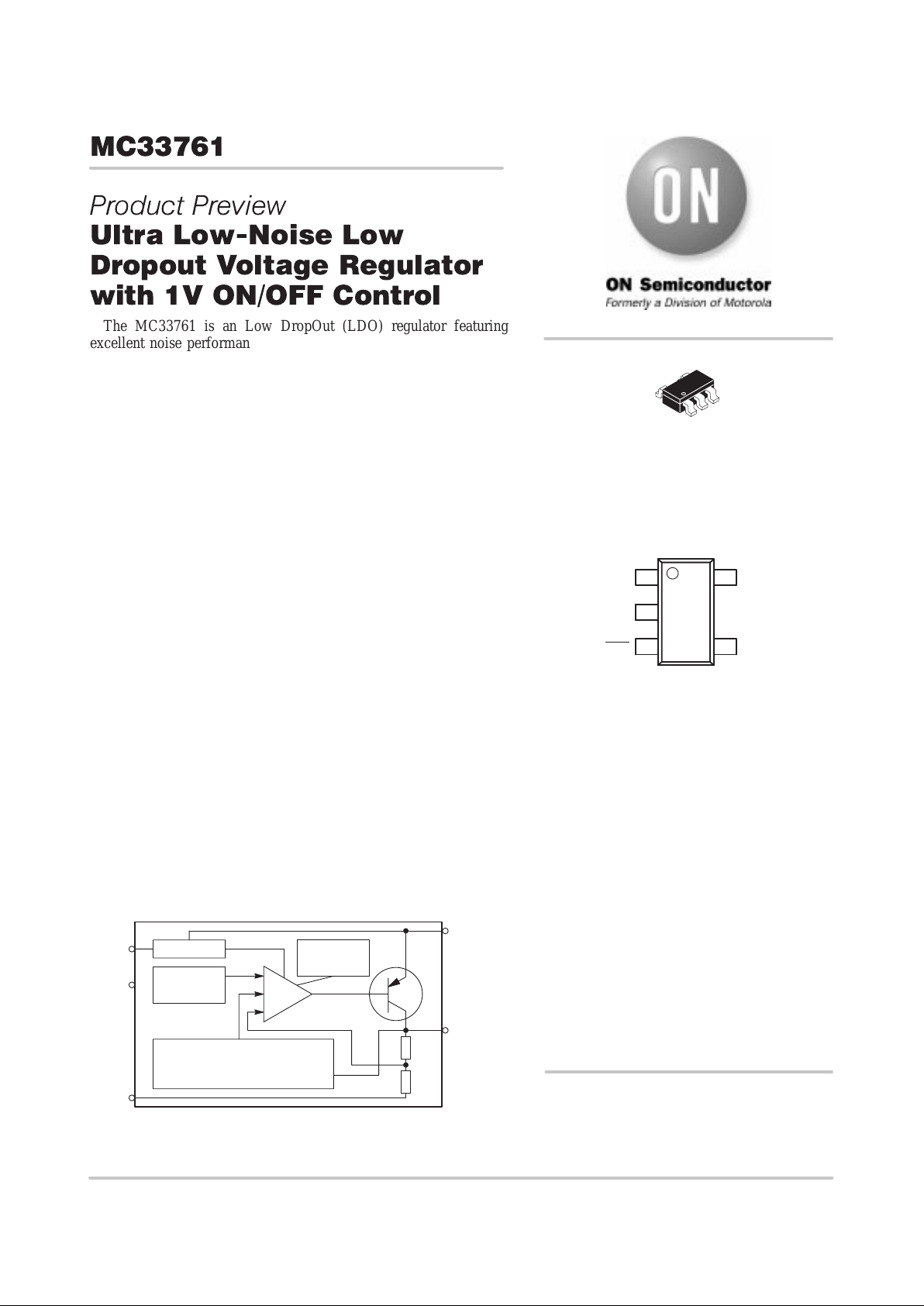
Simplified Block Diagram
Thermal
Shutdown
On/Off
Band Gap
Reference
*Current Limit
*Antisaturation Protection
*Load Transient Improvement
V
out
V
in
GND
NC
ON/
OFF
5
1
2
4
3
This document contains information on a product under development. ON Semiconductor
reserves the right to change or discontinue this product without notice.
TSOP–5
SN SUFFIX
CASE 483
1
http://onsemi.com
5
PIN CONNECTIONS AND
MARKING DIAGRAM
1
3
NC
V
in
2
GND
ON/OFF
4
V
out
5
See detailed ordering and shipping information in the package
dimensions section on page 1 1 of this data sheet.
ORDERING INFORMATION
LxxYW
xx = Version
YW = Date Code
(Top View)
MC33761
http://onsemi.com
2
PIN FUNCTION DESCRIPTIONS
Pin # Pin Name Function Description
1 V
in
Powers the IC A positive voltage up to 12V can be applied upon this pin.
2 GND The IC’s ground
3 ON/OFF Shuts or
wakes–up the IC
A 900mV level on this pin is sufficient to start the IC. A 150mV shuts it down.
4 NC None It makes no arm to connect the pin to a known potential, like in a pin–to–pin
replacement case.
5 V
out
Delivers the
output voltage
This pin requires a 1µF output capacitor to be stable.
MAXIMUM RATINGS
Value
Rating Pin # Symbol Min Max Unit
Power Supply Voltage 1 V
in
— 12 V
ESD Capability, HBM Model All Pins 1 kV
ESD Capability, Machine Model All Pins 200 V
Maximum Power Dissipation
NW Suffix, Plastic Package
Thermal Resistance Junction–to–Air
P
D
R
q
J–A
Internally
Limited
210
W
°C/W
Operating Ambient Temperature
Maximum Junction Temperature
(1)
Maximum Operating Junction Temperature
(2)
T
A
T
Jmax
T
J
–40 to +85
150
125
°C
°C
°C
Storage Temperature Range T
stg
–60 to +150 °C
(1) Internally Limited by Shutdown.
(2) Specifications are guaranteed below this value.
ELECTRICAL CHARACTERISTICS
(For Typical Values TA = 25°C, for Min/Max values TA = –40°C to +85°C, Max TJ = 125°C unless otherwise noted)
Characteristics
Pin # Symbol Min Typ Max Unit
Logic Control Specifications
Input Voltage Range 3 V
ON/OFF
0 V
in
V
ON/OFF Input Resistance (all versions) 3 R
ON/OFF
250
k
W
ON/OFF Control Voltages
(3)
Logic Zero, OFF State, IO = 50 mA
Logic One, ON State, IO = 50 mA
3 V
ON/OFF
900
150
mV
Currents Parameters
Current Consumption in OFF State (all versions)
OFF Mode Current: Vin = V
out
+ 1 V, IO = 0, V
OFF
= 150 mV
IQ
OFF
0.1 2
m
A
Current Consumption in ON State (all versions)
ON Mode Current: Vin = V
out
+ 1 V , IO = 0, VON = 3.5 V
IQ
ON
180
m
A
Current Consumption in ON State (all versions), ON Mode
Saturation Current: Vin = V
out
– 0.5 V , No Output Load
IQ
SAT
800
m
A
Current Limit Vin = Vout
nom
+ 1 V,
Output is brought to Vout
nom
– 0.3 V (all versions)
I
MAX
100 180 mA
(3) Voltage Slope should be Greater than 2 mV/ms
MC33761
http://onsemi.com
3
ELECTRICAL CHARACTERISTICS
(For Typical Values TA = 25°C, for Min/Max values TA = –40°C to +85°C, Max TJ = 125°C unless otherwise noted)
Characteristics
Pin # Symbol Min Typ Max Unit
Output Voltages
V
out
+ 1 V < Vin < 6 V, TA = 25°C, 1 mA < I
out
< 80 mA
2.5 V
5 V
out
2.462 2.5 2.537 V
2.8 V 5 V
out
2.758 2.8 2.842 V
3.0 V 5 V
out
2.955 3.0 3.045 V
3.3 V 5 V
out
3.250 3.3 3.349 V
3.6 V 5 V
out
3.546 3.6 3.654 V
Other Voltages up to 5V Available in 50mV Increments Steps 5 V
out
–1.5 X +1.5 %
V
out
+ 1V < Vin < 6V, TA = –40°C to +85°C, 1m A < I
out
< 80mA
2.5 V
5 V
out
2.425 2.5 2.575 V
2.8 V 5 V
out
2.716 2.8 2.884 V
3.0 V 5 V
out
2.91 3.0 3.090 V
3.3 V 5 V
out
3.201 3.3 3.399 V
3.6 V 5 V
out
3.492 3.6 3.708 V
Other Voltages up to 5V Available in 50mV Increments Steps 5 V
out
–3 X +3 %
Line and Load Regulation, Dropout Voltages
Line Regulation (all versions)
V
out
+ 1 V < Vin < 12 V, I
out
= 80 mA
5/1 Reg
line
20 mV
Load Regulation (all versions)
Vin = V
out
+ 1 V, C
out
= 1 mF, I
out
= 1 to 80 mA
5 Reg
load
40 mV
Dropout Voltage (all versions)
(3)
I
out
= 30 mA
I
out
= 60 mA
I
out
= 80 mA
5
5
5
Vin–V
out
Vin–V
out
Vin–V
out
90
140
160
150
200
250
mV
Dynamic Parameters
Ripple Rejection (all versions)
Vin = V
out
+ 1 V + 1 kHz 100 mVpp Sinusoidal Signal
5/1 Ripple –70 dB
Output Noise Density @ 1 kHz 5 150 nV/
√Hz
RMS Output Noise Voltage (all versions)
C
out
= 1 mF, I
out
= 50 mA, F = 100 Hz to 1 MHz
5 Noise 35
m
V
Output Rise Time (all versions) C
out
= 1 mF, I
out
= 50 mA,
10% of Rising ON Signal to 90% of Nominal V
out
5 t
rise
40
m
s
Thermal Shutdown
Thermal Shutdown (all versions) 125 °C
(3) V
out
is brought to V
out
– 100 mV

MC33761
http://onsemi.com
4
DEFINITIONS
Load Regulation
The change in output voltage for a change in output
current at a constant chip temperature.
Dropout Voltage
The input/output differential at which the regulator output
no longer maintains regulation against further reductions in
input voltage. Measured when the output drops 100mV
below its nominal value (which is measured at 1V
differential value). The dropout level is affected by the chip
temperature, load current and minimum input supply
requirements.
Output Noise Voltage
This is the integrated value of the output noise over a
specified frequency range. Input voltage and output current
are kept constant during the measurement. Results are
expressed in µVRMS.
Maximum Power Dissipation
The maximum total dissipation for which the regulator
will operate within its specs.
Quiescent Current
The quiescent current is the current which flows through
the ground when the LDO operates without a load on its
output: internal IC operation, bias etc. When the LDO
becomes loaded, this term is called the Ground current. It is
actually the difference between the input current (measured
through the LDO input pin) and the output current.
Line Regulation
The change in output voltage for a change in input voltage.
The measurement is made under conditions of low
dissipation or by using pulse technique such that the average
chip temperature is not significantly affected. One usually
distinguishes static line regulation or DC line regulation (a
DC step in the input voltage generates a corresponding step
in the output voltage) from ripple rejection or audio
susceptibility where the input is combined with a frequency
generator to sweep from a few hertz up to a defined
boundary while the output amplitude is monitored.
Thermal Protection
Internal thermal shutdown circuitry is provided to protect
the integrated circuit in the event that the maximum junction
temperature is exceeded. When activated at typically 125°C,
the regulator turns off. This feature is provided to prevent
catastrophic failures from accidental overheating.
Maximum Package Power Dissipation
The maximum power package power dissipation is the
power dissipation level at which the junction temperature
reaches its maximum operating value, i.e. 125°C.
Depending on the ambient temperature, it is possible to
calculate the maximum power dissipation and thus the
maximum available output current.
 Loading...