. . . with single conversion circuitry including oscillator, mixer, IF amplifiers,
limiting IF circuitry, and quadrature discriminator. The MC3374 is perfect for
narrowband audio and data applications up to 75 MHz which require
extremely low power consumption. Battery powered applications down to
VCC = 1.1 V are possible. The MC3374 also includes an on–board voltage
regulator, low battery detection circuitry, a receiver enable allowing a power
down Sleep–Mode, two undedicated buffer amplifiers to allow
simultaneous audio and data reception, and a comparator for enhancing
FSK (Frequency Shift Keyed) data reception to 1200 baud.
• Low Supply Voltage: V
• Low Power Consumption: P
• Input Bandwidth 75 MHz
• Excellent Sensitivity: 0.5 µVrms for 12 dB SINAD
• Voltage Regulator A vailable (Source Capability 3.0 mA)
• Receiver Enable to Allow Active/Standby Operation
• Low Battery Detection Circuitry
• Self Biasing Audio Buffer
• Data Buffer
• FSK Data Shaping Comparator
• Standard 32–Lead QFP Surface Mount Package
Sleep–Mode is a trademark of Motorola, Inc.
= 1.1 to 3.0 Vdc
CC
= 1.5 to 5.0 mW
D
Order this document by MC3374/D
LOW VOLTAGE
SINGLE CONVERSION
FM RECEIVER
SEMICONDUCTOR
TECHNICAL DATA
32
1
FTB SUFFIX
PLASTIC PACKAGE
CASE 873
(Thin QFP)
ORDERING INFORMATION
Tested Operating
Device
MC3374FTB TA = –10° to +70°C TQFP–32
Temperature Range
Package
IF Gnd
V
CC2
1
2
3
4
5
6
7
8
Osc Base
Osc Emit
Isrc Dcpl
Rec Audio
Demodulator Decoupling
Quad T ank
*Internal Connection, do not ground.
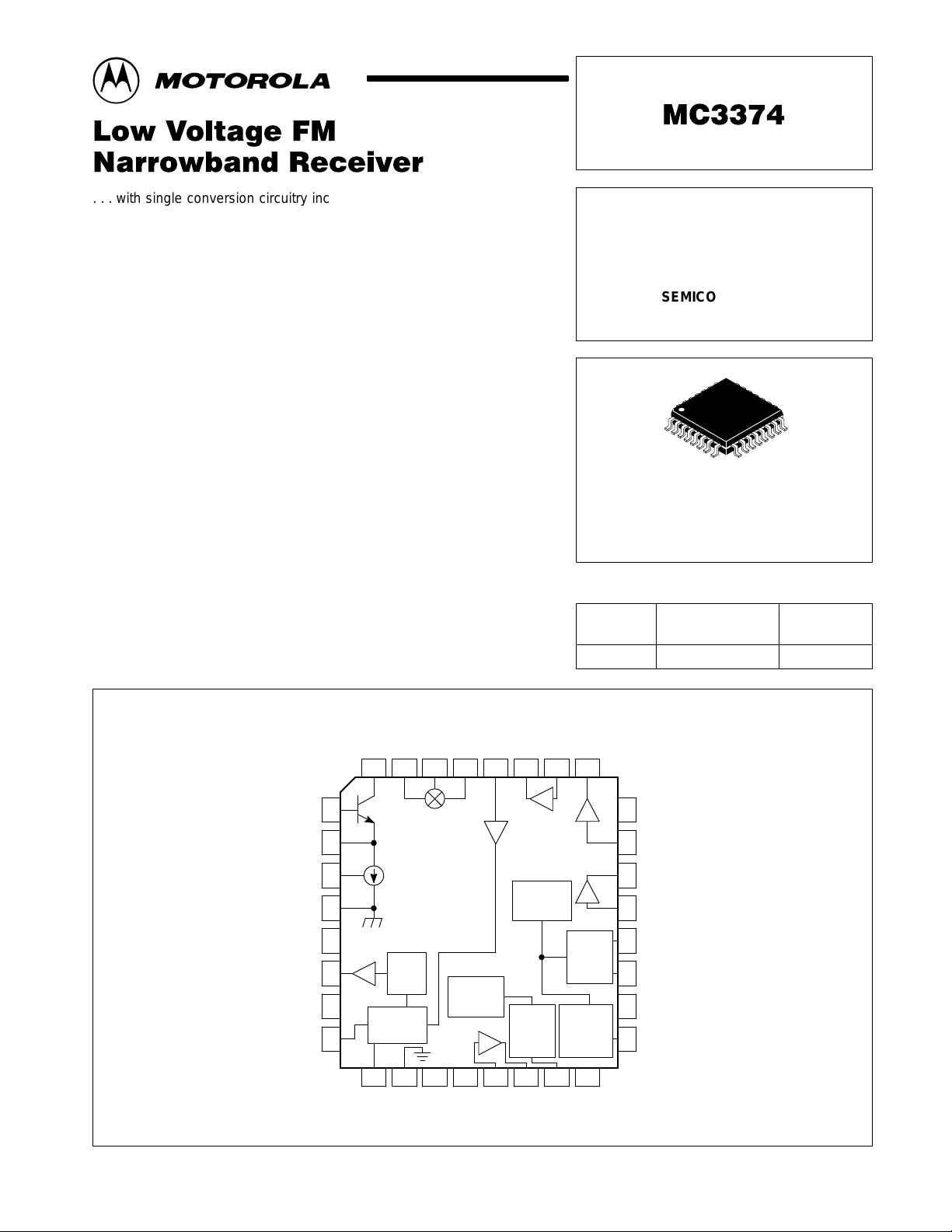
Simplified Block Diagram
Data
Osc
MixerInMixer
Dcpl
32 31 30 29 28 27 26 25
Low
Pass
Output
Buffer
Filter
Quadrature
Demodulator
9 101112131415 16
Quad
Demod
T ank
Gnd
This device contains 87 active transistors
Mixer
Dcpl
2nd IF
Main
Current
Reference
Comp.
2nd IF
In
I/P
Out
Mixer
*N/C *N/C Comp
Buffer
Out
Data
Buffer
Voltage
Reference
Receiver
Enable
Comp
O/P
Enable
Data
Buffer
Rec
1st IF
In
1st IF
Audio
Buffer
Battery
Detector
Voltage
Reference
Regulator
Reference
Out
Low
T est
24
V
CC3
23
1st IF In
22
Audio Buffer Out
21
Audio Buffer In
20
Low Battery Detector
19
1.2 V Select
V
18
CC
17
V
reg
MOTOROLA ANALOG IC DEVICE DATA
Motorola, Inc. 1996 Rev 0
1

MC3374
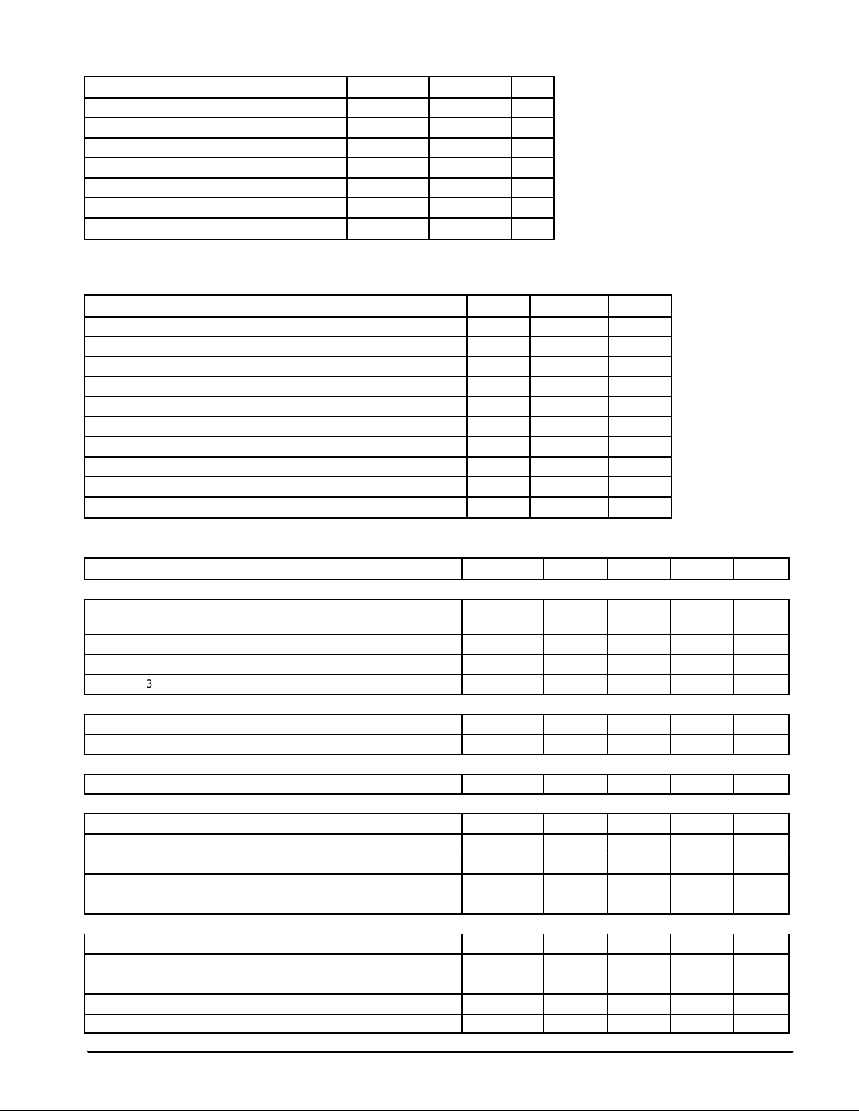
MAXIMUM RATINGS
Supply Voltage 18 5.0 Vdc
RF Input Signal 31 1.0 Vrms
Audio Buffer Input 21 1.0 Vrms
Data Buffer Input 26 1.0 Vrms
Comparator Input 13 1.0 Vrms
Junction Temperature – 150 °C
Storage Temperature – –65 to +150 °C
Device should not be operated at or outside these values. The “Recommended Operating Limits” provide
for actual device operation.
RECOMMENDED OPERATING CONDITIONS
Supply Voltage 18 1.1 to 3.0 Vdc
Receiver Enable Voltage 15 V
1.2 V Select Voltage 19 Open or V
RF Input Signal Level 31 0.001 to 100 mVrms
RF Input Frequency 31 0 to 75 MHz
Intermediate Frequency (IF) – 455 kHz
Audio Buffer Input 21 0 to 75 mVrms
Data Buffer Input 26 0 to 75 mVrms
Comparator Input 13 10 to 300 mVrms
Ambient Temperature – –10 to 70 °C
(Voltage with respect to Pins 4 and 10; TA = 25°C.)
Rating Pin Value Unit
Parameter Pin Value Unit
CC
CC
Vdc
Vdc
ELECTRICAL CHARACTERISTICS (V
Circuit of Figure 1, unless otherwise noted.)
Characteristic
OVERALL MC3374 PERFORMANCE
Drain Current – Pin 15 = VCC (Enabled)
Drain Current – Pin 15 = 0 Vdc (Disabled)
Recovered Audio (RF Input = 10 µV) 6 13 18 30 mVrms
Noise Output (RF Input = 0 mV, 300 Hz–5.0 kHz) 6 – 1.0 – mVrms
Input for –ā3.0 dB Limiting
MIXER
Mixer Input Resistance (Rp) 31 – 1.5 – kΩ
Mixer Input Capacitance (Cp) 31 – 9.0 – pF
FIRST IF AMPLIFIER
First IF Amp Voltage Gain – – 27 – dB
AUDIO BUFFER
Voltage Gain – 3.0 4.0 4.7 V/V
Input Resistance 21 – 110 – kΩ
Maximum Input for Undistorted Output (<5% THD) 21 – 64 – mVrms
Maximum Output Swing (<5% THD) 22 – 690 – mV
Output Resistance 22 – 780 – Ω
DATA BUFFER
Voltage Gain – 1.4 2.7 4.3 V/V
Input Resistance 26 – 9.8 – MΩ
Maximum Input for Undistorted Output (<5% THD) 26 – 100 – mV rms
Maximum Output Swing (<5% THD) 27 – 800 – mV
Output Resistance 27 – 690 – Ω
= 1.3 V, fo = 10.7 MHz, f
CC
= 1.0 kHz, Deviation = 3.0 kHz, TA = 25°C, Test
mod
Pin Min Typ Max Unit
5 + 18 + 24
5 + 18 + 24
31 – 0.6 – µVrms
–
–
1.6
0.5
3.0
–
mA
µA
pp
pp
2
MOTOROLA ANALOG IC DEVICE DATA

MC3374
ELECTRICAL CHARACTERISTICS (continued) (V
= 1.3 V, fo = 10.7 MHz, f
CC
= 1.0 kHz, Deviation = 3.0 kHz, T
mod
A
= 25°C, Test Circuit of Figure 1, unless otherwise noted.)
Characteristic
Pin Min Typ Max Unit
COMPARATOR
Minimum Input for Triggering (RL = 100 kΩ) 13 – 7.0 – mVrms
Maximum Input Frequency (RL = 100 kΩ) 13 – 25 – kHz
Rise Time (10–90%; RL = 100 kΩ) 14 – 5.0 – µs
Fall Time (90–10%; RL = 100 kΩ) 14 – 0.4 – µs
LOW BATTERY DETECTOR
Low Battery Trip Point 19 – 1.2 – Vdc
Low Battery Output – VCC = 0.9 V
Low Battery Output – VCC = 1.3 V
20
20
–
–
0.2
V
CC
–
Vdc
–
VOLTAGE REGULATOR
Regulated Output (see Figure 4) 17 0.95 1.07 1.15 Vdc
Source Capability 17 – – 3.0 mA
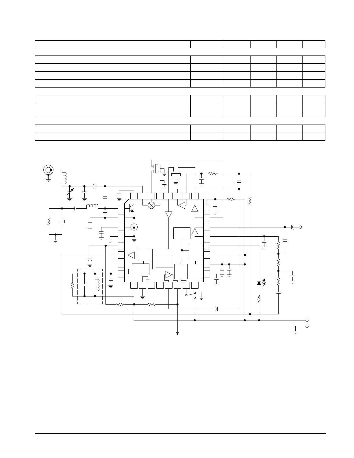
Figure 1. MC3374 Pager IF Application Circuit
RF Input
50
FL1
L1
C
XRD
56 k
C
C1
C2C1
L2
C3
C4
C
10
LC1 100 100 k
C
C2
C3
B
0.1
1
2
3
4
5
Output
6
7
8
C
B
C
32 31 30 29 28 27 26 25
Mixer
MC3374
Buffer
Low
Pass
Filter
Quadrature
Demodulator
9 10111213141516
N.C. N.C.
B
2nd IF
Main
Current
Reference
Comp.
FL2
Data
Buffer
Voltage
Reference
Receiver
Enable
1st IF
Audio
Buffer
Battery
Detector
Voltage
Reference
Enable
Low
0.01
24
23
22
21
20
19
18
17
Disable
180 k
– 330
0.1 10
1.0
4.7
+
0.1
39 k
0.1
µ
F
1.0
8.2 k
8.2 k
3.3 k
0.22
R
L
3900 P
0.022
Audio
Output
NOTES:
1.FL1 and FL2 are 455 kHz ceramic bandpass filters, which should
have input and output impedances of 1.5 kΩ to 2.0 kΩ. Suggested
part numbers are MuRata CFU455X or CFW455x – the ‘X’ suffix
denotes bandwidth.
2.LC1 is a 455 kHz LC resonator. Recommended part numbers are
T oko America RMC2A6597HM or 5SVLC–0637BGT (smaller).
The evaluation board layout shown provides for use of either
resonator. Ceramic discriminator elements cannot be used with
the MC3374 due to their low input impedance. The damping
resistor value can be raised to increase the recovered audio or
lowered to increase the quadrature detector’s bandwidth and
linearity – practical limits are approximately 27 kΩ to 75 kΩ.
Typically the quadrature detector’s bandwidth should match the
low IF filter’s bandwidth.
3.The data buffer is set up as a low–pass filter with a corner
frequency of approximately 200 Hz. The audio buffer is a
bandpass filter with corner frequencies of 300 Hz and 3.0 kHz.
The audio amplifier provides bass suppression.
MOTOROLA ANALOG IC DEVICE DATA
Data Output
V
CC
V
EE
4.CC1 and CC3 are RF coupling capacitors and should have ≤ 20 Ω
impedance at the desired input and oscillator frequencies.
5.CC2 provides “light coupling” of the oscillator signal into the mixer,
and should have a 3.0 kΩ to 5.0 kΩ impedance at the desired
local oscillator frequency.
6.Capacitors labelled CB are bypass capacitors and should have
20 Ω impedance at the desired RF and local oscillator frequencies.
7.The network of L1, C1 and C2 provides impedance matching of
the mixer input (nominally 3.0 kΩ shunted by 9.0 pF) to 50 Ω at the
desired RF/IF input frequency. This will allow for bench testing of
the receiver from typical RF signal generators or radio service
monitors, but additional or different matching will be required to
maximize receiver sensitivity when used in conjunction with an
antenna, RF preamplifier or mixer.
3
 Loading...