Motorola MC33690DW Datasheet
MOTOROLA
SEMICONDUCTOR TECHNICAL
Standalone Tag Reader Circuit
Order this document
by MC33690/D
MC33690
STANDALONE
STARC
The Standalone Tag Reader Circuit (STARC) is an integrated
circuit dedicated to the automotive immobilizer applications. It
combines on the same chip all the circuitry to interface with a
transponder : antenna drivers and demodulator.
A low dropout voltage regulator and a physical interface fully
compatible with the ISO 9141 norm are also available.
The Standalone Tag Reader Circuit is fabricated with the
SMARTMOS
metal, 1.4µm, 45V technology, combining CMOS and bipolar
devices.
• Contactless 125kHz tag reader module :
- Self synchronous sample & hold demodulator
- Amplitude or phase modulation detection
- High sensitivity
- Fast “read after write“ demodulator settling time
- Low resistance and high current antenna drivers :
2Ω @ 150mA (typ.)
- Bidirectionnal data transmission
- Multi tag, multi scheme operation.
• Low dropout voltage regulator :
- Wide input supply voltage range :
from 5.5V up to 40V
- Output current capability up to 150mA DC with an
external power transistor
- 5V output voltage with a ± 5% accuracy
- Low voltage reset function
- Low current consumption in standby mode :
300µA (typ.).
• ISO 9141 transmitter and receiver module :
- Input voltage thresholds ratiometric to the supply
voltage
- Current limitation
- Ouput slew rate control
- No external protection device required.
TM
3.5 technology. This process is a double layer
TAG READER
CIRCUIT
DW SUFFIX
Plastic Package
CASE 751D
SO - 20
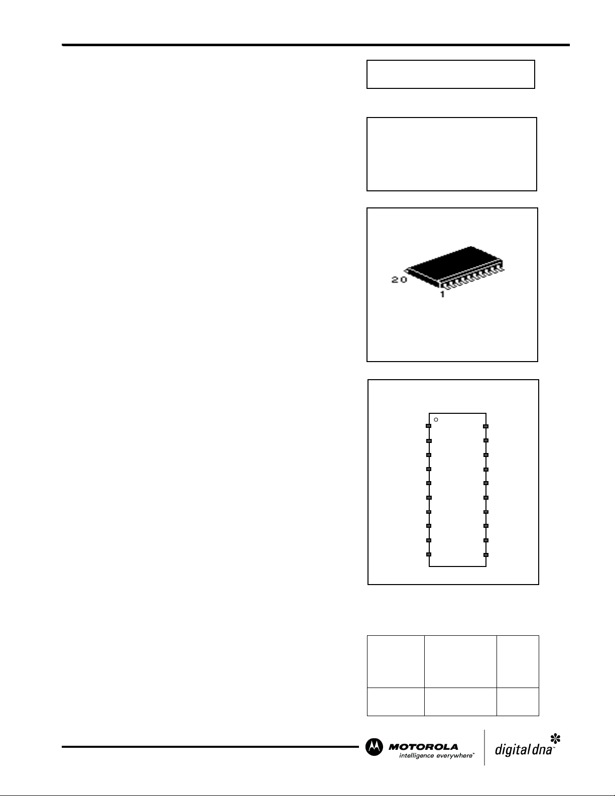
Pin Connections
VSUP
SOURCE
GATE
TD1
VSS
VDD
TD2
MODE1
MODE2
1
2
3
4
5
6
7
8
9
RD
ORDERING INFORMATION
Tx
20
19
Rx
18
K
17
AM
XTAL1
16
XTAL2
15
14
LVR
13
DOUT
12
CEXT
1110
AGND
This document contains information on a new product under development. Motorola
reserves the right to change or discontinue this product without notice.
REV 4.8
© Motorola, Inc., 2002.
Device
MC33690DW
Operating
Junction
Tem p e r a t ure
Range
= -40°C to
T
J
125°C
Package
SOIC 20
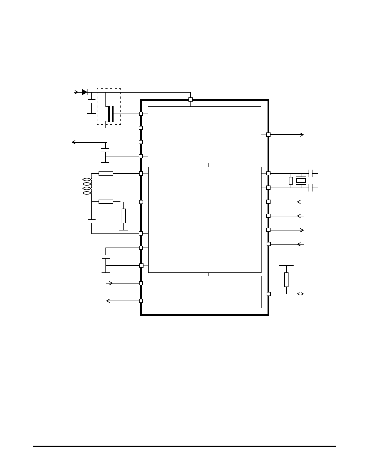
BLOCK DIAGRAM
Optional : external N channel MOS required for sourced current > 50mA.
A recommended reference is MMFT 3055VL from Motorola.
MC33690
Figure 1 : Standalone Tag Reader Circuit
VBAT
VDD
VSUP
C
1
GATE
SOURCE
VDD
10µF
VSS
R
A
L
A
R
1
C
A
C
EXT
10nF
TD1
RD
R
2
TD2
CEXT
AGND
Tx
Voltage Regulator
Tag Reader
LVR
8MHz
XTAL1
XTAL2
MODE1
MODE2
DOUT
AM
VBAT
510Ω
ISO 9141 Interface
Rx
K
© Motorola, Inc., 2002.
MOTOROLA SEMICONDUCTORS PRODUCTS
2
revision 4.8, 5 February 2002
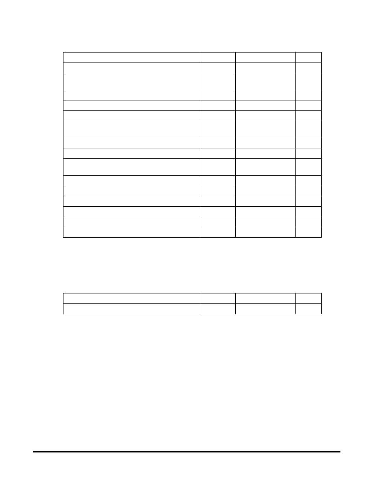
MAXIMUM RATINGS
Supply voltage V
Supply voltage without using the voltage regulator
(V
= VDD)
SUP
Voltage on SOURCE V
Current into/from GATE 0 mA
MC33690
Rating Symbol Value Unit
VSS-0.3 to +40 V
VSS-0.3 to +7 V
-0.3 to +40 V
SS
V
SUP
DD
Voltage on GATE V
Voltage on pins :
MODE1/2, CEXT, DOUT, LVR, XTAL1/2, Rx, Tx
Voltage on RD ±10 V
Voltage on K and AM V
Current on TD1 & TD2
(Drivers on & off)
Voltage on AGND VSS±0.3 V
ESD voltage capability (HBM, see note 1) ±2000 V
ESD voltage capability (MM, see note 1) ±200 V
Solder heat resistance test (10s) 260 °C
Junction temperature T
Storage temperature T
Note 1 :
Human Body model, AEC-Q100-002 Rev. C.
Machine Model, AEC-Q100-003 Rev. E.
THERMAL CHARACTERISTIC
-0.3 V
SS
V
SS
-0.3 to V
-3 to 40 V
SS
+0.3 V
DD
±300 mA
J
s
170 °C
-65 to +150 °C
Junction to ambiant thermal resistance (SOIC20) R
© Motorola, Inc., 2002.
Characteristic Symbol Value Unit
th
MOTOROLA SEMICONDUCTORS PRODUCTS
80 °C/W
revision 4.8, 5 February 2002
3

PIN FUNCTION DESCRIPTION
Pin Function Description
1 VSUP Power supply
2 SOURCE External N channel transistor source
3 GATE External N channel transistor gate
4 TD1 Antenna driver 1 output
5 VSS Power and digital ground
6 VDD Voltage regulator output
7 TD2 Antenna driver 2 output
8 MODE1 Mode selection input 1
9 MODE2 Mode selection input 2
10 RD Demodulator input
11 AGND Demodulator ground
12 CEXT Comparator reference input
MC33690
13 DOUT Demodulator output (5V)
14 LVR Low Voltage Reset input/output
15 XTAL2 Oscillator output
16 XTAL1 Oscillator input
17 AM Amplitude modulation input
18 K ISO 9141 transmitter output and receiver input
19 Rx ISO 9141 receiver monitor output
20 Tx ISO 9141 transmitter input
© Motorola, Inc., 2002.
MOTOROLA SEMICONDUCTORS PRODUCTS
4
revision 4.8, 5 February 2002
DESCRIPTION
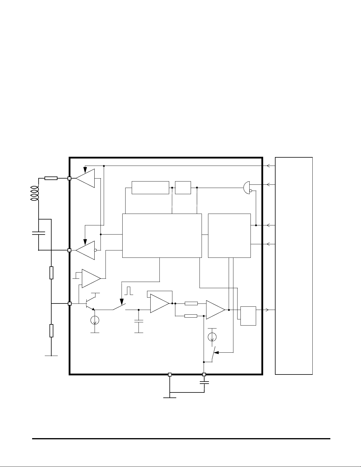
TAG READER MODULE
MC33690
The Tag Reader module is dedicated for
automotive or industrial applications where
information has to be transmitted contactless.
The tag reader module is a write/read (challenge/
response) controller for applications which
demand high security level.
The tag reader module is connected to a serial
tuned LC circuit which generates a magnetic field
power supplying the tag.
Figure 2 : Tag Reader block diagram
R
A
TD1
L
A
125kHz
C
A
1/32 counter 1/2
125kHz
Self synchronous
sample & hold
The use of a synchronous sample & hold
technique allows communication with all
avalaible tags using admittance switching
producing absorption of the RF field.
Load amplitude or phase shift modulation can be
detected at high bit rates up to 8kHz.
125kHz is the typical operational carrier
frequency of the tag reader module with a 8MHz
clock.
AM Data
Clock 8MHz
4MHz
8MHz
Shutdown
Setup & Preload
LVR
TD2
R
1
R
2
-
+
VDD
RD
11.25° , 22.5° , 33.75° , 45° , 56.25° , 67.5° , 78.75° , 90°
+ 0°, -11.25°, -22.5°, -33.75°, -45°, -56.25°, -67.5°, -78.75°
Buffer
500ns
S/H Buffer
+
-
AGND
100K
C
EXT
Comparator
+
Ω
-
VDD
CEXT
10nF
DCQ
500µA
Interface
Data out
© Motorola, Inc., 2002.
MOTOROLA SEMICONDUCTORS PRODUCTS
5
revision 4.8, 5 February 2002
MC33690
Read function
When answering to the base station, a
transponder generates an absorption modulation
of the magnetic field. It results in an amplitude/
phase modulation of the current across the
antenna. This information is picked up at the
antenna tap point between the coil and the
capacitor. An external resistive ladder down
scales this voltage to a level compatible with the
demodulator input voltage range (see parameter
V
page 16).
INRD
The demodulator (see figure 2) consists of :
- an input stage (emitter follower),
- a sample & hold circuit,
- a voltage follower,
- a low offset voltage comparator.
The sampling time is automatically set to take
into account a phase shift due to the tolerances
of the antenna components (L and C) and of the
oscillator. The allowed phase shift measured at
the input RD ranges from -45° to +45°. Assuming
that the phase reference is the falling edge of the
driving signal TD1, this leads to a sampling time
phase ranging from -78.75° to 90° with discrete
steps of 11.25°. After reset condition, the
sampling time phase is +11.25°.
The antenna phase shift evaluation is only
done :
- after each wake-up command (see pages
10 to 12),
- or after reset (see page 7).
This is necessary to obtain the best demodulator
performances.
In order to ensure a fast demodulator settling
time after wake up, reset or a write sequence, the
external capacitor C
is preloaded at its
EXT
working voltage.
This preset occurs 256µs after switching the
antenna drivers on and its duration is 128µs.
After wake up or reset, the preset has the same
duration but begins 518µs after clock settling.
After power on reset, VSUP must meet the
minimum specified value, enabling the nominal
operation of VDD, before the start of the preset.
Otherwise the preset must be done by the user
through a standby/wake-up sequence.
Write function
Whatever the selected configuration (see
page 9), the write function is achieved by
switching on/off the output drivers TD1/2.
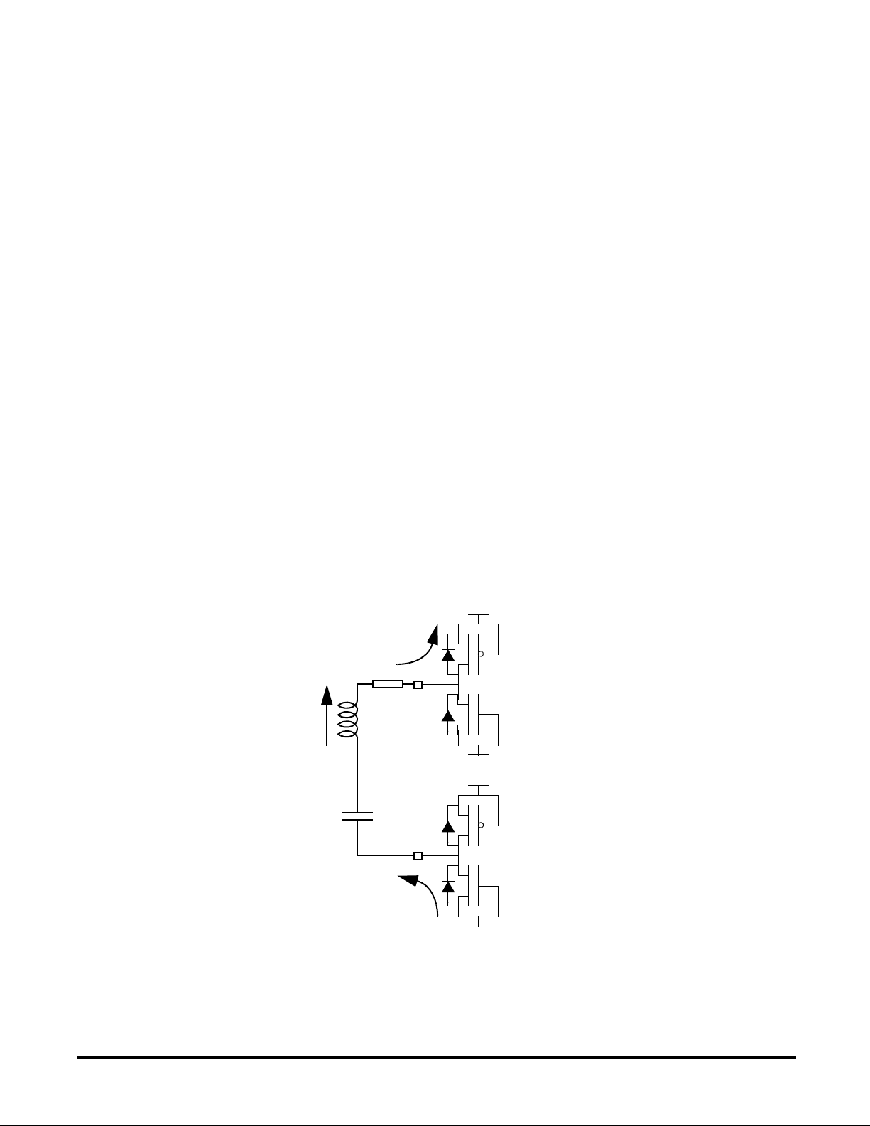
Once the drivers have been set in high
impedance, the load current flows alternatively
Figure 3 : Current flow when the buffers are switched off
VDD
R
A
TD1
I
LOAD
L
A
R
1
C
A
TD2
VDD
© Motorola, Inc., 2002.
MOTOROLA SEMICONDUCTORS PRODUCTS
6
revision 4.8, 5 February 2002
VOLTAGE REGULATOR
MC33690
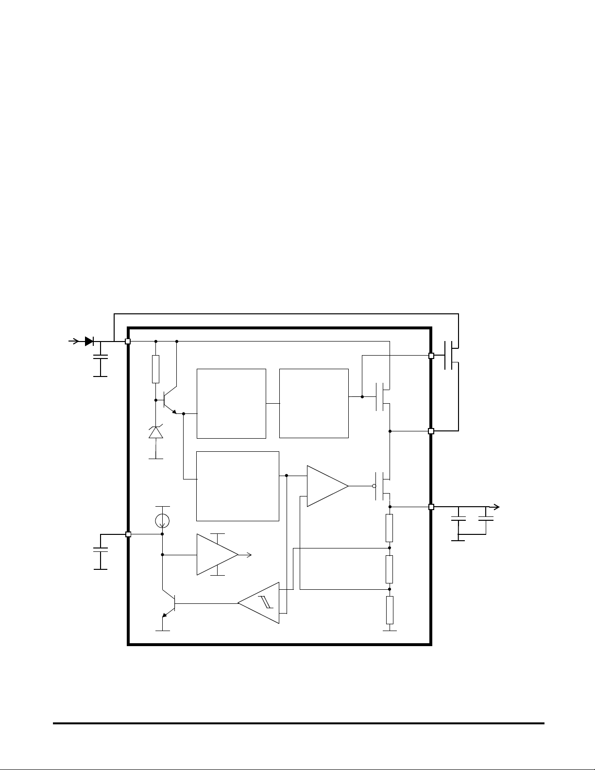
The low dropout voltage regulator provides a
regulated 5V supply for the internal circuitry. It
can also supply external peripherals or sensors.
The input supply voltage ranges from 5.5V to
over 40V.
This voltage regulator uses a series combination
of high voltage LDMOS and low voltage PMOS
transistors to provide regulation. An external low
ESR capacitor is required for the regulator
stability.
The maximum average current is limited by the
power dissipation capability of the SO 20
package.
This limitation can be overcome by connecting
an external N channel MOS in parallel with the
Figure 4 : Voltage regulator block diagram
VBAT
C
1
VSUP
internal LDMOS. The threshold voltage of this
transistor must be lower than the one of the
internal LDMOS (1.95V typ.) in order to prevent
the current from flowing into the LDMOS. Its
breakdown voltage must be higher than the
maximum supply voltage.
A low voltage reset function monitors the VDD
output. An internal 10µA pull-up current source
allows, when an external capacitor is connected
between LVR and GND, to generate delays at
power up (5ms typ. with C
Reset
=22nF) .
The LVR pin is also the input generating the
internal reset signal. Applying a logic low level on
this pin resets the circuit :
- all the internal flip flops are reset,
- the drivers TD1/2 are switched on.
GATE
C
Reset
LVR
VDD
10µA
1MHz oscillator
Voltage reference
and biasing
generator
VDD
reset
Comparator
Charge pump
-
+
N channel
LDMOS
SOURCE
-
+
P channel
MOS
VDD
C
2
10µF
C
3
100nF
VDD
© Motorola, Inc., 2002.
MOTOROLA SEMICONDUCTORS PRODUCTS
7
revision 4.8, 5 February 2002
ISO 9141 PHYSICAL INTERFACE
MC33690
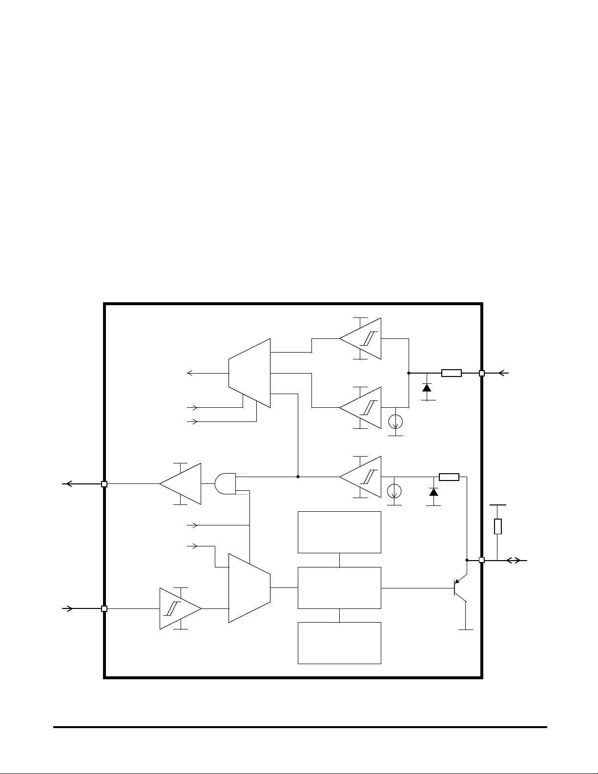
This interface module is fully compatible with
the ISO 9141 norm describing the diagnosis line.
It includes one transmitter (pin K) and 2 receivers
(pins K and AM).
The input stages consist of high voltage CMOS
triggers. The thresholds are ratiometric to VSUP.
A ground referenced current source (2.5µA typ.)
pulls down the input when unconnected.
When a negative voltage is applied on the K or
AM lines, the input current is internally limited by
a 2k
Ω resistor (typ.) in series with a diode.
A current limitation allows the transmitter to drive
Figure 5 : ISO 9141interface
AM data
any capacitive load and protects against short
circuit to the battery voltage. An overtemperature
protection shuts the driver down when the
junction temperature exceeds 150°C (typ). Once
shut down by the overtemperature protection,
the driver can be switched on again :
- if the junction temperature has decreased
below the threshold,
- and by applying an off/on command, coming
either from the demodulator in configurations A
and B or directly applied on the input Tx in
configuration C (see pin K status in table 1 page
9).
The electromagnetic emission is reduced thanks
to the voltage slew rate control (5V/µs typ.).
VDD
2kΩ
VSUP
L line
AM
From configuration controller
VDD
Rx
From configuration controller
Tag Reader module output
VDD
Tx
VSUP
Over temperature
detector
Command
Current limitation
GND
GND
2.5µA
2.5µA
GND
2kΩ
VBAT
GND
K line
K
© Motorola, Inc., 2002.
MOTOROLA SEMICONDUCTORS PRODUCTS
8
revision 4.8, 5 February 2002
 Loading...