

SEMICONDUCTOR
TECHNICAL DATA
HIGH GAIN
LOW POWER
FM IF
Order this document by MC3359/D
P SUFFIX
PLASTIC PACKAGE
CASE 707
DW SUFFIX
PLASTIC PACKAGE
CASE 751D
(SO–20L)
Crystal
Osc.
NC
CASE 707
CASE 751D
50 k
9
–
+
52 k
Limiter
Demodulator
1.8 k
Demod
Output
Recovered
Audio
Filter
Input
Filter
Output
Demodulator
Filter
Decoupling
20
Quadrature
Input
19
18
17
16
15
14
13
12
1110
9
8
7Decoupling
Limiter
Input
V
CC
Mixer
Output
6
1
2
3
4
Crystal
Osc.
Demodulator
Filter
Quadrature
Input
Decoupling
Decoupling
Limiter
Input
V
CC
Mixer
Output
Recovered
Audio
Demod
Output
10
16
15
514
13
12
Audio
Mute
18
NC
10 pF
RF
Input
Scan
Control
Squelch
Input
Filter
Output
Filter
Input
RF
Input
6
7
8
2
3
4
Gnd
1
17
Gnd
Squelch
Input
Audio
Mute
11
5
Scan
Control
Broadcast Detector
Mixer
Oscillator
1.8 k
MC3359DW
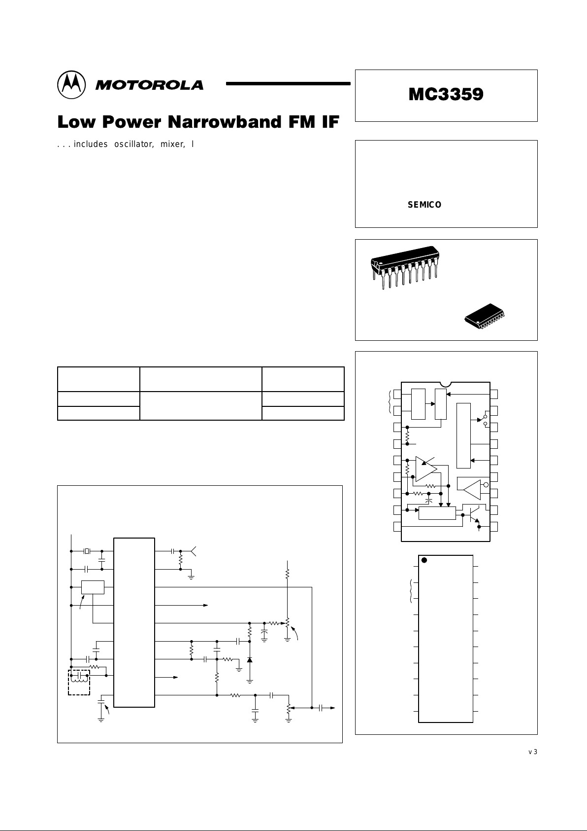
Figure 2. Pin Connections and
Functional Block Diagram
1
MOTOROLA ANALOG IC DEVICE DATA
...includes oscillator, mixer, limiting amplifier, AFC, quadrature
discriminator, op/amp, squelch, scan control, and mute switch. The MC3359
is designed to detect narrowband FM signals using a 455 kHz ceramic filter
for use in FM dual conversion communications equipment. The MC3359 is
similar to the MC3357 except that the MC3359 has an additional limiting IF
stage, an AFC output, and an opposite polarity Broadcast Detector. The
MC3359 also requires fewer external parts. For low cost applications
requiring VCC below 6.0 V, the MC3361BP,BD are recommended. For
applications requiring a fixed, tuned, ceramic quadrature resonator, use the
MC3357. For applications requiring dual conversion and RSSI, refer to these
devices; MC3335, MC3362 and MC3363.
• Low Drain Current: 3.6 mA (Typical) @ V
CC
= 6.0 Vdc
• Excellent Sensitivity: Input Limiting Voltage –
– 3.0 dB = 2.0 µV (Typical)
• Low Number of External Parts Required
• For Low Voltage and RSSI, use the MC3371
ORDERING INFORMATION
Device
Operating
Temperature Range
Package
MC3359DW
–
°
SO–20L
MC3359P
T
A
= –30 to +
70°C
Plastic DIP
0.01 µF
Input
VCC = 6.0 Vdc
Audio
Out
Audio
Volume
0.002
µ
F
7.5 k
0.01
µ
F
10 k
Recovered Audio
Automatic
Frequency
Control
390 k
0.001
µ
F
18 k
1N4148
750
0.001
µ
F
0.1
µ
F
120 k
50 k
Squelch
Sensitivity
.47
µ
F
+
68 k
Inverting
Op Amp
(Filter)
Ceramic
Filter
220 pF
V
CC
= 6.0 Vdc
68 pF
MC3359
0.1 µF
0.1 µF
68 k
Quad
Coil
100 pF
0.1
µ
F
51
Mute
Scan Control
Squelch Input
Output
Type
CFU
455 D
51 k
Toko
Type
7MC–8128Z
10.7 MHz
Input
10.245 MHz
910
8
11
712
613
514
415
316
1
18
172
Figure 1. Simplified Application in a Scanner Receiver
Figure 2.
Motorola, Inc. 1996 Rev 3
MC3359
2
MOTOROLA ANALOG IC DEVICE DATA
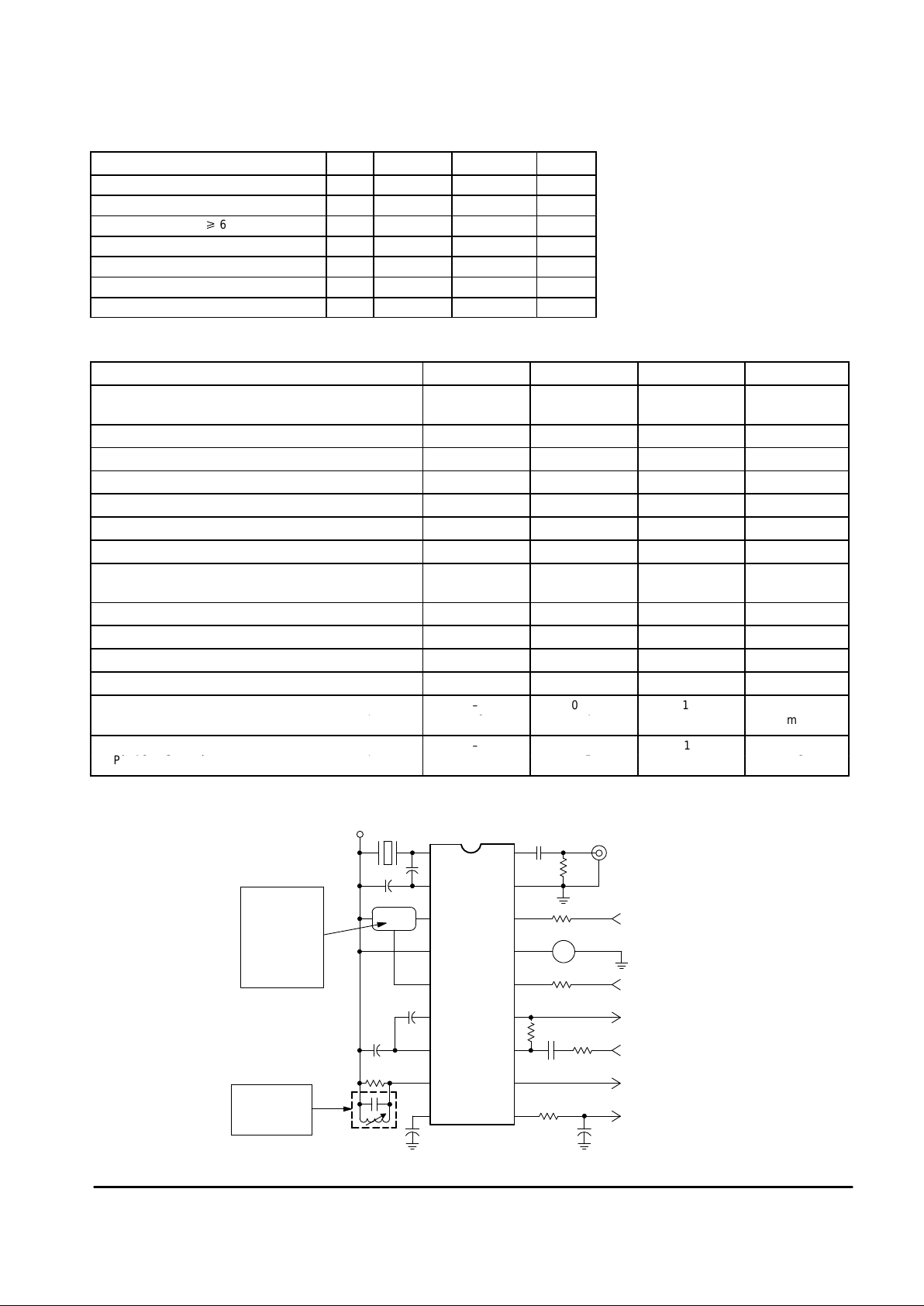
MAXIMUM RATINGS
(TA = 25°C, unless otherwise noted)
Rating
Pin Symbol Value Unit
Power Supply Voltage 4 VCC(max) 12 Vdc
Operating Supply Voltage Range 4 V
CC
6 to 9 Vdc
Input Voltage (VCCq
6.0 Volts) 18 V
18
1.0 V
rms
Mute Function 16 V
16
– 0.7 to 12 V
pk
Junction Temperature – T
J
150 °C
Operating Ambient Temperature Range – T
A
– 30 to + 70 °C
Storage Temperature Range – T
stg
– 65 to + 150 °C
ELECTRICAL CHARACTERISTICS (V
CC
= 6.0 Vdc, fo = 10.7 MHz, ∆f = ± 3.0 kHz, f
mod
= 1.0 kHz, 50 Ω source, TA = 25°C test circuit
of Figure 3, unless otherwise noted)
Characteristics
Min Typ Max Units
Drain Current (Pins 4 and 8) Squelch Off
Squelch On
–
–
3.6
5.4
6.0
7.0
mA
Input for 20 dB Quieting – 8.0 – µVrms
Input for – 3.0 dB Limiting – 2.0 – µVrms
Mixer Voltage Gain (Pin 18 to Pin 3, Open) – 46 –
Mixer Third Order Intercept, 50 Ω Input – – 1.0 – dBm
Mixer Input Resistance – 3.6 – kΩ
Mixer Input Capacitance – 2.2 – pF
Recovered Audio, Pin 10
(Input Signal 1.0 mVrms)
450 700 – mVrms
Detector Center Frequency Slope, Pin 10 – 0.3 – V/kHz
AFC Center Slope, Pin 11, Unloaded – 12 – V/kHz
Filter Gain (test circuit of Figure 3) 40 51 – dB
Squelch Threshold, Through 10K to Pin 14 – 0.62 – Vdc
Scan Control Current, Pin 15 Pin 14 – High
–
0.01
1.0 µA
g
Pin 14 – Low 2.0 2.4 –
µ
mA
Mute Switch Impedance
Pin 14 – High
– 5.0
10 Ω
p
Pin 16 to Ground
g
Pin 14 – Low 1.5 – MΩ
0.1 µF
Op Amp Output
Audio Gen.
0.7 Vp–p
Squelch Input
10 k
AFC Output
Op Amp Input
10.245 MHz
V
CC
68
pF
220 pF
Audio Output
1
17
2.4 k
2
muRata
CFU455D
or
Kyocera
KBF455P–20A
3
7.5 k
4
I
+
1.0 M
1.0 k
1.0
µ
F
0.002
µ
F
15
14
13
12
11
18
Ceramic
Filter
10
16
9
Lp = 1.0 mH
Cp = 120 pF
Rp = 100 k
Ω
8
0.1
µ
F
7
100 pF
6
68 k
5
0.1
µ
F
Input
10.7 MHz
51
Figure 3. Test Circuit
MC3359
3
MOTOROLA ANALOG IC DEVICE DATA
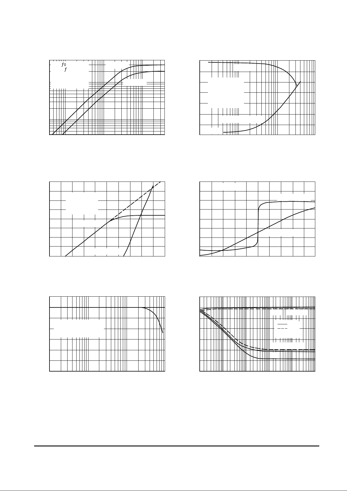
– 2.0– 4.0– 6.0– 8.0 4.0 6.0 8.0
4.0
6.0
10
20
40
60
100
200
400
100101.00.1
– 70
– 60
– 50
– 40
– 10
– 30
– 20
0
FREQUENCY [MHz]
10
Figure 4. Mixer Voltage Gain
INPUT, 50 Ω (mVrms)
75
°
C
25
°
C
VCC = 6.0 Vdc
10010
5.0
–90 –80
– 20
– 10
10
10
0
0.1
20
0
10
–70 –60 –50 –40
– 40
4.0
0.1 1.0
– 20
–30
– 30
– 40
– 50
– 60
0.001
INPUT [mVrms]
1.00.01
400.1 1.00.04
– 30
10
–20 –10
3.0
010
–10
–20
–40
–50
2.0
1.0
0
– 10
RELATIVE FREQUENCY [kHz]
FREQUENCY [MHz]
100
2.00
0
–60
10
– 60
8.0
– 50
7.0
6.0
INPUT, 50
Ω
[dBm]
– 10
RELATIVE GAIN [dB]
RELATIVE OUTPUT [dB] OUTPUT [Vdc]
RELATIVE OUTPUT [dB]
OUTPUT, 1.8 K [dBm]
–30
INPUT LEVEL, 50 [dBm]
Ω
Ω
OUTPUT, 1.8 K [mVrms]
Ω
Input po = 10.7 MHz
Output
p
0 = 455 kHz
Output taken at
Pin 3 with filter
removed (open)
VCC = 9.0 V
VCC = 6.0 V
Figure 5. Limiting IF Frequency Response
100 µV
Response Taken on
a special prototype.
Terminals not
available on
standard device.
IF Output
IF Input for –3 dB LImiting
Figure 6. Mixer Third Order
Intermodulation Performance
Output taken at
Pin 3 with filter
removed
VCC = 6.0 Vdc
Desired Products
3rd Order IM Products
Figure 7. Detector and AFC Responses
VCC = 6.0 Vdc
AFC Output Pin 11
Detector Output Pin 10
Derived using optimum L/C
oscillator values and holding
IF frequency at 455 kHz
Figure 8. Relative Mixer Gain Figure 9. Overall Gain, Noise, and AM Rejection
S+N±3 KHz FM
S + N (30% AM)
N
 Loading...