

SEMICONDUCTOR
TECHNICAL DATA
200 mA INTELLIGENT LDO
REGULATOR WITH SMART
BYPASS CONTROL
Order this document by MC33565/D
D SUFFIX
PLASTIC PACKAGE
CASE 751–06
(SO–8)
Pins 2 and 5 Not Connected
8
1
+5 V
in
N/C
+3.3 V
in
Gnd
Drive out
+3.3 V
out
Sense in
N/C
1
2
3
4
8
7
6
5
MC33565
Device Type Package
ORDERING INFORMATION
MC33565D
3.3V
SO–8
1
MOTOROLA ANALOG IC DEVICE DATA
The MC33565 Low Dropout Regulator is designed for computer
peripheral card applications complying with the
instantly available
requirements
as specified by ACPI objectives. The MC33565 permits
glitch–free transitions from “sleep” to “active” system modes and has internal
logic circuitry to detect whether the system is being powered from the
motherboard main 5V power supply or the 3.3V aux supply.
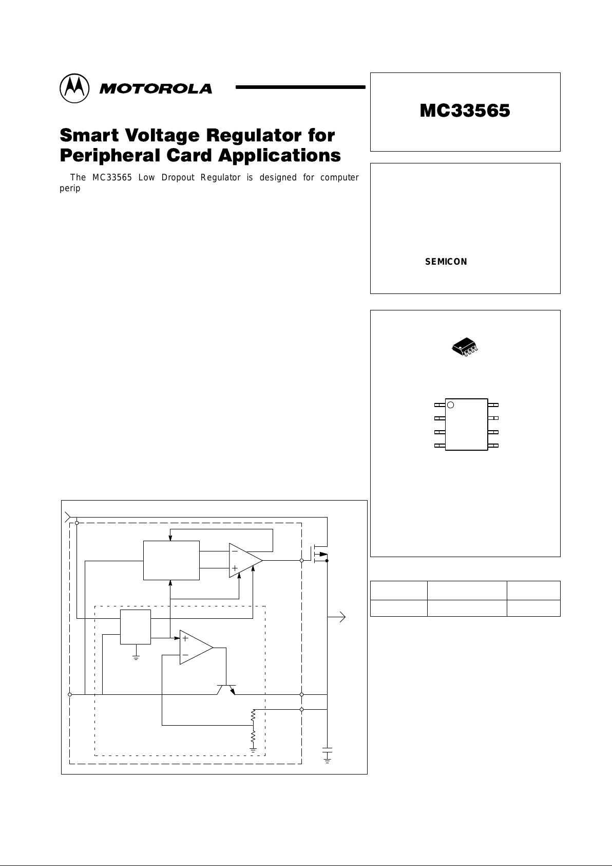
The MC33565 provides a regulated output voltage of 3.3V via either an
internal low drop out 5.0V–to–3.3V voltage regulator or an external P–channel
MOSFET , depending on the operating status of the system in which the card is
installed. During normal operating mode (5V main supply available) the 3.3V
output is provided from the internal low dropout regulator at an output current
of 200mA. When the motherboard enters sleep mode, the MC33565 operates
from the 3.3V aux supply and routes the aux current to the output via the
external P–channel MOSFET bypass transistor controlled by the
drive out
pin.
As a result, the output voltage provided to the peripheral card remains
constant at 3.3V even during transitions to and from sleep mode.
MC33565 Features:
• Output Regulated to 2% Over Temperature
• Output current up to 200mA
• Excellent Line and Load Regulation
• Low Dropout V oltage
• Prevents reverse current flow during sleep mode
• Glitch–free transfer from sleep mode to active mode
• Compatible with
Instantly Available
PC systems
• Evaluation Kit Available: (P.N. MC33565EVK)
Simplified Block Diagram
V
ref
Compensation
&
Hysteresis
+5 Vin
Ref &
Detect
5V detect
Comp
Driver
Drive out
+3.3 Vout
Sense in
+3.3 Vin
Hyst sw
External
P–channel
MOSFET
+3.3 Vout
External
4.7
µ
F
cap
LDO
Motorola, Inc. 1999 Rev 0, 6/99
MC33565
2
MOTOROLA ANALOG IC DEVICE DATA
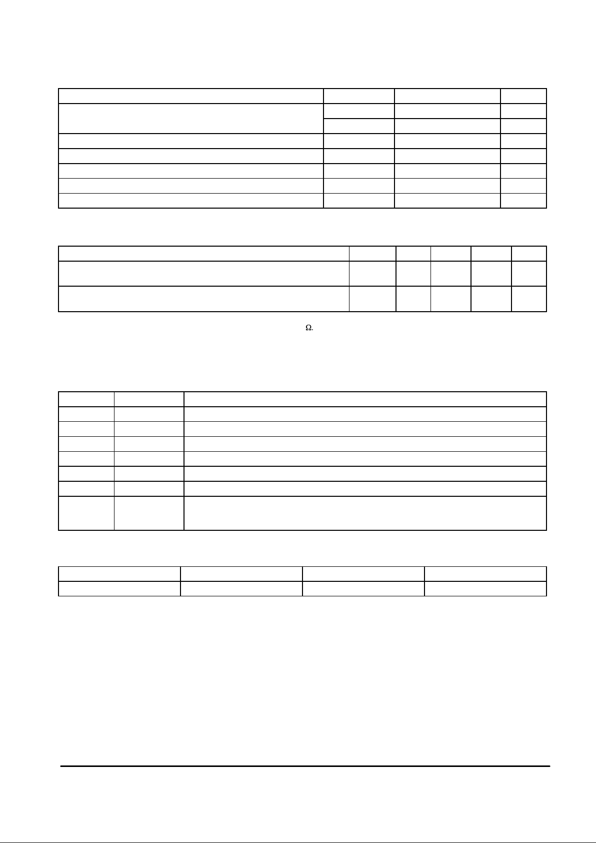
MAXIMUM RATINGS
(TC = 25°C, unless otherwise noted)
Parameter Symbol Max Value Unit
Input Voltage, V
CC
V
max
7.0 Vdc
V
min
–0.5 Vdc
Operating Ambient Temperature T
a
–5 to +70 °C
Operating Junction Temperature T
J
– 5 to +150 °C
Lead Temperature (Soldering, 10 seconds) T
L
300 °C
Storage Temperature Range T
stg
– 55 to +150 °C
Package Thermal Resistance, Junction to Ambient R
θJA
1
180 °C/W
NOTES: 1. Mounted on recommended minimum PCB pad on FR4, 2–oz. copper circuit board.
AC ELECTRICAL SPECIFICATIONS
(3) (4)
Parameter Symbol Min Typ Max Unit
Drive High Delay (Vin ramping up)
C
Drive
= 1.2 nF, measured from +5 Vin = V
thresHi
to V
Drive
= 2V
t
DH
0.5 3.5 µS
Drive Low Delay (Vin ramping down)
C
Drive
= 1.2 nF, measured from +5 Vin = V
thresLo
to V
Drive
= 2V
t
DL
0.5 3.5 µS
NOTES: (1.) See 5V Detect Thresholds Diagram.
(2.) Recommended source impedance for 5V supply: ≤ 0.25W. This will ensure that Io x R
source
< V
hyst
, thus avoiding
driveout toggling during 5V detect threshold transitions.
(3.) See Figure 2. Application Block Diagram.
(4.) See Timing Diagram.
PIN ASSIGNMENTS AND FUNCTIONS
PIN # PIN NAME PIN DESCRIPTION
1 +5 V
in
This is the input supply for the IC. Typical voltage 5 V.
(1) (2)
2,5 N/C Reserved
3 +3.3 V
in
Auxiliary input. Typical voltage 3.3 V.
4 Gnd Logic and Power Gnd.
6 Sense in Load–sense voltage input to internal regulator.
7 +3.3 V
out
3.3V output provided to the application circuit (output current is sourced to this pin from the 5V input.)
8 Drive out
This output drives a P–channel MOSFET with up to 2000pF of “effective” gate capacitance.
Recommended device is MGSF1P02EL T MOSFET. Drive out has active internal pull–up and
pull–down circuitry to guarantee fast transitions.
DEVICE MARKING
Device Type Sub–type Marking (1st Line)
MC33565D 3.3 V MC565
MC33565
3
MOTOROLA ANALOG IC DEVICE DATA
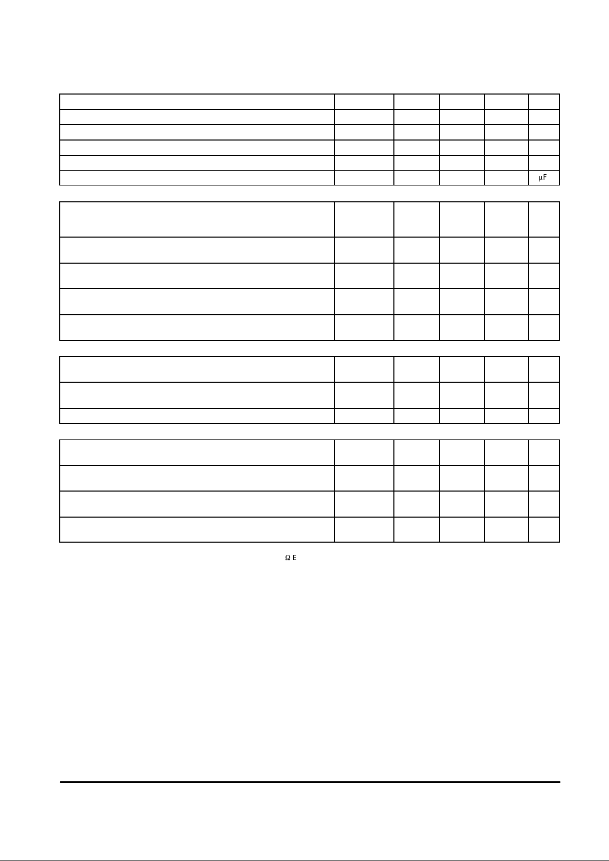
DC ELECTRICAL CHARACTERISTICS
(1)
Characteristic Symbol Min Typ Max Unit
+5 Vin Supply Voltage Range +5 V
in
4.3 5.0 5.5 Vdc
Reverse Leakage Current from Output I
reverse
— — 25 µA
V
Aux
quiescent current — — 3.0 mA
+5 Vin quiescent current, operating — — 10 mA
Load Capacitance
(2)
C
load
4.7 22 —
m
F
REGULATOR OUTPUT
Output Voltage
(4.3V ≤ Vin ≤ 5.5V , 0mA ≤ Io ≤ 200mA) TA = 25°C
(TA = –5°C to 150°C)
+3.3 V
out
3.267
3.234
3.30
3.30
3.333
3.366
Vdc
In–to–Out Voltage
(3.9V ≤ Vin ≤ 4.3V , V
aux
= 3.3V)
V
d
3.0 — — Vdc
Voltage Out at Max Voltage In
(Vin = 7V)
V
outmax
3.1 3.3 3.5 Vdc
Line Regulation
(Io = 200 mA)
— — 0.4 %
Load Regulation
(Io = 0 to 200 mA)
— — 0.4 %
5V DETECT
Low Threshold Voltage
(+5 Vin falling)
V
thresLo
3.9 4.05 4.3 Vdc
High Threshold Voltage
(+5 Vin rising)
V
thresHi
— 4.2 4.3 Vdc
Hysteresis V
Hyst
0.12 0.15 0.18 Vdc
DRIVE OUTPUT
Output peak source Current
(+5 Vin > V
thresHi
)
I
peak
15 — — mA
Output peak sink Current
(+5 Vin < V
thresLo
)
I
peak
15 — — mA
Low Output Voltage
(IoL = 200 µA, Vin < V
thresLo
)
V
oL
— 100 200 mVdc
High Output Voltage
(IoH = 200 µA)
V
oH
3.4 V5–0.8 — Vdc
NOTE: 1. (–5°C<Ta<70°C, 4.3V<5V<5.5V , C
load
= 4.7µF unless otherwise noted)
NOTE: 2. 4.7µF minimum over temperature; 22µF recommended; 500mW ESR maximum.
 Loading...