

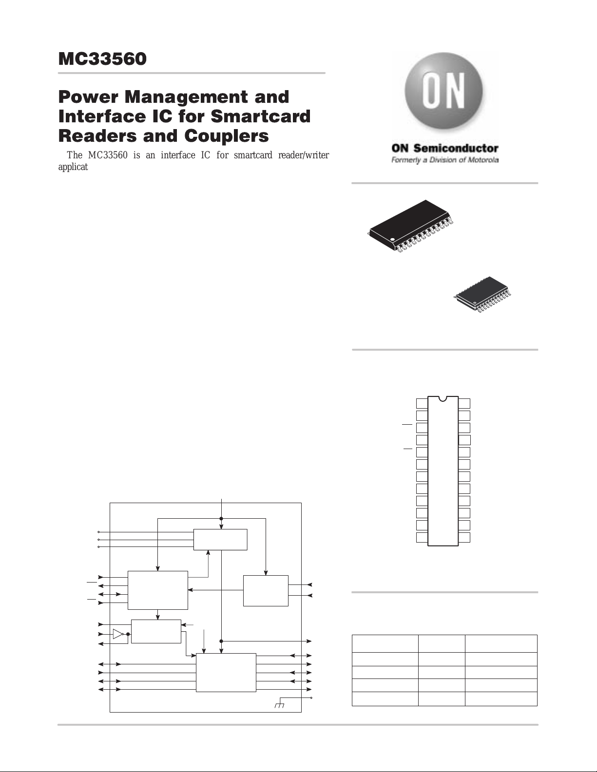
MC33560
Power Management and
Interface IC for Smartcard
Readers and Couplers
The MC33560 is an interface IC for smartcard reader/writer
applications. It enables the management of any type of smart or memory
card through a simple and flexible microcontroller interface. Moreover,
several couplers can be coupled in parallel, thanks to the chip select input
pin (pin #5). The MC33560 is particularly suited to low power and
portable applications because of its power saving features and the
minimum of external parts required. Battery life is extended by the wide
operating range and the low quiescent current in stand by mode. A highly
sophisticated protection system guarantees timely and controlled
shutdown upon error conditions.
• 100% Compatible with ISO 7816–3 Standard
• Wide Battery Supply Voltage Range: 1.8V < V
• Programmable V
Supply for 3V or 5V Card Operation
CC
• Power Management for Very Low Quiescent Current in Stand By
Mode (30µA max)
• Microprocessor Wake–up Signal Generated Upon Card Insertion
• Self Contained DC/DC Converter to Generate V
of Passive Components
• Controlled Power Up/Down Sequence for High Signal Integrity on
the Card I/O and Signal Lines
• Programmable Card Clock Generator
• Chip Select Capability for Parallel Coupler Operation
• High ESD Protection on Card Pins (4kV, Human Body Model)
• Fault Monitoring V
BATlow
, V
CClow
and I
CClim
• All Card Outputs Current Limited and Short Circuit Protected
• T ested Operating Temperature Range: –25°C to +85°C
Figure 1. Simplified Functional Block Diagram
VBAT
ILIM
PGND
PWRON
INT
RDYMOD
CS
L1
POWER
MANAGER
AND
PROGRAMMING
DC/DC
CONVERTER
< 6.6V
BAT
using a Minimum
CC
CARD
DETECTOR
DELAY
CRDDET
CRDCON
24
DTB SUFFIX
http://onsemi.com
1
TSSOP–24
CASE 948H
24
PIN CONNECTIONS
124
PGND
PWRON
RDYMOD
INVOUT
ASYCLKIN
SYNCLK
CRDGND
2
INT
3
4
CS
5
RESET
6
7
IO CRDCON
8
9
10
11
CRDIO CRDRST
12
(Top View)
23
22
21
20
19
18
17
16
15
14
13
SO–24L
DW SUFFIX
CASE 751E
1
ILIM
VBAT
L1
C4
C8
CRDC8
CRDDET
CRDC4
CRDCLK
CRDVCC
SYNCLK
ASYCLKIN
INVOUT
IO
RESET
C4
C8
Semiconductor Components Industries, LLC, 1999
October, 1999 – Rev. 0
CLOCK
GENERATOR
VBAT
LEVEL
TRANSLATOR
ORDERING INFORMATION
CRDVCC
CRDIO
CRDRST
CRDC4
CRDC8
CRDCLK
CRDGND
1 Publication Order Number:
Device Package Shipping
MC33560DW
MC33560DWR2
MC33560DTB
MC33560DTBR2
SO–24WB 30 Units/Rail
SO–24WB 1000 Tape & Reel
TSSOP–24 62 Units/Rail
TSSOP–24 2500 Tape & Reel
MC33560/D
MC33560
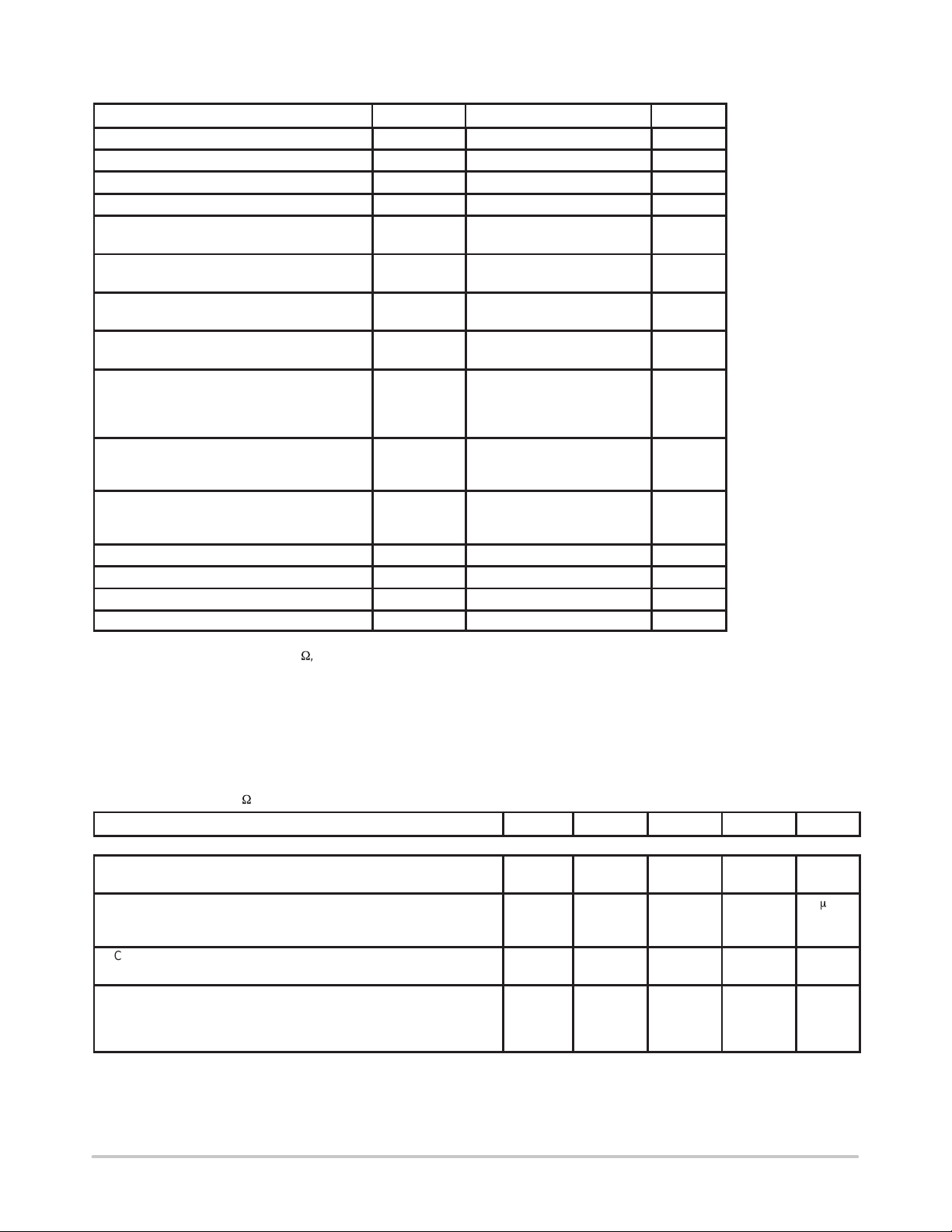
MAXIMUM RATINGS (Note 1)
Rating
Battery Supply Voltage V
Battery Supply Current I
Power Supply Voltage V
Power Supply Current I
Digital Input Pins
(2, 4, 5, 6, 7, 9, 10, 17, 18, 20, 21)
Digital Output Pins (3, 4, 8) V
Card Interface Pins (11, 13, 14, 15, 16, 19) V
Coil Driver Pin (22), ILIM (pin 24)
Power Ground (pin 1)
ESD Capability: (Note 2)
Standard Pins (2, 3, 4, 5, 6, 7, 8, 9, 10, 17, 18,
20, 21, 22, 23, 24)
Card Interface Pins (11, 13, 14, 15, 16, 19)
SO–24WB Package:
Power Dissipation @ TA = 85 °C
Thermal Resistance Junction to Air
TSSOP–24 Package:
Power Dissipation @ TA = 85 °C
Thermal Resistance Junction to Air
Operating Ambient Temperature Range T
Operating Junction Temperature Range T
Max. Junction Temperature (Note 3) T
Storage Temperature Range T
Note 1: Maximum electrical ratings are those values beyond which damage to the device may. TA = 25°C
Note 2: Human body model, R = 1500W, C = 100pF
Note 3: Maximum thermal rating beyond which damage to the device may occur
This device contains protection circuitry to guard against damage due to high static voltages or electric fields. However precautions must be
taken to avoid applications of any voltage higher than maximum rated voltages to this high impedance circuit. For proper operation, input
and output voltages should be constrained to the ranges indicated in the recommended operating conditions.
Symbol Value Unit
BAT
BAT
CC
V
I
OUT
I
OUT
Card
I
Card
V
ESD
P
R
θJAs
P
R
θJAt
Jmax
CC
IN
IN
I
L
Ds
Dt
A
stg
– 0.5 to VBAT + 0.5 but < 7
– 0.5 to VBAT + 0.5 but < 7
– 0.5 to VCC + 0.5
J
7 V
± 200 mA
6 V
± 150 mA
± 5
±10
± 25
± 200
± 100
2
4
285
140
220
180
– 40 to + 85 °C
– 40 to + 125 °C
150 °C
– 65 to + 150 °C
V
mA
V
mA
V
mA
mA
kV
kV
mW
°C/W
mW
°C/W
ELECTRICAL CHARACTERISTICS These specifications are written in the same style as common for standard
integrated circuits. The convention considers current flowing into the pin (sink current) as positive and current flowing out of the pin
(source current) as negative. (Conditions: V
85°C, L1 =47µH, R
BATTERY POWER SUPPLY SECTION
Supply Voltage Range
normal operating range extended operating range (Note 4)
MC33560 Stand By Quiescent Current
PWRON = GND, CRDCON = GND, ASYCLKIN = GND, V
all other logic inputs and outputs open
DC Operating Current
–ICC = 10mA ; VCC =5V ,V
V
undervoltage detection:
BAT
Upper Threshold
Lower Threshold
Hysteresis
Note 4: See figures 2 and 3.
=0W, CRDVCC capacitor=10µF, unless otherwise noted.)
LIM
Characteristic
= 6V
BAT
= 4V, VCC = 5V nom, PWRON = V
BAT
= 6V,
BAT
, operating mode, –ICC = 10mA, –25°C ≤ TA ≤
BAT
Symbol Min Typ Max Unit
V
BAT
I
oBAT
I
BATop
2.2
1.8
6.0
6.6
30
12.5 mA
1.6
1.4
0.2
http://onsemi.com
2
V
m
s
V
MC33560
VCC = 5V NOMINAL POWER SUPPLY SECTION
Characteristic
Output Voltage 2.2V v V
Card VCC Undervoltage Detection:
Upper Threshold
Lower Threshold
Switching Hysteresis
Peak Output Current VCC = 4V, internally limited
Current limit time–out VCC = 4V t
Start–up Current VCC = 2V; 0°C to +85°C
Low Side Switch Saturation Voltage IL = 50mA, pin 22 V
Rectifier on Saturation Voltage IL = 50mA, pin 22 to pin 13 V
Converter Switching Frequency TA = 25 °C f
Shut Down Current
(Card access deactivated)
VCC = 3V NOMINAL POWER SUPPLY SECTION (V
Characteristic
Output Voltage 2.2V v V
Card VCC Undervoltage Detection:
Upper Threshold
Lower Threshold
Switching Hysteresis
Start–up Current
Shut Down Current
(Card access deactivated)
APPLICATION INTERFACE DC SECTION (V
Characteristic
Input High Threshold Voltage
(increasing)
Input Low Threshold Voltage
(decreasing)
Switching Hysteresis pins 2, 4, 5, 6, 10, 17 V
Threshold Voltage pin 9
Pull–down resistance VIN = V
Pull–up resistance VIN = 0.5V, pin 3, 4, 5 R
Output High Voltage IOH = –2.5µA, pin 3, pin 4 for CS = H
Output Low Voltage IOL = 1.0 mA, pins 7, 20, 21
Input Leakage Current VIN = 2.5V, CS = H, pins 9, 17, 18,
1mA v –ICC v 10mA
2.5V v V
1mA v –ICC v 50mA
(RDYMOD output)
(see table 4)
VCC = 2V
PWRON = GND, VCC = 2V
pins 2, 4, 5, 6, 10, 17 V
pins 2, 5, 6, 10
pin 17
pin 4
pin18
IOH = –50µA, pins 7, 20,21
IOH = –0.2mA, pin 8
pin 4 ( in output mode)
IOL = 0.2mA, pins 3, 4, 8
20, 21
Test Conditions Symbol
v 6V
1mA v –ICC v 25mA
3.0V v V
1mA v –ICC v 60mA
(RDYMOD output)
(see table 4)
(RDYMOD = L)
PWRON = GND, VCC = 2V I
BAT
v 6V
BAT
–40°C to 0°C
= 2.5V, –ICC = 5mA)
BAT
Test Conditions Symbol
v 6V
BAT
v 6V
BAT
= 5V)
BAT
Test Conditions Symbol
–1V, pin 2, 6, 7, 10 R
BAT
Guaranteed Limits
Min Typ Max
V
CC
V
T5H
V
T5L
V
HYS5
–I
CClim
d
–I
CCst
sat22
Fsat22
sw
SD
V
CC
V
T3H
V
T3L
V
HYS3
–I
CCst
I
SD
IH
V
IL
HYST
V
TH
down
up
V
OH
V
OL
+/–Ileak 2.0
4.75
4.60
4.2
120
80 mA
80
50
80 mA
Min Typ Max
2.75
2.60
2.4
80
50
50
Min Typ Max
0.55*V
BAT
0.3*V
BAT
0.2*V
BAT
0.3*V
BAT
0.06*V
BAT
0.5*V
BAT
0.4*V
BAT
120 240 500
120 240 500
V
–1 V
BAT
5.0
5.0
VCC–0.14 V
4.5
180
160 ms
100 160 mV
400 520 mV
120 kHz
Guaranteed Limits
3.0
3.0
VCC–0.1
2.7
110
Guaranteed Limits
0.65*V
0.45*V
0.40*V
0.5*V
0.3*V
0.6*V
0.6*V
5.25
5.40
3.25
3.40
0.4 V
BAT
BAT
BAT
BAT
BAT
BAT
BAT
Unit
V
mV
mA
Unit
V
V
V
mV
mA
Unit
V
V
V
V
k
W
k
W
m
A
http://onsemi.com
3
MC33560
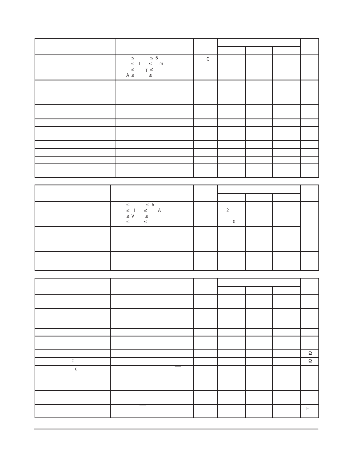
CARD INTERFACE DC SECTION (V
Characteristic
Output High Voltage IOH = –20µA, pin 11, 16, 19
Output Low Voltage IOL = 1mA, pins 11, 16, 19
I/O Pull–up resistance, operating
mode, CS
Card pins security voltage
(Card access deactivated)
Note 5: the transistors T1 on lines IO, C4 and C8 (see figure 24) have a max Rdson of 250W.
DIGITAL DYNAMIC SECTION (V
Input Clock Frequency pin 9, duty cycle = 50% f
Card Clock Frequency pin 15 f
Card Clock Duty Cycle (Note 7) pin 15, 50% to 50% VCC ,
Card Clock Rise and Fall Time pin15, 10% ↔ 90% V
I/O Data Transfer Frequency pin [7, 11], [21, 16], [20, 19] (Note 8) f
I/O Duty Cycle pin [7, 11], [21, 16], [20, 19] (Note 8)
I/O Rise and Fall Time pin [7, 11], [21, 16], [20, 19] (Note 8)
I/O Transfer Time pin [7, 11], [21, 16], [20, 19] (Note 8)
Card Signal Sequence Interval pin 11, 14, 15, 16, 19,
Card Detection Filter Time:
Card insertion
Card extraction
Internal Reset Delay RES, VCC power up/down t
Ready Delay Time pin 4 t
PWRON low Pulse Width CS = L, pin 2 t
Note 6: Pin loading=30pF, except INVOUT=15pF
Note 7: As the clock buffer is optimized for low power consumption and hence not symmetrical, clock signal duty cycle is guaranteed for
divide by 2 and divide by 4 ratio.
Note 8: In either direction
DIGITAL DYNAMIC SECTION (V
Data Setup Time
RDYMOD, PWRON, RESET, IO
Data Hold Time
RDYMOD, PWRON, RESET, IO
CS low Pulse Width pin 5 t
=L, PWRON =H
Characteristic Test Conditions Symbol Min Typ Max Unit
Characteristic Test Conditions Symbol Min Typ Max Unit
= 5V)
BAT
Test Conditions Symbol
Min Typ Max
V
IOL = 0.2mA, pins 14, 15
IOL = 0.2mA, pins 14, 15
VOL = 0.5V , pin 11, 16, 19 18
PWRON = GND, lin=10mA, pin 11,
14, 15, 16, 19
= 5V, normal operating mode, Note 6)
BAT
fio = 16MHz
CC
50% to 50% V
10% ↔ 90% V
50% to 50% VCC , L H, H L
VCC power up/down
= 5V, programming mode, Note 6)
BAT
pin 2, 4, 6, 7 t
pin 2, 4, 6, 7 t
CC
CC
OH
V
OL
V
security
asyclk
crdclk
r
clk
t
rclk
r
t
rio
t
t
dseq
t
fltin
t
fltout
dres
drdy
won
smod
hmod
wcs
VCC –0.9 V
45 55 %
, t
fclk
io
io
, t
fio
tr
45 55 %
50
50
2.0
1.0
1.0
2.0
Guaranteed Limits
Guaranteed Limits
1.0 MHz
0.2 1.0
20
Guaranteed Limits
Unit
0.4 V
2.0 V
20 MHz
20 MHz
10 ns
150 ns
100 ns
150
150
2.0
k
W
m
s
m
s
m
s
m
s
m
s
m
s
m
s
m
s
m
s
http://onsemi.com
4
MC33560
IBATop
(
A)
I
(
A)
IBATop
M
(
A)
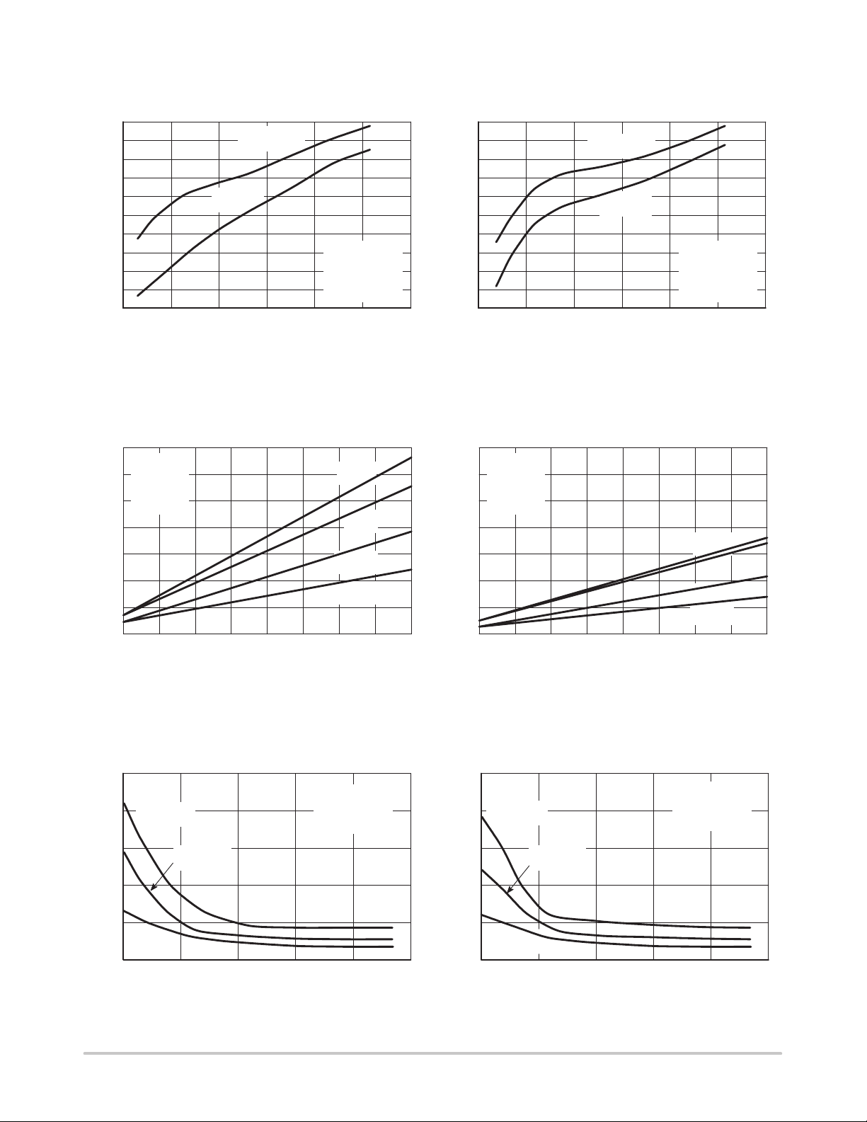
Figure 2. Maximum Battery and Card Supply
Current vs. V
200
180
160
140
120
m
100
80
60
40
20
0
1.5
2.5 3.5 7.5
ICC MAX
(V
CC
=5V)
BAT
IBATop MAX
4.5 5.5 6.5
VBAT (V)
Mode Sync
SYNCLK=4MHz
L1=47µH
Rlim=0
Figure 4. Battery Current vs. Input Clock Frequency
(ICC=0, V
14
VBAT=4V
12
L1=47µH
Rlim=0
10
ICC=0
m
8
6
4
2
0
2.0 4.0 6.0 8.0 10
0
Frequency (MHz)
BAT
=4V)
Async
Sync
Async/2
Async/4
12 14 16
Figure 3. Maximum Battery and Card Supply
200
180
160
140
120
100
I (mA)
Current vs. V
IBATop MAX
80
60
40
20
0
1.5
2.5 3.5 7.5
(VCC=3V)
BAT
ICC MAX
4.5 5.5 6.5
VBAT (V)
Mode Sync
SYNCLK=4MHz
L1=47µH
Rlim=0
Figure 5. Battery Current vs. Input Clock Frequency
(I
14
12
10
8
6
IBATop (mA)
4
2
0
=0, V
CC
VBAT=2.5V
L1=47µH
Rlim=0
ICC=0
2.0 4.0 6.0 8.0 10
0
Frequency (MHz)
BAT
=2.5V)
Async
Sync
Async/2
Async/4
12 14 16
Figure 6. Maximum Battery Current vs. R
(VCC=5V, V
250
200
L1=100µH
m
150
ax
100
50
L1=22µH
0
0
L1=47µH
12
Rlim (ohms)
=4V)
BAT
Mode Sync
SYNCLK=4MHz
VBAT=4V
34
LIM
5
Figure 7. Maximum Battery Current vs. R
250
200
150
100
IBATop Max (mA)
50
L1=22µH
0
0
(VCC=3V, V
L1=100µH
L1=47µH
12
Rlim (ohms)
BAT
=2.5V)
LIM
Mode Sync
SYNCLK=4MHz
VBAT=2.5V
34
5
http://onsemi.com
5
MC33560
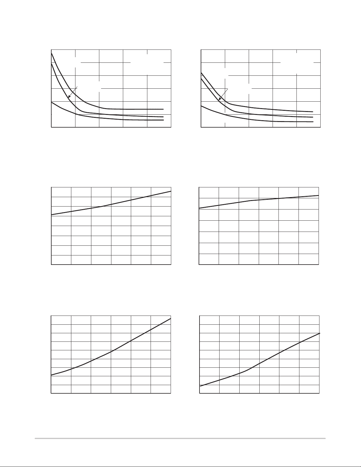
Figure 8. Maximum Card Supply Current
vs. R
120 120
L1=100µH
100
80
60
ICC Max (mA)
40
20
L1=22µH
0
0
12
(VCC =5V, V
LIM
L1=47µH
Rlim (ohms)
=4V)
BAT
Mode Sync
SYNCLK=4MHz
VBAT=4V
34
5
Figure 10. Low Side Switch Saturation Voltage
(I
=50mA) vs. Temperature
L
0.08
0.07
0.06
0.05
0.04
0.03
0.02
Low Side Switch Saturation Voltage (V)
0.01
0.00
–25
–5 15 9535 55 75
TA, Ambient Temperature (°C)
100
80
60
ICC Max (mA)
40
20
L1=22µH
0
0
0.35
0.30
0.25
0.20
0.15
0.10
Rectifier On Saturation Voltage (V)
0.05
0.00
–25
Figure 9. Maximum Card Supply Current
vs. R
L1=100µH
12
(VCC =3V, V
LIM
L1=47µH
Rlim (ohms)
=2.5V)
BAT
Mode Sync
SYNCLK=4MHz
VBAT=2.5V
34
Figure 11. Rectifier On Saturation Voltage
(I
=50mA) vs. Temperature
L
–5 15 9535 55 75
TA, Ambient Temperature (°C)
5
Figure 12. Card Detection (insertion) filter time
vs. T emperature
115
110
105
µ
100
95
90
85
tfltin, Filter Time ( s)
80
75
70
–5 15 9535 55 75–25 –5 15 9535 55 75–25
TA, Ambient Temperature (°C) TA, Ambient Temperature (°C)
115
110
105
µ
100
95
90
85
tfltout, Filter Time ( s)
80
75
70
http://onsemi.com
6
Figure 13. Card Detection (extraction) filter time
vs. T emperature
MC33560
Figure 14. Pull Down Resistance vs. T emperature
350
330
W
310
290
270
250
230
210
Pull Down Resistance (k )
190
170
150
–25
–5 15 7535 55
TA, Ambient Temperature (°C)
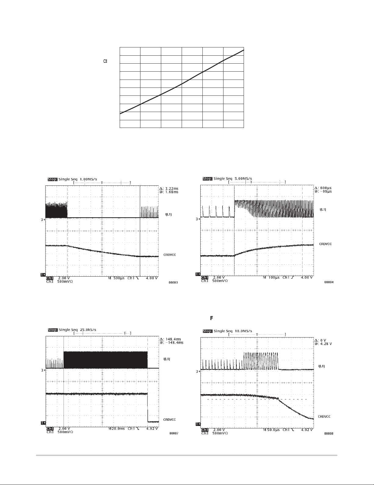
Figure 15. Transition from 5V to 3V Card Supply Figure 16. Transition from 3V to 5V Card Supply
95
Figure 17. Overcurrent Shutoff (t
=160ms)
d
http://onsemi.com
7
Figure 18. Undervoltage Shutoff (V
T5L
=4.6 V)
CS
PWRON
INT
RDYMOD
VBAT
240 k
240 k
VBAT
240 k
VBAT
240 k
VBATOK
MC33560
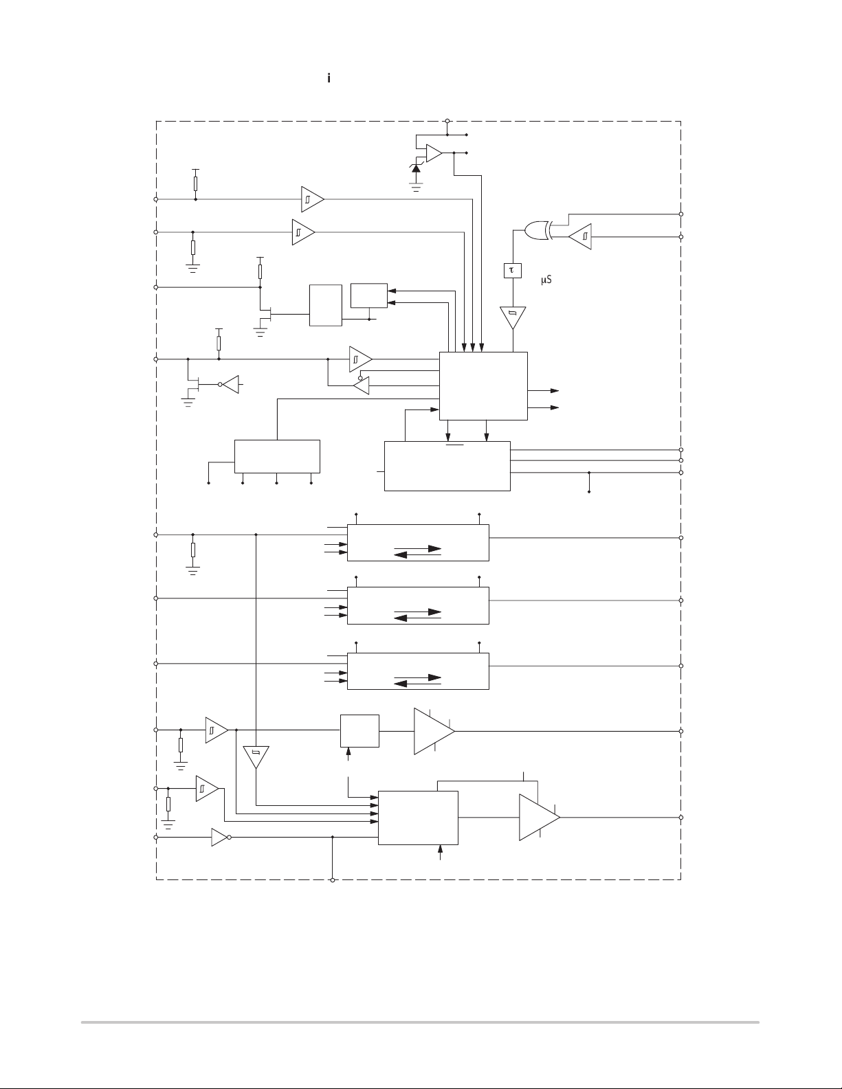
Figure 19. Functional Block Diagram
VBAT
VBAT
VBATOK
CS
PWRON
CS
CARD
CRDVCC
POWER
MANAGEMENT
LOGIC AND
PROGRAMMING
FAUL T
S
Q
LOGIC
R
CRDCON
CRDDET
DELAY
t
50 mS
PROGRAM
CARDENABLE
RESET
SYNCLK
ASYCLKIN
C4
C8
CARD PINS
SEQUENCER
SEQ2 SEQ3 SEQ4
SEQ1
VBAT
IO
240 k
SEQ1
CARDENABLE
VBATOK
VBAT
SEQ3
CARDENABLE
VBATOK
VBAT
SEQ3
CARDENABLE
VBATOK
DATA
LATCH
240 k
CARDENABLE
240 k
FAULT ON/OFF 3V/5V
VBAT
DC/DC CONVERTER
BIDIRECTIONAL
I/O
BIDIRECTIONAL
I/O
BIDIRECTIONAL
I/O
CLOCK
GENERATOR
AND
PROGRAMMING
VBAT
LEVEL
SHIFT
SEQ4
CRDVCC
CRDVCC
CRDVCC
CRDVCC
VBAT
LEVEL
SHIFT
CRDVCC
CRDVCC
ILIM
L1
CRDVCC
CRDIO
CRDC4
CRDC8
CRDRST
CRDCLK
SEQ2
INVOUT
PROGRAM
http://onsemi.com
8

MC33560
Table 1: PIN FUNCTION DESCRIPTION
Pin Symbol Type Name/Function
CONTROLLER INTERFACE
2 PWRON INPUT
pull down
3 INT OUTPUT
pull up
4 RDYMOD I/O & pull up This bidirectional pin has tri–state output and schmitt trigger input.
5 CS INPUT pull up This is the MC33560 chip select signal. Pins 2, 6, 7, 10, 20, 21 are disabled when CS=H. When
6 RESET INPUT
pull down
7 IO I/O This pin connects to the Serial I/O port of a microcontroller. A bi–directional level translator
8 INVOUT CLK
OUTPUT
9 ASYCLKIN CLK INPUT
high impedance
10 SYNCLK CLK INPUT
pull down
20 C8 I/O General purpose input/output. It has the same behavior as I/O, except for programming. It can
21 C4 I/O General purpose input/output. It has the same behaviour as I/O, except for programming. It
CARD INTERFACE
11 CRDIO I/O This pin connects to the serial I/O pin of the card connector. A bidirectional level translator
14 CRDRST OUTPUT This pin connects to the RESET pin of the card connector. A level translator adapts the
15 CRDCLK OUTPUT This pin connects to the CLK pin of the card connector. The CRDCLK signal is the output of
16 CRDC4 I/O General purpose input/output. It has the same behavior as CRDIO. It can be connected to the
17 CRDDET INPUT high
impedance
This pin is used to start operation of the internal DC/DC converter.
In programming mode, this pin is used to set the ”Output Voltage” switch. (see table 2).
This open collector pin indicates a change in the card presence circuit status. When a card is
inserted or extracted, the pin goes to logic level ”0”. The signal is reset to logic level ”1” upon
the rising edge of CS
application, two or more INT
poll all the MC33560s to identify which slot was detected.
* When RDYMOD is forced to 0, the MC33560 can be set to programming mode by a
negative transition on CS
* When RDYMOD is connected to a high impedance, the MC33560 is in normal operating
mode, and RDYMOD is in output mode (see tables 2 and 4):
– With CS
– With CS
RDYMOD=L, the MC33560 enters programming mode upon the falling edge of CS
20)
The signal present at this input pin is translated to pin 14 (the card reset signal) when CS=L.
The signal on this pin is latched when CS
table 2).
adapts the serial I/O signal between the smartcard and the microcontroller. The level
translator is enabled when CS
used in programming mode. (see table 2)
The ASYCLKIN (pin 9) signal is buffered and inverted to generate the output signal INVOUT.
This output is used for multislot applications, where the ASYCLKIN inputs and INVOUT
outputs are daisy–chained (see the multislot application example in figure 33).
This pin can be connected to the microcontroller master clock or any clock signal for
asynchronous cards. The signal is fed to the internal clock selector circuit, and is translated to
CRDCLK at the same frequency, or divided by 2 or 4, depending on programming (see table
3).
This function is used for communication with synchronous cards, and the pin is generally
connected to the controller serial interface clock signal. The signal is fed to the internal clock
selector circuit, and is translated to CRDCLK upon appropriate programming of the MC33560
(see table 3). When selected at programming, the signal on this pin is latched when CS
be connected to abidirectional port of the microcontroller. The level translator is en abled
when CS=L, and the signal is latched whenCS=H. (compare with pin 19)
can be connected to a bidirectional port of the microcontroller. The level translator is enabled
when CS
adapts the serial I/O signal between the card and the microcontroller (compare with pin 7)
RESET signal driven by the microcontroller (compare with pin 6).
the clock selector circuit.The clock selection is programmed using pins 2, 6 and 7 with
RDYMOD forced to ”0”.
C4 pin of the card connector.
This pin connects to the card detection switch of the card connector. Card detection phase is
determined with pin 18. This pin needs an external pull–up or pull–down resistor to operate
properly.
=L and PWRON=H, RDYMOD indicates the status of the DC/DC converter.
=L and PWRON=L, RDYMOD indicates the status of the card detector.
=L, and the signal is latched when CS=H. (compare with pin 16)
or upon the rising edge of PWRON. In the case of a multislot
outputs are connected together and the microcontroller has to
.
(see figure
=H. This pin is also used in programming mode (see
=L. The signal on thispin is latched when CS=H. This pin is also
=H.
http://onsemi.com
9

MC33560
Pin Name/FunctionTypeSymbol
CARD INTERFACE
18 CRDCON INPUT high
impedance
19 CRDC8 I/O General purpose input/output. It has the same behavior as CRDIO. It can be connected to the
CURRENT LIMIT AND THERMAL PROTECTION
1 PGND POWER This pin is the return path for the current flowing into pin 22 (L1). It must be connected to
12 CRDGND POWER This pin is the signal ground. It must be connected to the ground pin of the card connector. It
13 CRDVCC POWER This pin connects to the V
22 L1 POWER This pin connects to an external inductance for the DC/DC converter. Please refer to the
23 VBAT POWER This pin is connected to the supply voltage. Logic level ”1” of pins 2 to 10, 17, 18, 20 and 21 is
24 ILIM POWER This pin can be connected to the PGND pin, or to a resistor connected to PGND, or left open,
This pin connects to PGND or VBAT, or possibly to an output port of the microcontroller. With
this pin set to a logic “0”, the presence of a card is signalled with a logic ”1” on pin 17. With
this pin set to a logic ”1”, the presence of a card is signalled with a logic ”0” on pin 17.
C8 pin of the card connector
CRDGND using appropriate grounding techniques.
is the reference level for all analog and digital signals.
pin of the card connector. It is the reference level for a logic ”1”
of pins 11, 14, 15, 16 and 19.
description of the DC/DC converter functional block.
referenced to V
minimum value.
depending on the peak coil current needed to supply the card.
BAT
CC
. Operation of the MC33560 is inhibited when V
is lower than the
BAT
PROGRAMMING AND STATUS FUNCTIONS
The MC33560 features a programming interface and a status interface. Figure 20 shows how to enter and exit programming
mode; table 2 shows which pins are used to access the various functions.
Figure 20. MC33560 Programming Sequence
RDYMOD (in)
CS
PWRON
RESET
IO
ENTER
PROGRAMMING
MODE
Table 2: PIN USE FOR PROGRAMMING AND STATUS FUNCTIONS
Programs
CRDVCC
TO 3V/5V
RDYMOD
(in/out)
CS (in) rising edge 0 rising edge rising edge 0 0
PWRON 0/1 0/1 Programs CRDVCC Programs CRDVCC 0 or Hi–z 1
RESET (in) Programs CLK
IO (in) Programs CLK
Force to 0 READ Force to 0 Force to 0 READ READ
input/divide ratio
input/divide ratio
Select VCC
ON/OFF
NOT USED 0/1 0/1 NOT USED NOT USED
NOT USED 0/1 0/1 NOT USED NOT USED
PROGRAM DATA VALUE
PROGRAM DATA VALUE
PROGRAM DATA VALUE
Select
Clock Input
LATCH
PROGRAM
VALUE
Program ASYCLKIN
Divide Ratio
PROGRAMMING
EXIT
MODE
Poll Card
Status
Poll CRDVCC
Status
http://onsemi.com
10

MC33560
CARD VCC AND CARD CLOCK PROGRAMMING
The CRDV
frequency and to select 3V or 5V CRDV
options. The default power reset condition is state 4 (synchronous clock and CRDV
output variable in programming mode at the positive transition of CS (see figure 20).
Table 3 : CARD VCC AND CARD CLOCK TRUTH TABLE
STATE# PWRON RESET IO CRDVCC CRDCLK
Note : Card clock integrity is maintained during all frequency commutations (no spikes).
State 4 is the default state at power on.
DC/DC CONVERTER AND CARD DETECTOR STA TUS
The MC33560 status can be polled when
significance of the status message is described in table 4.
and ASYCLK programming options allow the system clock frequency to be matched to the card clock
CC
0 L L L 3V SYNCLK
1 L L H 3V ASYCLKIN/4
2 L H H 3V ASYCLKIN/2
3 L H L 3V ASYCLKIN
4 H L L 5V SYNCLK
5 H L H 5V ASYCLKIN/4
6 H H H 5V ASYCLKIN/2
7 H H L 5V ASYCLKIN
supply. Table 3 shows the values of PWRON, RESET and IO for the possible
CC
CS=L. Please consult table 2 for a description of input and output signals.The
=5V). All states are latched for each
CC
Table 4 : RDYMOD STATUS MESSAGES
PWRON
(input)
LOW LOW No card
LOW HIGH Card present
HIGH LOW DC/DC converter overload
HIGH HIGH DC/DC converter OK
RDYMOD
(output)
Message
http://onsemi.com
11

MC33560
DET AILED OPERATING DESCRIPTION
INTRODUCTION
The MC33560 smartcard interface IC has been designed
to provide all necessary functions for safe data transfers
between a microcontroller and a smartcard or memory card.
A card detector scans for the presence of a card and
generates a debounced wake–up signal to the
microcontroller.
Communication and control signal levels are translated
between the digital interface and the card interface by the
voltage level translator, and the card clock is matched to the
system clock frequency by the programmable card clock
Figure 21. MC33560 Operating Modes
CS: FALLING EDGE
STAND BY MODE
CS = H
PWRON = L
RDYMOD: 0 AND
CS: FALLING EDGE
RDYMOD: RISING EDGE
PROGRAMMING MODE
CS = L
RDYMOD = L
OPERATING MODES
CS: RISING EDGE
CS: 1 AND
ACTIVE MODE
CS = L
PWRON = L
CS: 0 AND
PWRON: RISING EDGE
ISO START SEQUENCE
The MC33560 has five operating modes:
⋅ stand by
⋅ programming
⋅ active
⋅ transaction
⋅ idle
The transitions between these different states are shown in
figure 21 above.
STAND BY MODE
Stand by mode allows the MC33560 to detect card
insertion and monitor the power supply while keeping the
power consumption at a minimum. It is obtained with CS
=H
and PWRON=L.
When the MC33560 detects a card, INT is asserted low to
wake up the Microcontroller.
PROGRAMMING MODE
The programming mode allows the user to configure the
card V
and the card clock signal for his specific
cc
application. The card supply , CRDVcc, can be programmed
to 3V or 5V, and the card clock signal can be defined to be
either synchronous, or asynchronous divided by 1, 2 or 4.
Programming mode is obtained with RDYMOD=L
followed by a negative transition on CS
. The programming
options are shown in table 3. Programmed values are latched
on a positive transition of CS
ACTIVE MODE
with RDYMOD=L.
In active mode, the MC33560 is selected, the RDYMOD
pin becomes an output, and the MC33560 status can be
polled. Power is not applied to the card.
generator. The power management unit enables the DC/DC
converter for card power supply, supervises the power
up/down sequence of the card’s I/O and signal lines, and
keeps the power consumption very low in stand by mode.
All card interface pins have adequate ESD protection, and
fault monitoring (V
BATlow
, V
CClow
, I
CClim
) guarantees
hazard–free card reader operation.
Several MC33560s can be operated in parallel, using the
same control and data bus, through the use of the chip select
signal
CS.
ERROR
ISO STOP SEQUENCE
PWRON: FALLING EDGE
OR ERROR CONDITION
TRANSACTION MODE
CS = L
PWRON = H
CONDITION
IDLE MODE
CS = H
PWRON = H
RDYMOD: 0 AND
CS: FALLING EDGE
RDYMOD: RISING EDGE
PROGRAMMING MODE
CS = L
RDYMOD = L
CS: 1 AND
The microcontroller polls the MC33560 by asserting
CS=L and reading the RDYMOD pin.
If a card is present, the microcontroller starts the DC/DC
converter by asserting PWRON=H. This starts the
automatic power on sequence: when CRDV
undervoltage level (V
T5H
or V
T3H
reaches the
cc
, depending on
programming), the card sequencer validates CRDIO,
CRDRST, CRDCLK, CRDC4, CRDC8 pins according to
the ISO7816–3 sequence (see figure 26). The MC33560 is
now in transaction mode, and the system is ready for data
exchange via the three I/O lines and the RESET
TRANSACTION MODE
line.
In transaction mode, the MC33560 maintains power and
the selected clock signal applied to the card, and the levels
of the IO, RESET, C4
and C8 signals between the
microcontroller and the card are translated depending on the
supply voltages V
BAT
and V
CC
.
The DC/DC converter status can be monitored on the
RDYMOD pin.
IDLE MODE
Idle mode is used when maintaining a card powered up
without communicating with it. When an asynchronous
clock is used, the selected clock signal is applied to the card
POWER DOWN OPERATION
Power–down can be initiated by the controlling
microprocessor, by stopping the DC/DC converter with
PWRON=L while CS=L, or by the MC33560 itself when
an error condition has been detected (CRDV
undervoltage,
cc
overcurrent longer than 160ms typ., overtemperature, “hot”
http://onsemi.com
12

MC33560
card extraction). The communication session is terminated
in a given sequence defined in ISO7816–3.
The MC33560 then goes into active mode, in which its
status can be polled.
Stand by mode is reached by deselecting the MC33560
(CS=H).
FUNCTIONAL BLOCKS
CARD DETECTOR
This block monitors the card contact CRDDET (during
insertion and extraction), filters the incoming waveform and
generates an interrupt signal INT
after each change. In order
to identify which coupler activated the INT line
(multicoupler application) the microcontroller scans both
circuits via CS and reads the RDYMOD pin.
The programming input CRDCON tells the level detector
which type of mechanical contact is implemented (normally
open or normally closed). Special care is taken to hold the
current consumption very low on this part of the circuit
which is continuously powered by the VBAT supply.
The CRDDET
pin has high impedance input, and an
external resistor must be connected to pull–up or pull– down,
depending on CRDCON. This resistor is chosen according to
the maximum leakage current of the card connector and the
PCB.
The card detector has an internal 50µs debouncing delay .
The micro controller has to insert an additional delay (in the
ms range) to allow the card contacts to stabilize in the card
connector before setting PWRON
=H.
When the card detector circuit detects a card extraction, it
activates the power–down sequence and stops the converter,
regardless of the PWRON
signal. The 50µs delay of the
debouncer is enough to ensure that all card signals have
reached a safe value before communication with the card
takes place.
CARD STATUS
The controlling microprocessor is informed of the
MC33560 status by interrupt and by polling. When a card is
extracted or inserted, the INT line is asserted low. The
interrupt is cleared upon the rising edge of CS
or upon the
rising edge of PWRON (INT line set to high state).
The microprocessor can poll the status at any time by
reading the RDYMOD pin with proper PWRON setting
(see tables 2 and 4 ).
Since INT
resistor (240k
and RDYMOD have a high value pull–up
W
typ.), their rise time can be as long as 10µs
if parasitic capacitance is high and no other pull–up circuitry
is connected.
POWER MANAGER
The task of the power manager is to activate only those
circuit functions which are needed for a determined operating
mode in order to minimize power consumption (see figure
19).
In stand by mode (PWRON=L) the power manager keeps
only the ”card present” detector alive. All card interface pins
are forced to ground potential.
In the event of a power–up request from the
microcontroller
(PWRON L to H transition, CS=L) the
power manager starts the DC/DC converter. As soon as the
CRDVCC supply reaches the operating voltage range, the
circuit activates the card signals in the following sequence:
CRDVCC, CRDIO, CRDCLK, CRDC4/C8, CRDRST
At the end of the transaction
(PWRON reset to L, CS=L)
or forced card extraction, the CRDVCC supply powers
down and the card signal deactivation sequence takes place:
CRDRST, CRDC4/C8, CRDCLK, CRDIO, CRDVCC
When CS
=L, the bi–directional signal lines (IO, C4 and
C8) are put into high impedance state to avoid signal
collision with the microcontroller in transmission mode.
BATTERY UNDERVOLTAGE DETECTOR
The task of this block is to monitor the supply voltage, and
to allow operation of the DC/DC converter only with valid
voltage (typically 1.5 V). The comparator has been designed
to have stability better than 20mV in the temperature range.
DC/DC CONVERTER
Upon request from the power manager, the DC/DC
converter generates the CRDVCC supply for the smartcard.
The output voltage is programmable for 3V or 5V (see table
3) to guarantee full cross compatibility of the reader for 5V
and 3V smartcards. The wide voltage supply range, 1.8V <
V
< 6.6V, accommodates a broad range of coupler
BAT
applications with different battery configurations (single
cell or multiple cells, serial or parallel connections).
The CRDVCC is current–limited and
short–circuit–proof.To avoid excessive battery loading
during a card short–circuit, a current integration function
forces the power–down sequence (see figure 28). To retry
the session, the microprocessor works through the power on
sequence as defined in the power manager section.
DC/DC Converter operating principles
The DC/DC converter architecture used in the MC33560
allows step–up and step–down voltage conversion to be
done. The unique regulation architecture permits an
automatic transition from step–up to step–down, and from
zero to full load, without affecting the output characteristics.
DC/DC Converter Description: The converter
architecture is very similar to the boost architecture, with an
active rectifier in place of the diode. The switching transistor
is connected to ground through a resistor network in order to
adjust the maximum peak current (see figure 22). A transistor
connected to the converter output
(CRDVCC) forces this pin
to a low voltage when the converter is not operating. This
prevents erratic voltage supply to the smartcard when not in
use.
http://onsemi.com
13

MC33560
The MC33560 has a built in oscillator; the DC/DC
converter requires only one inductor and the output filtering
capacitor to operate.
Step–Up Operation: When the card supply voltage is
lower than the battery voltage, the converter operates like a
boost converter; the active rectifier behavior is similar to
that of a diode.
Step–Down Operation: When the card supply voltage is
higher than the battery voltage, the rectifier control circuit
puts the power rectifying transistor in conduction when the
L1 voltage reaches V
BA T+VFSA T22
. The voltage across the
rectifying transistor is higher than in step–up operation. The
efficiency is lower, and similar to a linear regulator.
Figure 22. DC/DC Converter Functional Block
VBAT
L1
PWN
FEED
CLOCK OFF STOP
BACK
ILIMCOMP
DIGITAL
FILTER
ON /OFF
ON /OFF
OVER TEMP
DETECTION
–
+
LOGIC
AND
COUNTER
Low Side
Switch
120 mV
2
W
PGND ILIM
VBATOK
CONVERTER
FAULT
Fault Detection: The DC/DC converter has several
features that help to avoid electrical overstress of the
MC33560 and of the smartcard, and help to ensure that data
transmission with the smartcard occurs only when its supply
voltage is within predetermined limits. These functions are:
⋅ overtemperature detection,
⋅ current limitation, and
⋅ card supply undervoltage detection.
The level at which current will be limited is defined by the
maximum card supply current programmed with the
external components L1 and RLIM.
The undervoltage detection levels for 3V and 5V card
supply are preset internally to the MC33560.
Rectifier Switch CRDVCC
Active pull–down
switch
RECTIFIER
CONTROL
Internal
0.5
W
resistors
RLIM (external)
–
UNDER VOLTAGE
+
+
ERROR
AMP.
–
CRDGND
DETECTOR
VREF
ON /OFF
3V/5V
CRDGND
ON /OFF
The overcurrent and undervoltage protection features are
complementary, and will shut the circuit off either if the
overcurrent is high enough to bring the CRDVCC output
below the preset threshold, either after 160ms (typ.)
In addition, the DC/DC converter will be allowed to start
only if the battery supply voltage is high enough to allow
normal operation (1.8V).
The undervoltage comparator has a hysteresis and a delay
of typically 20ms to ensure stable operation. The current
detector is a comparator associated with two resistors: one
2W attached to PGND
and usually connected to analog
ground, and a 0.5W attached to ILIM, usually connected to
ground through an external resistor to adjust the maximum
peak current. The voltage developed across this resistor
network is then compared to a 120mV (typical) reference
voltage, and the comparator output performs a
cycle–by–cycle peak current limitation by switching off the
low side transistor when the voltage exceeds 120 mV.
The internal
ILIMCOMP signal is monitored to stop the
converter if current limitation is continuously detected
http://onsemi.com
during 160ms (typical). This allows normal operation with
high filtering capacitance and low peak current, even at
converter start–up. As a result, a short circuit to ground on
the card connector or a continuous overcurrent is reported by
RDYMOD 160ms (typical) after power up.
Unexpected card extraction: The MC33560 detects card
extraction and runs a power down sequence if card power is
still on when extraction occurs. An active pull–down switch
clamps CRDVCC to GND within 150µs (max) after
extraction is detected. The external capacitors will then be
discharged. With typical capacitor values of 10µF and 47nF
as indicated in the application schematic, the time needed to
discharge CRDVCC to a voltage below 0.4V can be
estimated to less than 750µs. The total time aftercard
extraction detection until CRDVCC reaches 0.4V is then
estimated to 900µs (max). All smartcard connector contacts
will be deactivated before CRDVCC deactivation. This
ensures that no electrical damage will be caused to the
smartcard under abnormal extraction conditions.
14

MC33560
3V/5V programming: It is possible to set the card supply
voltage to 3V or 5V at any time, before DC/DC converter
start, or during converter operation. When switching from
3V to 5V, a 160ms (typical) delay blanks the undervoltage
fault detection to allow filter capacitor charging.
PWM: The free–running integrated oscillator has two
working modes:
⋅ variable on–state and fixed frequency (typically
120KHz) for average to heavy loads.
⋅ variable on–state and variable frequency for light loads.
The frequency can be as low as a few kHz if no load is
connected to CRDVCC.
The charging current of the timing capacitor is related to
the V
supply voltage, to allow better line regulation, and
BA T
to increase stability.
Filtering Capacitor: A high value allows efficient
filtering of card current spikes. Low values allow low
start–up charging current. Care must be taken not to
combine low capacitor value with high current limiting, as
this can generate high ripple. Usual values range from 4.7µF
to 47µF, depending on current limiting.
Selecting the external components L1 and RLIM: The
choice of inductor L1 and resistor R4 is made by using figure
8 (5V card) and/or figure 9 (3V card) on page 8:
First, determine the maximum current that the application
requires to supply to the card (ICCmax, on the y–axis)
Then, select one curve that crosses the selected ICCmax
level. The curve is associated with an inductance value
(22µH, 47µH, or 100µH).
Finally , use the intersection of the curve and the ICCmax
level to find the Rlim value on the x–axis.
Good starting values are : L1
=47µH; R
lim
=0.5
W
Note also that, for a high inductance value (100µH), the
filtering capacitor is generally charged before inductance
current reaches current limitation, while for alow inductance
value, the current limitation is activated after a few converter
cycles.
Battery requirements: Having determined the L
R
values, the maximum current drawn from the battery
lim
1
and
supply is shown by the curves in figures 6 and 7.
When the application is powered by a single 3V battery,
special care has to be taken to extend its lifetime. When
lithium batteries approach the end–of–life, their internal
resistance increases, while voltage decreases. This
phenomenon can prevent the start–up of the DC/DC
converter if the current limiting is set too high, because of the
filtering capacitor charging current.
CLOCK GENERA T OR
The primary purpose of the clock generator module is to
match the smartcard operating frequency to the system
frequency. The source frequency can be provided to
ASYCLKIN by the microcontroller itself or from an
external oscillator circuit.
In programming mode
(RDYMOD=L and CS asserted
low) the three input variables PWRON, IO and RESET are
used to configure the two output variables CRDVCC and
CRDCLK as described in table 3. This circuit setup is
latched during the positive transition of CS
.
Furthermore, in asynchronous mode the system clock
frequency ASYCLKIN can be divided by a factor of 1, 2 or
4. The circuit controls the frequency commutation to
guarantee that the card clock signal remains free from spikes
and glitches. In addition, this circuit ensures that CRDCLK
signal pulses will not be shorter than the shortest and/or
longer than the longest of the clock signals present before
and after programming changes .
The INVOUT
output is provided to drive other circuits
without additional load to the microprocessor quartz
oscillator. It can also be used to build a local RC oscillator.
This driver has been optimized for low consumption; it has
no hysteresis, and input levels are not symmetrical. If the
ASYCLKIN pin is connected to a sine wave, the duty cycle
will not always be 50% at INVOUT.
Clock generator operating principles
Synchronous Clock: This clock is used mainly for
memory cards. It can also be used for asynchronous
(microprocessor) cards, allowing the use of two different
clock sources. The status of
SYNCLK is latched at CRDCLK
when CS goes high, so that data (the IO pin) and clock are
always consistent at the card connector, whatever the CS
status is. When using the synchronous clock, the clock
output becomes active only when the MC33560 is selected
with CS.
Asynchronous Clock: This clock is used mainly for
microprocessor cards. When applied, the clock output
remains active even when the MC33560 is not selected with
CS
, in order to keep the microprocessor running and avoid
an unwanted reset. The ASYCLKIN signal is buffered at the
INVOUT pin, so that several MC33560 systems can use the
same clock with one load only .
Depending on programming, the frequency is fed directly ,
or divided by 2 or by 4 to the CRDCLK
pin. If the duty cycle
of the applied clock signal is not exactly symmetrical, it is
recommended that the clock signal be divided by two or four
to guarantee 50% duty cycle.
Clock Signal Synchronization and Consistency (see
figure 29). The clock divider includes synchronization logic
that controls the switch from synchronous clock to
asynchronous (and vice–versa), from any division ratio to
any other ratio, during CS
changes and at power up. The
synchronization logic guarantees that each clock cycle on
the CRDCLK pin is finished before changing clock
selection (and has always the adequate duration), regardless
of the moment the programming is changed.
At power–up, when ASYCLKIN
is selected, the clock
signal at the CRDCLK pin has an entire length, according
to the selected divide ratio, whatever the ASYCLKIN signal
is versus the internal sequencer timing.
http://onsemi.com
15

MC33560
CARDENABLE
Figure 23. Clock Generator Functional Block
SYNCLK
CARDENABLE
ASYCLKIN
INVOUT
RESET
IO
LATCH
2
B
2
B
BIDIRECTIONAL LEVEL TRANSLATOR
This module (used on IO/CRDIO, C4/CRDC4,
C8/CRDC8, see figure 24) adapts the signal voltage levels
of the I/O and control lines between the micro controller
(supplied by V
) and the smartcard (supplied by
BAT
CRDVCC)
When CS
is low , with CRDVCC on, and start sequencing
completed, this module is transparent for the data, and acts
as if the card was directly connected to the reader
microcontroller. The core of the level shifter circuit defined
for the bidirectional CRDIO, CRDC4
and CRDC8 lines
consists of a NMOS switch which can be driven to the logic
low state from either side (microcontroller or card). If both
sides work in transmission mode with opposite phase, then
signal collision on the line is not avoidable. In this case, the
peak current is limited to a safe value for the integrated
circuit and the smartcard.
During high–to–low transitions, the NMOS transistor
impedance (T1=250W max.) is low enough to charge
parasitic capacitance, and have a high enough dv/dt. On low
to high transition, the NMOS transistor is not active above
a certain voltage, and an acceleration circuit is activated to
ensure a high dv/dt.
When the chip is disabled
(CS=H) with the voltage supply
CRDVCC still active, the IO, C4 and C8 lines keep their last
logic state.
When the converter is off, a transistor forces the CRDIO,
CRDC4 and CRDC8 lines to a low state, thus preventing
any unwanted voltage level to be applied to the data lines
when the card is not in use.
Figure 24. Bidirectional Translator Functional Block
IO
(C4)
(C8)
VBAT
CONTROL
LOGIC
SEQ1 (SEQ3)
T1
CRDVCC
T2
CRDGND
18 K
CRDIO
(CRDC4)
(CRDC8)
CRDVCC
SELECTOR
SYNCHRO
LATCH
SEQ3
CRDCLK
LOGIC
SYNCHRONISATION
SELECTOR
LATCH
PROGRAM
SECURITY FEATURES
The MC33560 has a number of unique security functions
to guarantee that no electrical damage will be caused to the
smartcard:
⋅ Battery supply minimum voltage threshold
⋅ Card supply undervoltage and overcurrent detection
with automatic shutdown
⋅ Card pin overvoltage clamp to CRDVCC
⋅ Card presence detector for ”clean” and fast shut–down
⋅ Consistent card signal sequencing at start–up and
power–down, according to ISO7816, even on error
conditions
⋅ Consistent clock signal, even when division ratio or
synchronization clock signal are changed ”on the fly” during
a card session (see figure 29)
⋅ Active pull–down on all card pins, including
CRDVCC, when not in normal operating mode.
A current limiting function and an overtemperature
detector are limiting power dissipation.
ESD PROTECTION
Due to the nature of smartcards, the card interface pins
must absorb high ESD (Electro Static Discharge) energy
during card insertion. In addition, the control circuits
attached to these pins must safely withstand short circuits
and voltage transients during forced card extraction.
Therefore, the MC33560 features enhanced ESD
protection, current limitation and short circuit protection on
all smartcard interface pins, including C4
and C8.
P ARALLEL OPERATION
For applications where two or more MC33560 are used,
the digital control and data bus lines are common to all
MC33560. Only the chip select signal, CS
, requires a
separate line for each interface.
While deselected, all communication pins except
CRDCLK will keep their logical state on the card side, and
will go to high impedance mode on the microprocessor side.
Figure 33 shows a typical application of a dual card reader.
This arrangement was chosen only to illustrate the parallel
operation of two card interfaces in the same module. The
discrete capacitor components are necessary to provide low
http://onsemi.com
16

MC33560
impedance on the supply lines VBA T and CRDVCC and to
suppress the high frequency noise due to the DC/DC
converter. The load resistors are external in order to adapt
the sense current of the ”cardpresent” switches.
MINIMUM POWER CONSUMPTION
CONSIDERATIONS
All analog blocks except the V
comparator and the
BAT
card presence detector are disabled in stand by mode
(CS
=H: DC/DC converter stopped).
Figure 25. Example of single sided PCB layout for MC33560
C8
C4
L1
VBAT
ILIM
PGND
C10
PWRON
R4 C6 C7
INT
RDYMOD
CS
In order to maintain stand by current at a minimum value,
all pins with pull–up resistance
(CS, INT, RDYMOD) have
to be kept in the high state or left open, and pins with
pull–down resistance
(RESET, SYNCLK, PWRON) have
to be kept in the low state or left open. ASYCLKIN should
not be connected to an active clock signal during stand by to
avoid dynamic currents. This is valid also for SYNCLK,
except that it can be left open.
CRDC8
CRDDET
CRDC4
CRDCLK
CRDRST
CRDVCC
CRDGND
SYNCLK
ASYCLKIN
INVOUT
IO
RESET
CRDIO
http://onsemi.com
17

CRDVCC
CS
MC33560
Figure 26. Card Signal Sequence During VCC Power Up/Down
POWER UP POWER DOWNNORMAL OPERATION
V
TxH
RDYMOD (out)
PWRON
CLK
C4. C8
RESET
CRDIO
CRDCLK
CRDC4, CRDC8
CRDRST
t
won
IO
t
tr
SEQ1 to SEQ4
SEQ4 to SEQ1
CRDDET
INT
CS
RDYMOD (out)
t
fltin
CS
to INT
15 mS typ.
INTERRUPT
SERVICING
Figure 27. Interrupt Servicing and Polling
t
fltout
t
drdy
POLLING
INTERRUPT
SERVICING
http://onsemi.com
18
POLLING

MC33560
Figure 28. Card Signal Sequence During VCC Overload and Unexpected Card Extraction
MCU deactivates PWRON
after card extraction
poll with PWRON = L –>
RDYMOD = H: card still present
CS
= L, PWRON = H
CRDVCC undervoltage
CRDVCC
card inserted
–> RDYMOD = L
t
fltin
overload time
smaller than t
(glitch not to scale)
dres
V
V
TxH
TxL
t
fltout
CRDDET
INT
CS
RDYMOD
PWRON
t
drdy
poll with PWRON = L –> RDYMOD = H:
card present
t
dres
MCU polls
RDYMOD = H
t
dres
greater than t
converter stop and
CRDVCC pull down
35 ns typ
overload time
dres
card extraction
poll with PWRON = H –> RDYMOD = L:
DC/DC converter overload
–>
http://onsemi.com
19

MC33560
Figure 29. ”On–the–fly” Card Clock Selection Examples
CS
RDYMOD
IO
RESET
ASYCLK
SYNCLK
CRDCLK
http://onsemi.com
20
CS
RDYMOD
IO
RESET
ASYCLK
SYNCLK
CRDCLK

http://onsemi.com
21
C5
10 uF
C1
Connector
DB9
10 uF
Q1: XTAL 4MHz
D1: General Purpose diode
R1: 47 kOhm
C1, C2, C4,C5: 10 uF
R2: 1 MOhm
C3: 220 nF
L1: MURATA LQH3C 47 uH
R3: 1 MOhm
C6: 200 nF
C7: 10 uF
C8, C9: 22 pF
M1: 7805 regulator
R4: Value depending on max. card current
Z1: General Purpose 40 V zener diode
U4: Card connector
U3
+
+
C2+
GND
C2–
VSS
RX1
TX1
RX2
TX2
RX3
TX3
MC145407
C1+
VCC
C1–
VDD
DO1
DI 1
DO2
DI 2
DO3
DI 3
M1
0.1 uF
R2
1M
C10
7805
Card Slot
U4
8..40 VDC
Z1
Card Detect
C8
C4
CLK
RST
VCC
GND
I/O
Figure 30. Card Reader/Writer Application
MC33560
47k
D1
R1
C4
10 uF
+
C reset
m
C2
10 uF
C3
220 nF
RESET
VDD
IRQ
0SC1
VPP
OSC2
NC
TCAP
PA7
PD7
PA6
NC
PA5
TCMP
PA4
SS
PA3
SCLK
PA2
MOSI
PA1
MISO
PA0
RDI
PB0
TDO
PB1
PC0
PB2
PC1
PB3
PC2
NC
PC3
PB4
PC4
PB5
PC5
PB6
PC6
PB7
PC7
VSS
NC
MC68HC705C9
U1
C8
22 pF
Q1
4 MHz
C9
R3
22 pF
1M
U2
MC33560
1 – PGND
2 – PWRON
3 –
INT
4 – RDYMOD
5 –
CS
6 – RESET
7 – IO
8 – INVOUT
9 – ASYCLKIN
10 – SYNCLK
11 – CRDIO
12 – CRDGND
R4*
ILIM – 24
VBAT – 23
L1 – 22
C4 – 21
C8 – 20
CRDC8 – 19
CRDCON – 18
CRDDET – 17
CRDC4 – 16
CRDCLK – 15
CRDRST – 14
CRDVCC – 13
L1
47 uH
C7
10 uFC6200 nF

MC33560
Figure 31. Multi Slot Card Reader/Writer Application
C8
C8
Card Detect
VBAT
C4
CLK
RST
VCC
GND
I/O
VBAT
Card Detect
C4
CLK
RST
VCC
GND
I/O
ILIM – 24
1 – PGND
MC33560
L1 – 22
C4 – 21
VBAT – 23
INT
2 – PWRON
3 –
4 – RDYMOD
C8 – 20
CRDC8 – 19
CRDCON – 18
CS
5 –
6 – RESET
7 – IO
CRDC4 – 16
CRDCLK – 15
CRDDET – 17
8 – INVOUT
9 – ASYCLKIN
10 – SYNCLK
VDD
0SC1
TCAP
OSC2
RESET
IRQ
VPPNCPA7
CRDRST – 14
CRDVCC – 13
11 – CRDIO
12 – CRDGND
NC
PD7
TCMP
PA6
PA5
SS
PA4
SCLK
PA3
MOSI
PA2
MISO
PA1
RDI
PA0
TDO
PB0
PC0
PB1
MC33560
PC1
PC2
PB2
PB3NCPB4
ILIM – 24
1 – PGND
PC3
PC4
L1 – 22
VBAT – 23
INT
2 – PWRON
3 –
PC5
PC6
PC7
PB5
PB6
PB7
C4 – 21
C8 – 20
CRDC8 – 19
CRDCON – 18
CS
4 – RDYMOD
5 –
6 – RESET
7 – IO
NC
MC68HC705
VSS
CRDC4 – 16
CRDCLK – 15
CRDDET – 17
8 – INVOUT
9 – ASYCLKIN
10 – SYNCLK
CRDRST – 14
CRDVCC – 13
11 – CRDIO
12 – CRDGND
C reset
m
VBAT
http://onsemi.com
22

U0.15 (0.006) T
U0.15 (0.006) T
–T–
S
L
S
0.10 (0.004)
SEATING
PLANE
2X L/2
PIN 1
IDENT.
D
MC33560
P ACKAGE DIMENSIONS
(TSSOP–24)
DTB SUFFIX
PLASTIC PACKAGE
CASE 948H–01
ISSUE O
24X REFK
0.10 (0.004) V
24
1
M
A
–V–
C
G
S
U
T
S
NOTES:
1. DIMENSIONING AND TOLERANCING PER ANSI
Y14.5M, 1982.
13
B
–U–
12
H
–W–
2. CONTROLLING DIMENSION: MILLIMETER.
3. DIMENSION A DOES NOT INCLUDE MOLD
FLASH, PROTRUSIONS OR GATE BURRS. MOLD
FLASH OR GATE BURRS SHALL NOT EXCEED 0.15
(0.006) PER SIDE.
4. DIMENSION B DOES NOT INCLUDE INTERLEAD
FLASH OR PROTRUSION. INTERLEAD FLASH OR
PROTRUSION SHALL NOT EXCEED
0.25 (0.010) PER SIDE.
5. DIMENSION K DOES NOT INCLUDE DAMBAR
PROTRUSION. ALLOWABLE DAMBAR
PROTRUSION SHALL BE 0.08 (0.003) TOTAL IN
EXCESS OF THE K DIMENSION AT MAXIMUM
MATERIAL CONDITION.
6. TERMINAL NUMBERS ARE SHOWN FOR
REFERENCE ONLY.
7. DIMENSION A AND B ARE TO BE DETERMINED
AT DATUM PLANE –W–.
DIM MIN MAX MIN MAX
A 7.70 7.90 0.303 0.311
B 4.30 4.50 0.169 0.177
C ––– 1.20 ––– 0.047
D 0.05 0.15 0.002 0.006
F 0.50 0.75 0.020 0.030
G 0.65 BSC 0.026 BSC
H 0.27 0.37 0.011 0.015
J 0.09 0.20 0.004 0.008
J1 0.09 0.16 0.004 0.006
K 0.19 0.30 0.007 0.012
K1 0.19 0.25 0.007 0.010
L 6.40 BSC 0.252 BSC
M 0 8 0 8
____
INCHESMILLIMETERS
DETAIL E
K
N
K1
J1
SECTION N–N
J
N
F
DETAIL E
0.25 (0.010)
M
http://onsemi.com
23

–T–
SEATING
PLANE
MC33560
P ACKAGE DIMENSIONS
(SO–24L)
DW SUFFIX
PLASTIC PACKAGE
CASE 751E–04
ISSUE E
–A–
1324
–B– P12X
M
0.010 (0.25) B
1
D24X
0.010 (0.25) B
M
T
12
J
S
A
S
M
F
R
C
M
22X
G
K
NOTES:
1. DIMENSIONING AND TOLERANCING PER ANSI
Y14.5M, 1982.
2. CONTROLLING DIMENSION: MILLIMETER.
3. DIMENSIONS A AND B DO NOT INCLUDE
MOLD PROTRUSION.
4. MAXIMUM MOLD PROTRUSION 0.15 (0.006)
PER SIDE.
5. DIMENSION D DOES NOT INCLUDE DAMBAR
PROTRUSION. ALLOWABLE DAMBAR
PROTRUSION SHALL BE 0.13 (0.005) TOTAL IN
EXCESS OF D DIMENSION AT MAXIMUM
MATERIAL CONDITION.
DIM MIN MAX MIN MAX
A 15.25 15.54 0.601 0.612
B 7.40 7.60 0.292 0.299
C 2.35 2.65 0.093 0.104
X 45
D 0.35 0.49 0.014 0.019
_
F 0.41 0.90 0.016 0.035
G 1.27 BSC 0.050 BSC
J 0.23 0.32 0.009 0.013
K 0.13 0.29 0.005 0.011
M 0 8 0 8
P 10.05 10.55 0.395 0.415
R 0.25 0.75 0.010 0.029
INCHESMILLIMETERS
____
ON Semiconductor and are trademarks of Semiconductor Components Industries, LLC (SCILLC). SCILLC reserves the right to make changes
without further notice to any products herein. SCILLC makes no warranty , representation or guarantee regarding the suitability of its products for any particular
purpose, nor does SCILLC assume any liability arising out of the application or use of any product or circuit, and specifically disclaims any and all liability ,
including without limitation special, consequential or incidental damages. “Typical” parameters which may be provided in SCILLC data sheets and/or
specifications can and do vary in different applications and actual performance may vary over time. All operating parameters, including “Typicals” must be
validated for each customer application by customer’s technical experts. SCILLC does not convey any license under its patent rights nor the rights of others.
SCILLC products are not designed, intended, or authorized for use as components in systems intended for surgical implant into the body, or other applications
intended to support or sustain life, or for any other application in which the failure of the SCILLC product could create a situation where personal injury or
death may occur. Should Buyer purchase or use SCILLC products for any such unintended or unauthorized application, Buyer shall indemnify and hold
SCILLC and its officers, employees, subsidiaries, affiliates, and distributors harmless against all claims, costs, damages, and expenses, and reasonable
attorney fees arising out of, directly or indirectly , any claim of personal injury or death associated with such unintended or unauthorized use, even if such claim
alleges that SCILLC was negligent regarding the design or manufacture of the part. SCILLC is an Equal Opportunity/Affirmative Action Employer .
PUBLICATION ORDERING INFORMATION
USA/EUROPE Literature Fulfillment:
Literature Distribution Center for ON Semiconductor
P.O. Box 5163, Denver, Colorado 80217 USA
Phone: 303–675–2175 or 800–344–3860 Toll Free USA/Canada
Fax: 303–675–2176 or 800–344–3867 Toll Free USA/Canada
Email: ONlit@hibbertco.com
Fax Response Line*: 303–675–2167
800–344–3810 Toll Free USA/Canada
*To receive a Fax of our publications
N. America Technical Support: 800–282–9855 Toll Free USA/Canada
http://onsemi.com
ASIA/PACIFIC: LDC for ON Semiconductor – Asia Support
Phone: 303–675–2121 (Tue–Fri 9:00am to 1:00pm, Hong Kong Time)
Email: ONlit–asia@hibbertco.com
JAPAN: ON Semiconductor, Japan Customer Focus Center
4–32–1 Nishi–Gotanda, Shinagawa–ku, T okyo, Japan 141–8549
Phone: 81–3–5487–8345
Email: r14153@onsemi.com
ON Semiconductor Website: http://onsemi.com
For additional information, please contact your local Sales Representative.
MC33560/D
24
 Loading...