

Order this document by MC33502/D
The MC33502 operational amplifier provides rail–to–rail operation on both
the input and output. The output can swing within 50 mV of each rail. This
rail–to–rail operation enables the user to make full use of the entire supply
voltage range available. It is designed to work at very low supply voltages
(1.0 V and ground), yet can operate with a supply of up to 7.0 V and ground.
Output current boosting techniques provide high output current capability
while keeping the drain current of the amplifier to a minimum.
• Low Voltage, Single Supply Operation (1.0 V and Ground to
7.0 V and Ground)
• High Input Impedance: Typically 40 fA Input Current
• Typical Unity Gain Bandwidth @ 5.0 V = 5.0 MHz, @ 1.0 V = 4.0 MHz
• High Output Current (I
• Output Voltage Swings within 50 mV of Both Rails @ 1.0 V
• Input Voltage Range Includes Both Supply Rails
• High Voltage Gain: 100 dB Typical @ 1.0 V
• No Phase Reversal on the Output for Over–Driven Input Signals
• Input Offset Trimmed to 0.5 mV Typical
• Low Supply Current (I
• 600 Ω Drive Capability
• Extended Operating Temperature Range (–40 to 105°C)
APPLICATIONS
• Single Cell NiCd/Ni MH Powered Systems
• Interface to DSP
• Portable Communication Devices
• Low Voltage Active Filters
• Telephone Circuits
• Instrumentation Amplifiers
• Audio Applications
• Power Supply Monitor and Control
• Compatible with VCX Logic
Inputs
= 50 mA @ 5.0 V, 10 mA @ 1.0 V)
SC
= 1.2 mA/per Amplifier, Typical)
D
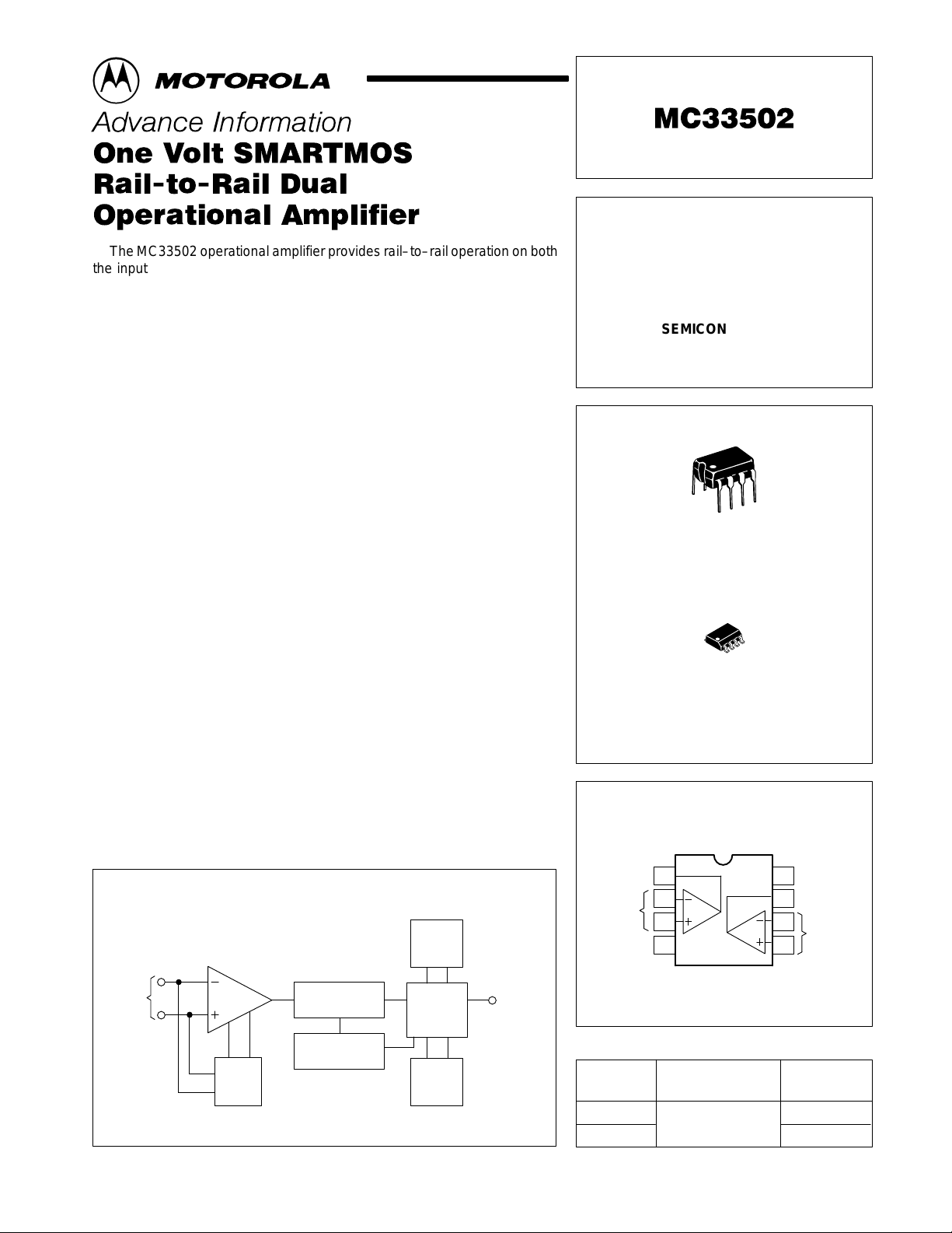
Simplified Block Diagram
Input
Stage
Buffer with 0 V
Level Shift
Base
Current
Boost
Output
Stage
Outputs
LOW VOLTAGE
RAIL–TO–RAIL DUAL
OPERATIONAL AMPLIFIER
SEMICONDUCTOR
TECHNICAL DATA
8
1
P SUFFIX
PLASTIC PACKAGE
CASE 626
8
1
D SUFFIX
PLASTIC PACKAGE
CASE 751
(SO–8)
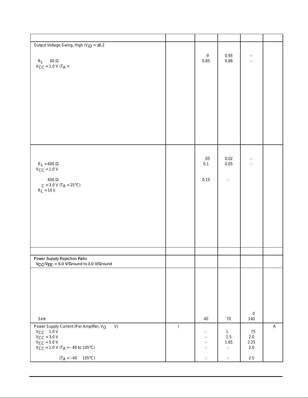
PIN CONNECTIONS
Output 1
Inputs 1
18
2
1
3
V
4
EE
(Dual, Top View)
2
V
CC
Output 2
7
6
Inputs 2
5
Saturation
Offset
Voltage
Trim
This device contains 98 active transistors per amplifier.
This document contains information on a new product. Specifications and information herein
are subject to change without notice.
MOTOROLA ANALOG IC DEVICE DATA
Detector
Base
Current
Boost
ORDERING INFORMATION
Operating
Device
MC33502P
MC33502D
Motorola, Inc. 1998 Rev 0
Temperature Range
TA = – 40° to +105°C
Package
Plastic DIP
SO–8
1
MAXIMUM RATINGS
ÁÁÁ
ÁÁÁ
ÁÁÁ
ÁÁÁ
ÁÁÁ
Rating Symbol Value Unit
Supply Voltage (VCC to VEE)
ESD Protection Voltage at any Pin
Human Body Model
MC33502
V
S
V
ESD
7.0
2000
V
V
Voltage at Any Device Pin
Input Differential Voltage Range
Common Mode Input Voltage Range
Output Short Circuit Duration
Maximum Junction Temperature
Storage Temperature Range
Maximum Power Dissipation
NOTES: 1. Power dissipation must be considered to ensure maximum junction temperature (TJ) is not
DC ELECTRICAL CHARACTERISTICS (V
exceeded.
2.ESD data available upon request.
CC
V
V
V
T
DP
IDR
CM
t
S
T
stg
P
J
D
VS ±0.3
VCC to V
VCC to V
(Note 1)
150
–65 to 150
(Note 1)
EE
EE
V
V
V
s
°C
°C
mW
= 5.0 V, VEE = 0 V, VCM = VO = VCC/2, RL to VCC/2, TA = 25°C, unless
otherwise noted.)
Characteristic
Input Offset Voltage (VCM = 0 to VCC)
Symbol Min Typ Max Unit
V
IO
VCC = 1.0 V
TA = 25°C –5.0 0.5 5.0
TA = –40° to 105°C –7.0 – 7.0
VCC = 3.0 V
TA = 25°C –5.0 0.5 5.0
TA = –40° to 105°C –7.0 – 7.0
VCC = 5.0 V
TA = 25°C –5.0 0.5 5.0
TA = –40° to 105°C –7.0 – 7.0
Input Offset Voltage Temperature Coefficient (RS = 50 Ω)
∆VIO/∆T
–
8.0
TA = –40° to 105°C
Input Bias Current (VCC = 1.0 to 5.0 V)
Common Mode Input Voltage Range
Large Signal Voltage Gain
I IIB I
V
ICR
A
VOL
–
V
EE
40
–
VCC = 1.0 V (TA = 25°C)
RL = 10 kΩ 25 100 –
RL = 1.0 kΩ 5.0 50 –
VCC = 3.0 V (TA = 25°C)
RL = 10 kΩ 50 500 –
RL = 1.0 kΩ 25 100 –
VCC = 5.0 V (TA = 25°C)
RL = 10 kΩ 50 500 –
RL = 1.0 kΩ 25 200 –
mV
–
–
V
CC
µV/°C
fA
V
kV/V
2
MOTOROLA ANALOG IC DEVICE DATA
MC33502
ÁÁÁ
ÁÁÁ
ÁÁÁ
ÁÁÁ
DC ELECTRICAL CHARACTERISTICS (continued) (V
= 5.0 V, VEE = 0 V, VCM = VO = VCC/2, RL to VCC/2, TA = 25°C, unless
CC
otherwise noted.)
Characteristic UnitMaxTypMinSymbol
Output Voltage Swing, High (VID = ±0.2 V)
V
OH
VCC = 1.0 V (TA = 25°C)
RL = 10 kΩ 0.9 0.95 –
RL = 600 Ω 0.85 0.88 –
VCC = 1.0 V (TA = –40° to 105°C)
RL = 10 kΩ 0.85 – –
RL = 600 Ω 0.8 – –
VCC = 3.0 V (TA = 25°C)
RL = 10 kΩ 2.9 2.93 –
RL = 600 Ω 2.8 2.84 –
VCC = 3.0 V (TA = –40° to 105°C)
RL = 10 kΩ 2.85 – –
RL = 600 Ω 2.75 – –
VCC = 5.0 V (TA = 25°C)
RL = 10 kΩ 4.9 4.92 –
RL = 600 Ω 4.75 4.81 –
VCC = 5.0 V (TA = –40° to 105°C)
RL = 10 kΩ 4.85 – –
RL = 600 Ω 4.7 – –
Output Voltage Swing, Low (VID = ±0.2 V)
V
OL
VCC = 1.0 V (TA = 25°C)
RL = 10 kΩ 0.05 0.02 –
RL = 600 Ω 0.1 0.05 –
VCC = 1.0 V (TA = –40° to 105°C)
RL = 10 kΩ 0.1 – –
RL = 600 Ω 0.15 – –
VCC = 3.0 V (TA = 25°C)
RL = 10 kΩ 0.05 0.02 –
RL = 600 Ω 0.1 0.08 –
VCC = 3.0 V (TA = –40° to 105°C)
RL = 10 kΩ 0.1 – –
RL = 600 Ω 0.15 – –
VCC = 5.0 V (TA = 25°C)
RL = 10 kΩ 0.05 0.02 –
RL = 600 Ω 0.15 0.1 –
VCC = 5.0 V (TA = –40° to 105°C)
RL = 10 kΩ 0.1 – –
RL = 600 Ω 0.2 – –
Common Mode Rejection (Vin = 0 to 5.0 V) CMR 60 75 – dB
V
OL
60
75
–
Output Short Circuit Current (Vin Diff = ±1.0 V)
I
SC
VCC = 1.0 V
Source 6.0 13 26
Sink 10 13 26
VCC = 3.0 V
Source 15 32 60
Sink 40 64 140
VCC = 5.0 V
Source 20 40 140
Sink 40 70 140
Power Supply Current (Per Amplifier, VO = 0 V)
I
D
VCC = 1.0 V – 1.2 1.75
VCC = 3.0 V – 1.5 2.0
VCC = 5.0 V – 1.65 2.25
VCC = 1.0 V (TA = –40 to 105°C) – – 2.0
VCC = 3.0 V (TA = –40 to 105°C) – – 2.25
VCC = 5.0 V (TA = –40 to 105°C) – – 2.5
V
V
µV/V
mA
mA
MOTOROLA ANALOG IC DEVICE DATA
3
MC33502
ÁÁÁ
ÁÁÁ
Á
Á
Á
Á
Á
ÁÁÁ
Á
Á
Á
Á
Á
Á
ÁÁÁ
Á
Á
Á
Á
Á
Á
ÁÁÁ
Á
Á
Á
Á
Á
Á
ÁÁÁ
Á
ÁÁÁ
ÁÁÁ
ÁÁÁ
ÁÁÁ
AC ELECTRICAL CHARACTERISTICS (V
Characteristic
Slew Rate (VS = ±2.5 V , VO = –2.0 to 2.0 V, RL = 2.0 kΩ, AV = 1.0)
= 5.0 V, VEE = 0 V, VCM = VO = VCC/2, TA = 25°C, unless otherwise noted.)
CC
Symbol Min Typ Max Unit
SR
Positive Slope 2.0 3.0 6.0
Negative Slope 2.0 3.0 6.0
Unity Gain Bandwidth
BW
VCC = 1.0 V 3.0 4.0 6.0
VCC = 3.0 V 3.5 4.5 7.0
VCC = 5.0 V 4.0 5.0 8.0
Gain Margin (RL =10 kΩ, CL = 0 pF)
БББББББББББББББББ
Phase Margin (RL = 10 kΩ, CL = 0 pF)
БББББББББББББББББ
Channel Separation (f = 1.0 Hz to 20 kHz, RL = 600 Ω)
БББББББББББББББББ
Power Bandwidth (VO = 4.0 Vpp, RL = 1.0 kΩ, THD ≤1.0%)
БББББББББББББББББ
Total Harmonic Distortion (VO = 4.5 Vpp, RL = 600 Ω, AV = 1.0)
Am
ÁÁÁ
φ
m
ÁÁÁ
CS
ÁÁÁ
BW
P
ÁÁÁ
THD
–
ÁÁ
–
ÁÁ
–
ÁÁ
–
ÁÁ
6.5
ÁÁ
60
ÁÁ
120
ÁÁ
200
ÁÁ
f = 1.0 kHz – 0.004 –
f = 10 kHz – 0.01 –
Differential Input Resistance (VCM = 0 V)
Differential Input Capacitance (VCM = 0 V)
Equivalent Input Noise Voltage (VCC = 1.0 V, VCM = 0 V, VEE = Gnd,
R
in
C
in
e
n
–
–
>1.0
2.0
RS = 100 Ω)
f = 1.0 kHz – 30 –
f = 10 kHz – 60 –
–
ÁÁ
–
ÁÁ
–
ÁÁ
–
ÁÁ
–
–
V/µs
MHz
dB
ÁÁ
Deg
ÁÁ
dB
ÁÁ
kHz
ÁÁ
%
terraΩ
pF
nV/√Hz
IN–
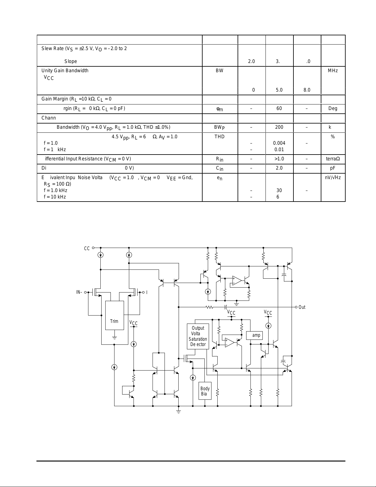
Figure 1. Representative Block Diagram
V
CC
IN+
Offset
Voltage
Trim
V
CC
V
CC
Output
Voltage
Saturation
Clamp
V
CC
Detector
Body
Bias
Out
4
MOTOROLA ANALOG IC DEVICE DATA

MC33502
GENERAL INFORMATION
The MC33502 dual operational amplifier is unique in its
ability to provide 1.0 V rail–to–rail performance on both the
input and output by using a SMARTMOS process. The
amplifier output swings within 50 mV of both rails and is able
to provide 50 mA of output drive current with a 5.0 V supply,
and 10 mA with a 1.0 V supply. A 5.0 MHz bandwidth and a
slew rate of 3.0 V/µs is achieved with high speed depletion
mode NMOS (DNMOS) and vertical PNP transistors. This
device is characterized over a temperature range of –40°C
to 105°C.
CIRCUIT INFORMATION
Input Stage
One volt rail–to–rail performance is achieved in the
MC33502 at the input by using a single pair of depletion
mode NMOS devices (DNMOS) to form a differential
amplifier with a very low input current of 40 fA. The normal
input common mode range of a DNMOS device, with an ion
implanted negative threshold, includes ground and relies on
the body effect to dynamically shift the threshold to a positive
value as the gates are moved from ground towards the
positive supply. Because the device is manufactured in a
p–well process, the body effect coefficient is sufficiently large
to ensure that the input stage will remain substantually
saturated when the inputs are at the positive rail. This also
applies at very low supply voltages. The 1.0 V rail–to–rail
input stage consists of a DNMOS differential amplifier, a
folded cascode, and a low voltage balanced mirror. The low
voltage cascoded balanced mirror provides high 1st stage
gain and base current cancellation without sacrificing signal
integrity . Also, the input of fset voltage is trimmed to less than
1.0 mV because of the limited available supply voltage. The
body voltage of the input DNMOS differential pair is internally
trimmed to minimize the input offset voltage. A common
mode feedback path is also employed to enable the offset
voltage to track over the input common mode voltage. The
total operational amplifier quiescent current drop is
1.3 mA/amp.
Output Stage
An additional feature of this device is an “on demand” base
current cancellation amplifier. This feature provides base
drive to the output power devices by making use of a buffer
amplifier to perform a voltage–to–current conversion. This is
done in direct proportion to the load conditions. This “on
demand” feature allows these amplifiers to consume only a
few micro–amps of current when the output stage is in its
quiescent mode. Yet it provides high output current when
required by the load. The rail–to–rail output stage current
boost circuit provides 50 mA of output current with a 5.0 V
supply (For a 1.0 V supply output stage will do 10 mA)
enabling the operational amplifier to drive a 600 Ω load. A
buffer is necessary to isolate the load current effects in the
output stage from the input stage. Because of the low voltage
conditions, a DNMOS follower is used to provide an
essentially zero voltage level shift. This buffer isolates any
load current changes on the output stage from loading the
input stage. A high speed vertical PNP transistor provides
excellent frequency performance while sourcing current. The
operational amplifier is also internally compensated to
provide a phase margin of 60 degrees. It has a unity gain of
5.0 MHz with a 5.0 V supply and 4.0 MHz with a 1.0 V supply .
LOW VOLTAGE OPERATION
The MC33502 will operate at supply voltages from 0.9 to
7.0 V and ground. When using the MC33502 at supply
voltages of less than 1.2 V, input offset voltage may
increase slightly as the input signal swings within
approximately 50 mV of the positive supply rail. This effect
occurs only for supply voltages below 1.2 V, due to the input
depletion mode MOSFETs starting to transition between the
saturated to linear region, and should be considered when
designing high side dc sensing applications operating at the
positive supply rail. Since the device is rail–to–rail on both
input and output, high dynamic range single battery cell
applications are now possible.
MOTOROLA ANALOG IC DEVICE DATA
5
 Loading...