Order this document by MC33470/D
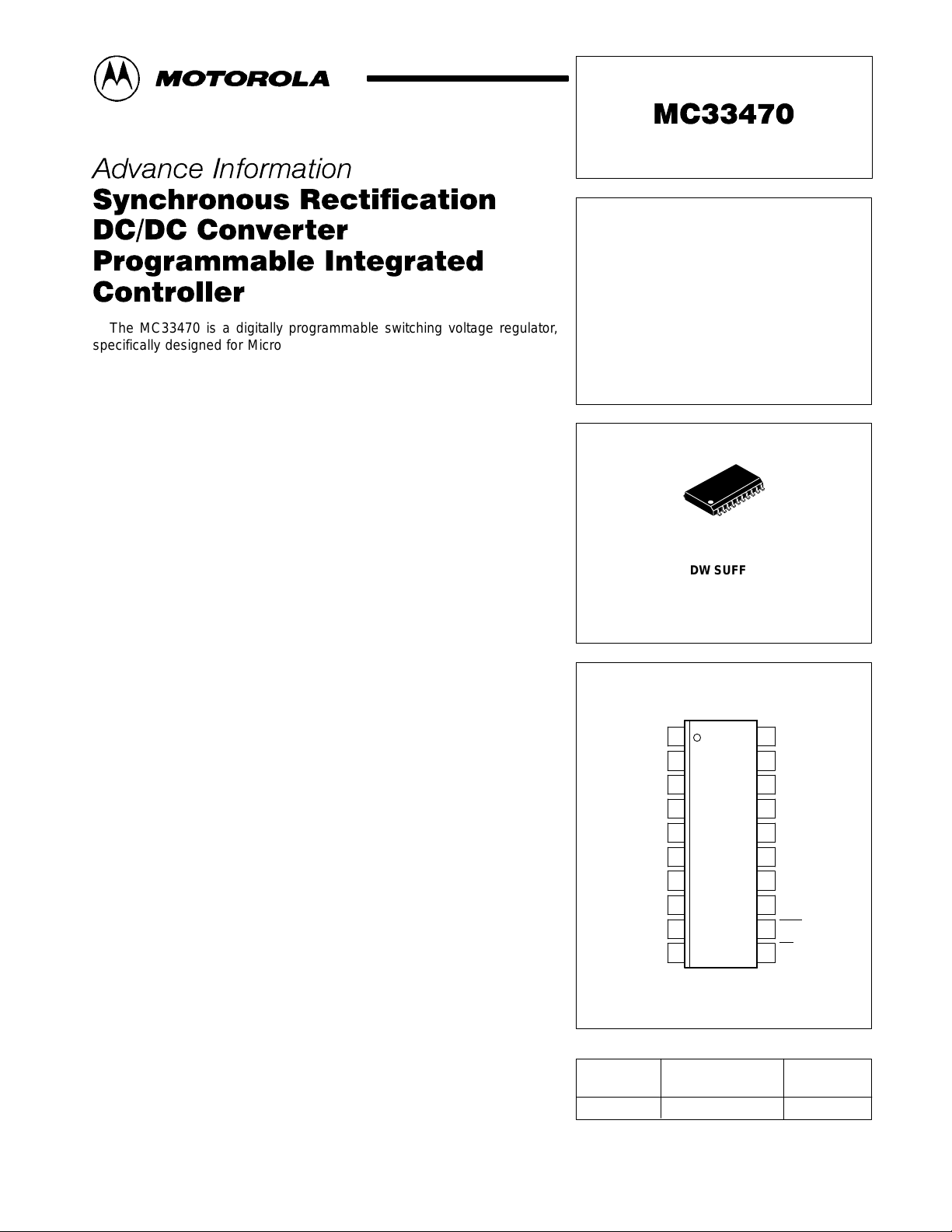
The MC33470 is a digitally programmable switching voltage regulator,
specifically designed for Microprocessor supply, Voltage Regulator Module
and general purpose applications, to provide a high power regulated output
voltage using a minimum of external parts. A 5–bit digital–to–analog converter
defines the dc output voltage.
This product has three additional features. The first is a pair of high speed
comparators which monitor the output voltage and expedite the circuit
response to load current changes. The second feature is a soft start circuit
which establishes a controlled response when input power is applied and
when recovering from external circuit fault conditions. The third feature is two
output drivers which provide synchronous rectification for optimum
efficiency.
This product is ideally suited for computer, consumer, and industrial
equipment where accuracy, efficiency and optimum regulation performance
is desirable.
MC33470 Features:
• 5–Bit Digital–to–Analog Converter Allows Digital Control of
Output Voltage
• High Speed Response to Transient Load Conditions
• Output Enable Pin Provides On/Off Control
• Programmable Soft Start Control
• High Current Output Drives for Synchronous Rectification
• Internally Trimmed Reference with Low Temperature Coefficient
• Programmable Overcurrent Protection
• Overvoltage Fault Indication
• Functionally Similar to the L TC1553
SYNCHRONOUS
RECTIFICATION DC/DC
CONVERTER
PROGRAMMABLE
INTEGRATED CONTROLLER
SEMICONDUCTOR
TECHNICAL DATA
20
1
DW SUFFIX
PLASTIC PACKAGE
CASE 751D
(SO–20L)
PIN CONNECTIONS
G2
P
V
CC
P
Gnd
A
Gnd
V
CC
Sense
I
max
I
fb
SS
Compensation
1
2
3
4
5
6
7
8
9
10
20
19
18
17
16
15
14
13
12
11
G1
OUTEN
VID0
VID1
VID2
VID3
VID4
P
wrgd
Fault
OT
This document contains information on a new product. Specifications and information herein
are subject to change without notice.
MOTOROLA ANALOG IC DEVICE DATA
(Top View)
ORDERING INFORMATION
Operating
Device
MC33470DW SO–20LTA = 0° to +75°C
Motorola, Inc. 1997 Rev 0
Temperature Range
Package
1
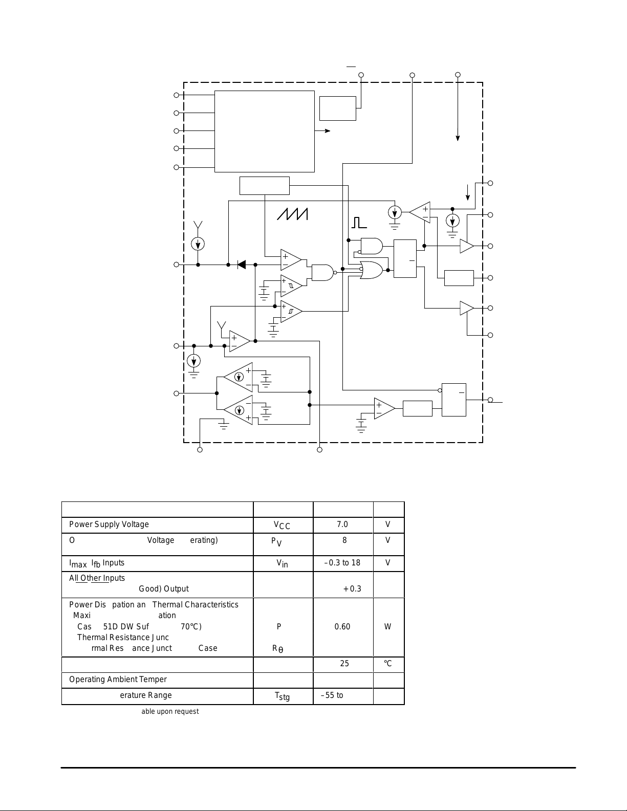
Voltage
Á
Á
Á
Á
Identification
Code
Input
Sense
Power
Good
MC33470
Simplified Block Diagram
18
VID0
17
VID1
16
VID2
15
VID3
14
VID4
V
CC
10
9
SS
6
20 µA
13
Digitally Programmed
Reference
Oscillator
µ
A
0.96 V
ref
V
ref
800
µ
OTA Error Amp
1.5 V
+
+
+
+
PWM
Comparator
1.04 V
ref
1.04 V
ref
0.93 V
ref
2.5 V
Over
Temp
V
ref
1.14 V
OT
ref
11
90
Outen
Over Current
µ
A
S
R
PWM
Latch
5
V
19
CC
V
CC
7
Detect
En
Q
Q
190 µA
Delay
I
2
P
20
G1
8
I
1
G2
3
P
R
Delay Fault
S
14
Q
max
V
CC
fb
Gnd
Compensation
MAXIMUM RATINGS (T
A
410
Gnd
= 25°C, unless otherwise noted.)
C
Rating Symbol Value Unit
Power Supply Voltage
Output Driver Supply Voltage (Operating)
ББББББББББББ
I
, Ifb Inputs
max
All Other Inputs and Digital
V
CC
P
V
ÁÁ
CC
V
in
V
in
ÁÁÁ
–0.3 to 18
–0.3 to
(OT, Fault, Power Good) Outputs VCC + 0.3
Power Dissipation and Thermal Characteristics
Maximum Power Dissipation
Case 751D DW Suffix (TA = 70°C)
Thermal Resistance Junction–to–Ambient
Thermal Resistance Junction–to–Case
Operating Junction Temperature
Operating Ambient Temperature (Notes 1 and 2)
Storage Temperature Range
NOTE: ESD data available upon request
R
R
T
P
θJA
θJC
T
T
stg
D
J
A
0 to +70
–55 to +125
7.0
18
0.60
91
60
125
V
V
Á
V
V
W
°C/W
°C/W
°C
°C
°C
2
MOTOROLA ANALOG IC DEVICE DATA
MC33470
ÁÁÁ
ÁÁÁ
ÁÁÁ
ÁÁÁ
ÁÁÁ
ÁÁÁ
ÁÁÁ
ÁÁÁ
ÁÁÁ
ÁÁÁ
ÁÁÁ
ÁÁÁ
ÁÁÁ
ÁÁÁ
ÁÁÁ
ÁÁÁ
ÁÁÁ
ÁÁÁ
ÁÁÁ
ÁÁÁ
ÁÁÁ
ÁÁÁ
ÁÁÁ
ÁÁÁ
ÁÁÁ
ÁÁÁ
ÁÁÁ
ÁÁÁ
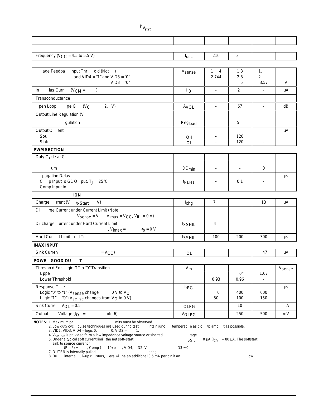
ELECTRICAL CHARACTERISTICS (V
min/max values TA is the operating ambient temperature range that applies, unless otherwise noted.)
Characteristic
= 5.0 V, P
CC
, = 12 V for typical values TA = Low to High [Notes 1, 2, 3], for
P
VCC
V
CC
Symbol Min Typ Max Unit
OSCILLAT OR
Frequency (VCC = 4.5 to 5.5 V)
f
osc
210
FEEDBACK AMPLIFIER
Voltage Feedback Input Threshold (Note 4)
VID0, VID1, VID2 and VID4 = “1” and VID3 = “0”
VID4 = “1” and VID0, VID1, VID2 and VID3 = “0”
Input Bias Current (VCM = 2.8 V)
Transconductance (VCM = 2.8 V, V
Open Loop Voltage Gain (V
COMP
COMP
= 2.0 V)
= 2.0 V)
Output Line Regulation (VCC = 4.5 to 5.5 V)
Output Load Regulation
V
sense
A
Reg
Reg
I
IB
G
M
VOL
load
line
1.764
2.744
3.43
–
400
–
–
–
Output Current
Source
Sink
I
I
OH
OL
–
–
PWM SECTION
Duty Cycle at G1 Output
Maximum
Minimum
DC
DC
max
min
77
–
Propagation Delay
Comp Input to G1 Output, TJ = 25°C
Comp Input to G2 Output, TJ = 25°C
t
PLH1
t
PLH2
–
–
SOFT–START SECTION
Charge Current (V
Soft–Start
Discharge Current under Current Limit (Note 5)
(V
Soft–Start
= 2.0 V, V
Discharge Current under Hard Current Limit
(V
Soft–Start
= 2.0 V, V
Hard Current Limit Hold Time
sense
sense
= 0 V)
= V
< V
out
out
, V
/2, V
imax
imax
= VCC, V
= VCC, V
ifb
ifb
= 0 V)
= 0 V)
I
chg
I
SSIL
I
SSHIL
t
SSHIL
7.0
30
40
100
IMAX INPUT
Sink Current (Vin
max
= VCC, V
= VCC)
ifb
I
OL
133
POWER GOOD OUTPUT
Threshold For Logic “1” to “0” Transition
Upper Threshold
Lower Threshold
Response Time
Logic “0” to “1” (V
Logic “1” to “0” (V
changes from 0 V to VO)
sense
changes from VO to 0 V)
sense
Sink Current (VOL = 0.5 V)
Output Low Voltage (IOL = 100 µA) (Note 6)
NOTES: 1. Maximum package power dissipation limits must be observed.
2.Low duty cycle pulse techniques are used during test to maintain junction temperature as close to ambient as possible.
3.VID1, VID3, VID4 = logic 0, and VID0, VID2 = logic 1.
4.V
5.Under a typical soft current limit, the net soft–start discharge current will be 90 µA (I
6 Sense (Pin 6) = 5.0 V, Comp (Pin 10) open, VID4, VID2, VID1, VID0 = 1.0, VID3 = 0.
7.OUTEN is internally pulled low if VID0, 1, 2, 3, and 4 are floating.
8.Due to internal pull–up resistors, there will be an additional 0.5 mA per pin if any of the VID0, 1, 2, 3, or 4 pins are pulled low.
is provided from a low impedance voltage source or shorted to the output voltage.
sense
sink to source current ratio is designed to be 9:1.
V
t
rPG
I
OLPG
V
OLPG
th
SSIL
) – 10 µA (I
–
0.93
200
50
–
–
chg
300
1.8
2.8
3.5
20
800
67
7.0
5.0
120
120
88
–
0.1
0.1
10
90
64
200
190
1.04
0.96
400
100
10
250
) = 80 µA. The softstart
390
1.836
2.856
3.57
–
1200
–
–
–
–
–
95
0
–
–
13
150
–
300
247
1.07
–
600
150
–
500
kHz
µA
µmho
dB
mV
mV
µA
µA
µA
mA
µA
V
sense
mA
mV
V
V
V
%
µs
µs
µs
MOTOROLA ANALOG IC DEVICE DATA
3
MC33470
ÁÁÁ
ÁÁÁ
ÁÁÁ
ÁÁÁ
ÁÁÁ
ÁÁÁ
ÁÁÁ
ÁÁÁ
ÁÁÁ
ÁÁÁ
ÁÁÁ
ÁÁÁ
ÁÁÁ
ÁÁÁ
ÁÁÁ
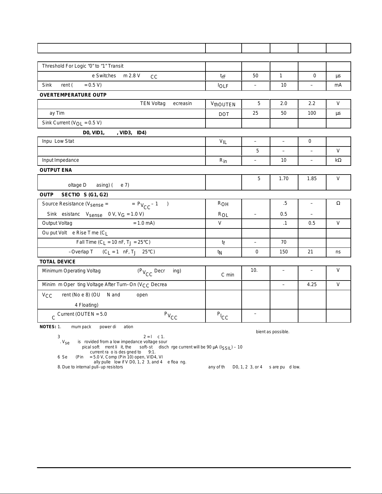
ELECTRICAL CHARACTERISTICS
min/max values TA is the operating ambient temperature range that applies, unless otherwise noted.)
(continued) (VCC = 5.0 V, P
, = 12 V for typical values TA = Low to High [Notes 1, 2, 3], for
P
VCC
V
CC
Characteristic UnitMaxTypMinSymbol
FAULT OUTPUT
Threshold For Logic “0” to “1” Transition
V
Response Time Switches from 2.8 V to V
sense
Sink Current (VOL = 0.5 V)
CC
V
t
I
OLF
thF
rF
1.12
50
–
OVERTEMPERATURE OUTPUT
Threshold For Logic “1” to “0” Transition (OUTEN V oltage Decreasing)
Delay Time
Sink Current (VOL = 0.5 V)
V
thOUTEN
t
DOT
I
OLF
1.85
25
–
LOGIC INPUTS (VID0, VID1, VID2, VID3, VID4)
Input Low State
Input High State
Input Impedance
V
IL
V
IH
R
in
–
3.5
–
OUTPUT ENABLE CONTROL (OUTEN)
Over–Temperature Driver Disable and Reset
V
OTDD
1.55
(OUTEN Voltage Decreasing) (Note 7)
OUTPUT SECTIONS (G1, G2)
= 1.0 mA)
sink
P
VCC
V
– 1.0 V)
CC
Source Resistance (V
Sink Resistance (V
= 2.0 V, VG = P
sense
= 0 V, VG = 1.0 V)
sense
Output Voltage with OUTEN Reset (I
Output Voltage Rise T ime (CL = 10 nF, TJ = 25°C)
Output Voltage Fall T ime (CL = 10 nF, TJ = 25°C)
G1, G2 Non–Overlap Time (CL = 10 nF, TJ = 25°C)
R
R
V
t
NOL
OH
OL
OL
t
r
t
f
– 0.5 – Ω
–
–
–
–
30
TOTAL DEVICE
Minimum Operating Voltage After Turn–On (P
P
VCC
V
CC
Decreasing)
Minimum Operating Voltage After Turn–On (VCC Decreasing)
VCC Current (Note 8) (OUTEN and P
P
VCC
V
CC
open,
P
V
CC min
VCC
I
min
CC
10.8 – – V
3.0
– 3.7 8.0 mA
VID0, 1, 2, 3, 4 Floating)
P
P
Current (OUTEN = 5.0 V, VID0, 1, 2, 3, 4 Open, P
VCC
V
CC
NOTES: 1. Maximum package power dissipation limits must be observed.
2.Low duty cycle pulse techniques are used during test to maintain junction temperature as close to ambient as possible.
3.VID1, VID3, VID4 = logic 0, and VID0, VID2 = logic 1.
4.V
5.Under a typical soft current limit, the net soft–start discharge current will be 90 µA (I
6 Sense (Pin 6) = 5.0 V, Comp (Pin 10) open, VID4, VID2, VID1, VID0 = 1.0, VID3 = 0.
7.OUTEN is internally pulled low if VID0, 1, 2, 3, and 4 are floating.
8.Due to internal pull–up resistors, there will be an additional 0.5 mA per pin if any of the VID0, 1, 2, 3, or 4 pins are pulled low.
is provided from a low impedance voltage source or shorted to the output voltage.
sense
sink to source current ratio is designed to be 9:1.
P
VCC
V
CC
= 12 V)
P
I
CC
SSIL
) – 10 µA (I
– 15 – mA
chg
1.14
100
10
2.0
50
10
–
–
10
1.70
0.5
0.1
70
70
150
–
) = 80 µA. The softstart
1.2
150
–
2.2
100
–
0.8
–
–
1.85
–
0.5
140
140
210
4.25
V
µs
mA
µs
mA
kΩ
ns
ns
ns
ref
V
V
V
V
V
V
4
MOTOROLA ANALOG IC DEVICE DATA
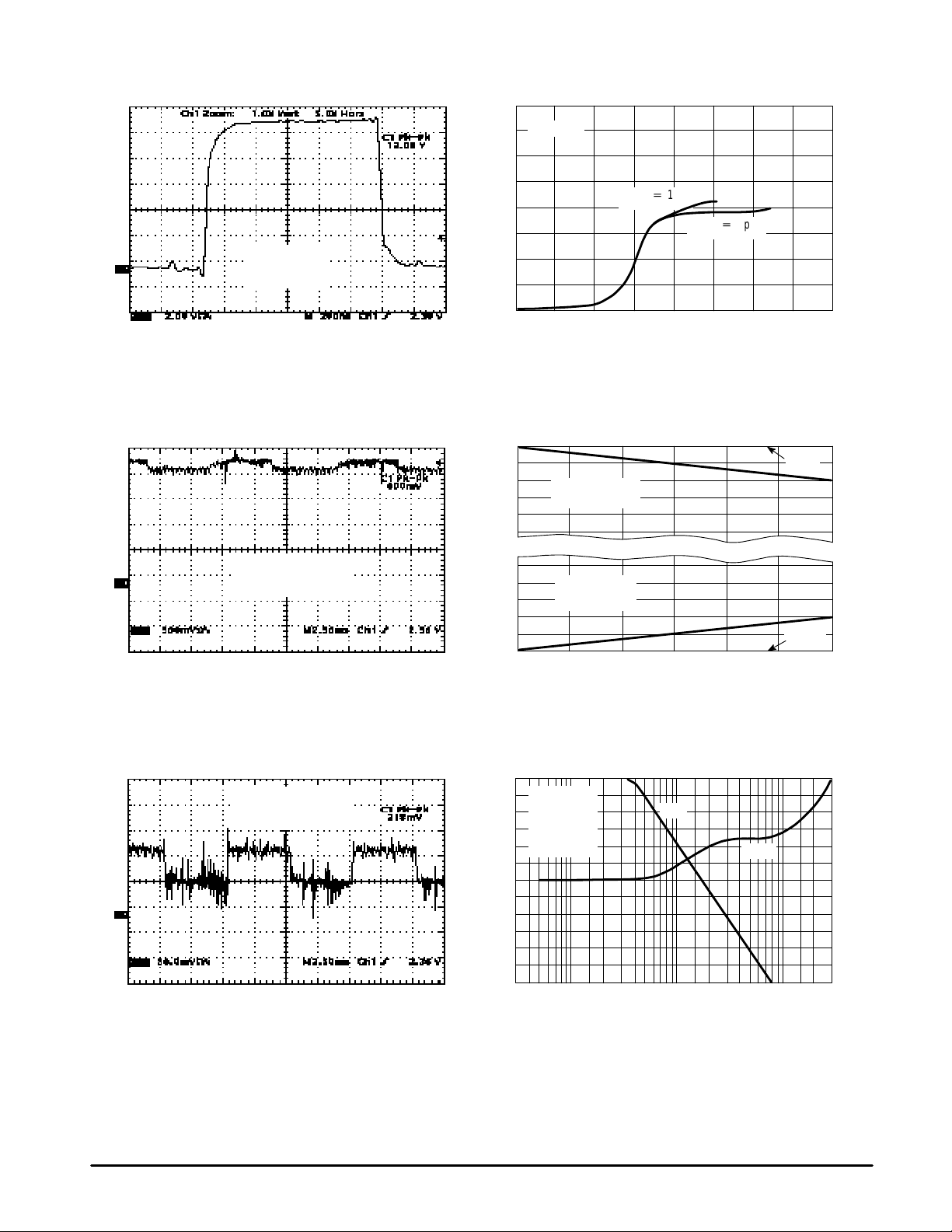
Figure 1. Output Drive Waveform Figure 2. 5.0 V Supply Current
2.0 V/DIV500 mV/DIV50 mV/DIV
VO = 2.8 V
IO = 3.3 A
Figure 13 Circuit
200 nS/DIV
Figure 3. Error Amplifier Transient Response
MC33470
8.0
7.0
6.0
5.0
4.0
3.0
, SUPPLY CURRENT (mA)
2.0
CC
I
1.0
0
0
–0.5
–1.0
TA = 25°C
P
+
12 V
V
CC
P
+
Open
V
CC
0 1.0 2.0 3.0 4.0 5.0 6.0
INPUT VOLTAGE (V)
7.0
Figure 4. Drive Output Source/Sink Saturation
V oltage versus Load Current
P
Source Saturation
(Load to Ground)
V
8.0
CC
VO = 2.8 V
0
IO transient = 0.3 to 16 A
Figure 13 Circuit
2.5 mS/DIV
1.0
0.5
0
Figure 5. Feedback Circuit Load
Transient Response
20
VO = 2.8 V
IO transient = 0.3 to 16 A
Figure 13 Circuit
2.5 mS/DIV
15
10
5.0
LOOP GAIN (dB)
0
–5.0
–10
300
Sink Saturation
(Load to P
0 0.2 0.4 0.6 0.8 1.0 1.2
)
V
CC
Ground
Figure 6. Feedback Loop Gain and Phase
versus Frequency
V
= 12 V
CCP
VCC = 5.0 V
VO = 2.8 V
IO = 3.3 A
°
C
TA = 25
1.0 k 10 k 100 k 300 k3.0 k 30 k
Gain
Phase
f, FREQUENCY (Hz)
0
30
60
90
120
, EXCESS PHASE (DEGREES)
∅
150
180
MOTOROLA ANALOG IC DEVICE DATA
5
 Loading...