MOTOROLA MC33468SN-20ATR Datasheet

ÁÁÁÁ
ÁÁÁÁ
ÁÁÁÁ
ÁÁÁÁ
ÁÁÁÁ
Order this document by MC33468/D
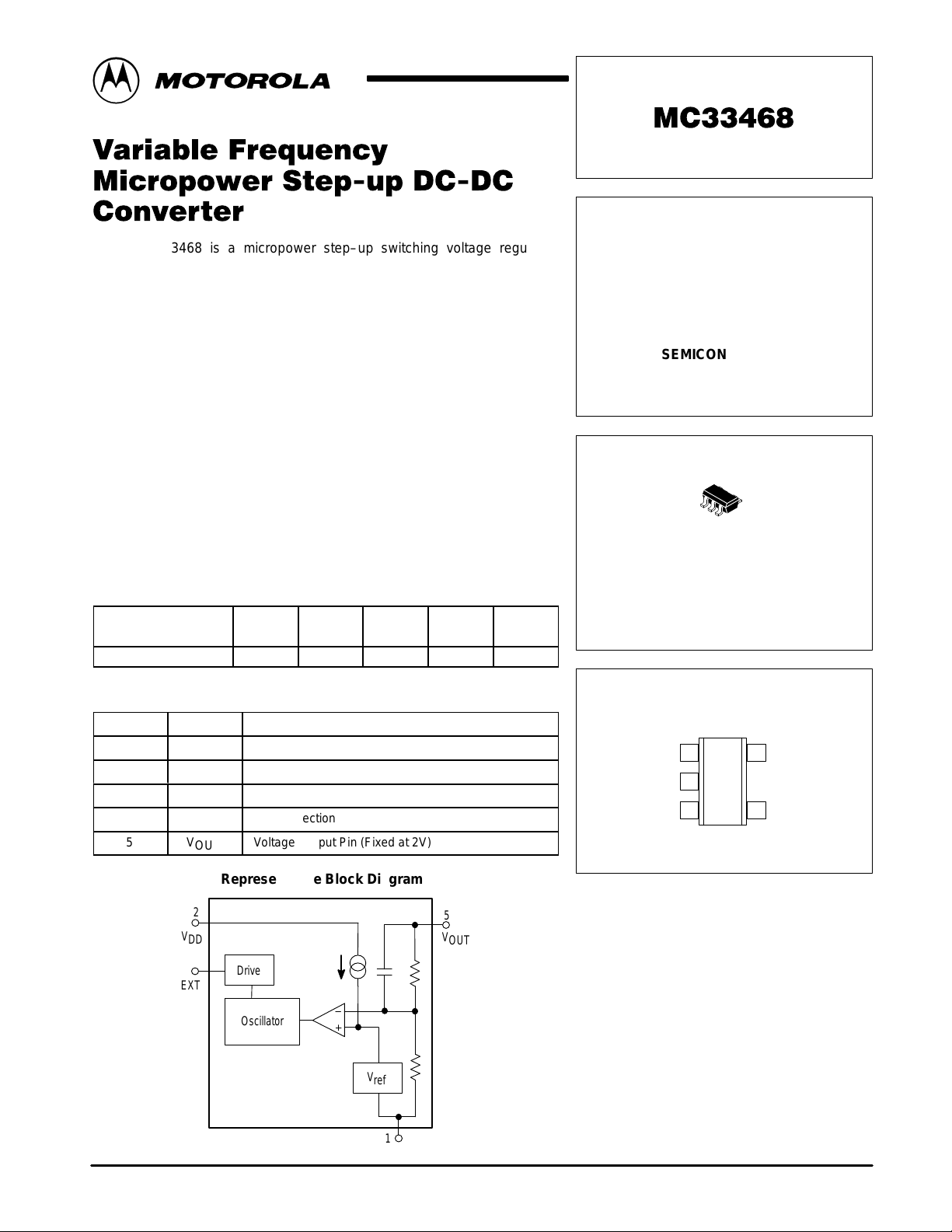
The MC33468 is a micropower step–up switching voltage regulator,
specifically designed for handheld and pager applications, to provide a
regulated output voltage using a minimum of external parts. This device
features a quiescent bias current of 3.0 µA typical.
The MC33468 features a highly accurate voltage reference, an error
amplifier, an oscillator, a variable frequency modulation (VFM) controller, a
drive pin (EXT) for an external transistor, and feedback resistors.
The Vout pin is fixed at 2V in the IC. The output of the converter with an
inductor, a diode, a capacitor, a drive transistor , and feed–back resistors can
have an output of 30V.
MC33468 Features:
• Low Quiescent Bias Current of 3.0 µA
• High Output Voltage Accuracy of ±2.5%
• Low Startup Voltage of 0.8 V at No Load
• Output Voltage Set With External Resistors
• Operating Temperature Range: –40°C to +85°C
• Surface Mount Package
ORDERING INFORMATION
Output
Device
MC33468SN–20ATR 2.0 0KXX* 7” 8 mm 3000
* “XX” denotes the lot number.
Voltage
Marking
PIN DESCRIPTION
Pin No. Symbol Description
1
2
3
4
5
GND
V
EXT
NC
V
OUT
DD
Ground
Input
External Transistor Drive
No Connection
Voltage Output Pin (Fixed at 2V)
Reel
Size
Tape
Width
Quantity
VARIABLE FREQUENCY
MICROPOWER DC–to–DC
CONVERTER
SEMICONDUCTOR
TECHNICAL DATA
5
1
N SUFFIX
PLASTIC PACKAGE
CASE 1212
(SOT–23–5)
PIN CONNECTIONS
15
Ground
Vdd
EXT
2
3
(Top View)
V
OUT
N/C
4
Representative Block Diagram
2
V
DD
3
EXT
Drive
Oscillator
MOTOROLA ANALOG IC DEVICE DATA
5
V
OUT
V
ref
Gnd
1
1

MC33468
Á
Á
Á
Á
Á
Á
Á
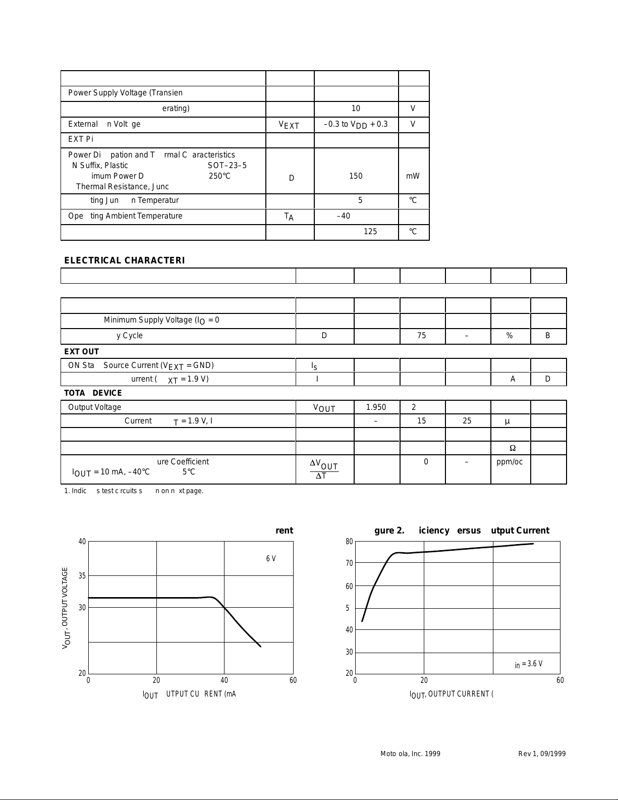
MAXIMUM RATINGS
Power Supply Voltage (Transient)
Power Supply Voltage (Operating)
External Pin Voltage
EXT Pin Source/Sink Current
(TC = 25°C, unless otherwise noted.)
Rating
Symbol Value Unit
V
V
V
I
DD
DD
EXT
EXT
Power Dissipation and Thermal Characteristics
N Suffix, Plastic Package Case 1212 (SOT–23–5)
Maximum Power Dissipation @ T
Thermal Resistance, Junction–to–Air R
Operating Junction Temperature
Operating Ambient Temperature
Storage Temperature Range
ELECTRICAL CHARACTERISTICS (V
= 250°C P
A
= 1.9 V, TA = 25°C, unless otherwise noted.)
DD
T
θJA
T
T
stg
Characteristic
OSCILLAT OR
Frequency
Oscillator Minimum Supply Voltage (IO = 0 mA)
Oscillator Duty Cycle
EXT OUTPUT
ON State Source Current (V
OFF State Sink Current (V
EXT
EXT
= GND)
= 1.9 V)
TOTAL DEVICE
Output Voltage
Quiescent Bias Current (V
Quiescent Bias Current (V
Internal Resistor (V
OUT
= 1.9 V, IO = 0 mA)
OUT
= 2.1 V, IO = 0 mA)
OUT
to GND)
Output Voltage Temperature Coefficient
I
= 10 mA, –40°C ≤ TA ≤ 85°C
OUT
БББББББББББББББ
1. Indicates test circuits shown on next page.
12
10
–0.3 to VDD + 0.3
50/50
D
150 mW
V
V
V
mA
667 °C/W
J
A
125
–40 to +85
–55 to +125
°C
°C
°C
Symbol Min Typ Max Unit Note
f
osc
V
DD
D
I
source
I
sink
V
OUT
I
Q
I
Q
R
Vout
D
V
OUT
D
T
ÁÁÁ
A
–
–
65
1.5
1.5
1.950
–
–
2.0
–
ÁÁ
180
0.7
75
–
–
2.000
15
3.0
–
±50
ÁÁ
–
0.8
–
–
–
2.050
25
5.0
–
–
ÁÁ
kHz
M
ppm/oc
ÁÁ
V
%
mA
mA
V
µA
µA
1
B
B
B
C
D
A
A
W
E
Á
Figure 1. Output Voltage versus Output Current
40
35
30
, OUTPUT VOL TAGE (V)
OUT
25
V
0
I
, OUTPUT CURRENT (mA)
OUT
2
Vin = 3.6 V
Figure 2. Efficiency versus Output Current
80
70
60
50
EFFICIENCY
40
30
2020
0
Motorola, Inc. 1999 Rev 1, 09/1999
Vin = 3.6 V
2020 4040 6060
I
, OUTPUT CURRENT (mA)
OUT
MOTOROLA ANALOG IC DEVICE DATA

MC33468
A
C
V
DD
GND
GND
V
V
OUT
OUT
A A
EXT
V
DD
EXT
B
Oscilloscope
D
V
DD
EXT
V
DD
EXT
GND
GND
V
OUT
V
OUT
E
V
DD
EXT
GND
V
OUT
A
Figure 3. T est Circuit Schematics
MOTOROLA ANALOG IC DEVICE DATA
3
 Loading...