

MOTOROLA MC33441DTBEL, MC33441DTBR2 Datasheet
Semiconductor Components Industries, LLC, 2000
April, 2000 – Rev. 1
1 Publication Order Number:
MC33441/D
MC33441
Electroluminescent Lamp
Driver IC
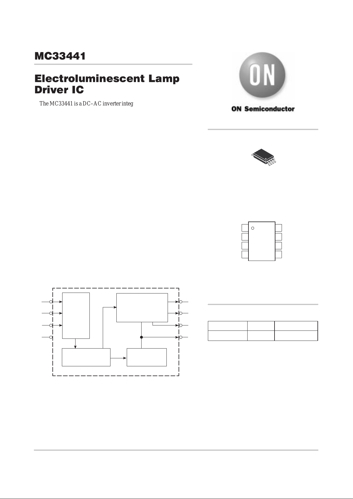
The MC33441 is a DC–AC inverter integrated circuit for driving EL
lamps. It can boost the supply voltage to the level required by EL
lamps and also provide high voltage AC lamp excitation. It consists of
an oscillator, a frequency divider , a coil driving circuit and a switched
H–bridge network. The input supply voltage range is from 1.8V to
3.5V and is capable to supply a typical 140Vpp AC output voltage.
The standby current of the device is typically 10nA which is ideal for
low power portable products. Externally, one inductor and one resistor
are needed to generate the desirable voltage charge and to fine tune the
oscillator’s frequency. This device is offered in 8–Pin TSSOP
miniature package. The operating temperature is –20°C to 70°C.
Features:
• Battery Operation 1.8V – 3.5V
• Typical Voltage Output 140Vpp
• Typical Standby Current 10nA
• Internal Oscillator with External Tuning Resistor
• Enable Control Pin with a 300K Internal Pull–Down Resistor
• 8–Pin TSSOP Package (Thickness = 1.05mm, Width = 4.5mm,
Length = 3.1mm & Lead Pitch = 0.65mm)
Types of Applications:
• Pagers, Cellular Phones, Portable CD Players/Minidisks
• Databanks, Calculators
Simplified Block Diagram
FREQUENCY
DIVIDER
VDD
ENB
RT1
OSC
F
EL
VSS
1
2
3
4
H–BRIDGE
COIL
DRIVER
F
COIL
EL1
EL2
FILTER
COIL
8
7
6
5
Device Package Shipping
ORDERING INFORMATION
MC33441DTBR2 TSSOP–8 2500 Units / Reel
TSSOP–8
DTB SUFFIX
CASE 948J
http://onsemi.com
8
1
PIN CONNECTIONS AND
MARKING DIAGRAM
4
3
VSS COIL
FILTER
5
6
(Top View)
ENB
RT1
1
VDD
EL2
EL1
7
8
2
M33
441
ALY
W
A = Assembly Location
L = Wafer Lot
Y = Y ear
W = Work Week
MC33441
http://onsemi.com
2
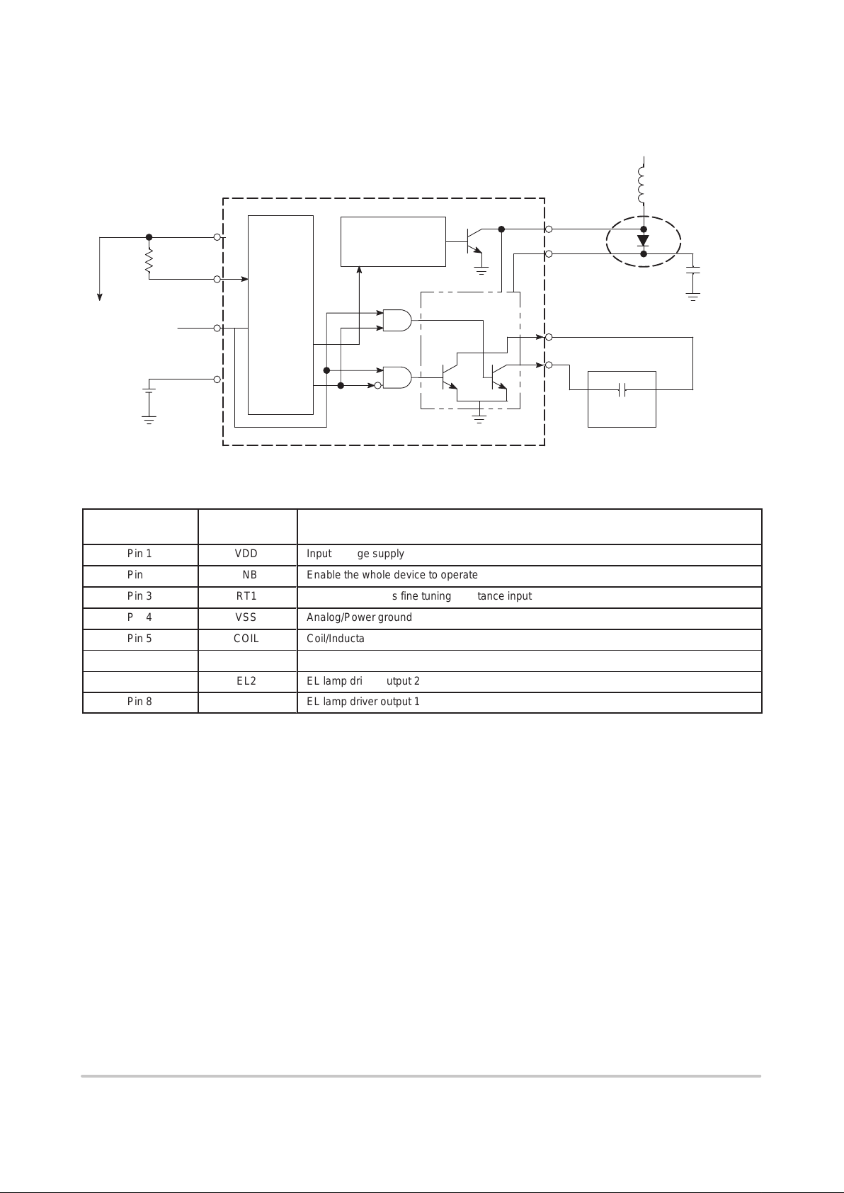
Figure 1. Test Circuit
H–BRIDGE
VSS
ENB
RT1
OSC
&
FREQ.
DIVIDER
F
EL
VDD
1
2
3
4
COIL DRIVER
EL LAMP
AND2
EL1
EL2
FILTER
COIL
8
7
6
5
F
COIL
AND2
AND2
INDUCTOR
C
FILTER
R
EXT
Battery / V
DD
OPTIONAL
MAIN SWITCH
PIN FUNCTION DESCRIPTION
Pin No.
(TSSOP–8)
Name Description
Pin 1
VDD
ББББББББББББББББББББББ
Input voltage supply
Pin 2
ENB
ББББББББББББББББББББББ
Enable the whole device to operate
Pin 3
RT1
ББББББББББББББББББББББ
Internal oscillator’s fine tuning resistance input
Pin 4
VSS
ББББББББББББББББББББББ
Analog/Power ground
Pin 5
COIL
ББББББББББББББББББББББ
Coil/Inductance input
Pin 6
Filter
ББББББББББББББББББББББ
EL Filter
Pin 7
EL2
ББББББББББББББББББББББ
EL lamp driver output 2
Pin 8
EL1
ББББББББББББББББББББББ
EL lamp driver output 1
MC33441
http://onsemi.com
3
MAXIMUM RATINGS (T
C
= 25°C, unless otherwise noted.)
Rating
Symbol Max Unit
Power Supply Voltage
V
DD
7.5
V
ББББББББББББ
Á
Digital Input Voltage Range
ÁÁ
Á
LOGIC = 0
LOGIC = 1
ÁÁÁ
Á
0.5
V
DD
Á
Á
V
Operating Junction Temperature
T
J(max)
150
°C
Operating Ambient Temperature
T
A
–20 to +70
°C
Storage Temperature Range
T
stg
–50 to +150
°C
Power Dissipation
P
D
300
mW
Thermal Resistance, Junction–to–Air
R
θJA
178
°C/W
DC ELECTRICAL CHARACTERISTICS (V
DD
= 2.65V , TA = 25°C, Lamp Capacitance = 2.2nF, Coil = 1mH unless
otherwise noted.)
Characteristic
Symbol Min Typ Max Unit
Supply Voltage
V
DD
1.8
–
3.5
V
Output Voltage (1.8V < VDD ≤ 3.5 V)
V
EL
120
140
160
V
Peak Coil Current (1.8V < VDD ≤ 3.5 V)
I
COIL
–
70
150
mA
Average Coil Current from Battery (1.8V < VDD ≤ 3.5 V)
I
VDD
–
35
75
mA dc avg
Standby Current (VDD = 3.0 V, ENB = 0)
I
STAND
–
10
100
nA
Clock Frequency (R
EXT
= 125KW)
F
osc
112
140
168
kHz
Lamp Drive Frequency (F
osc
Divide by 384)
F
EL
–
364.6
–
Hz
Coil Drive Frequency ( F
osc
Divide by 4)
F
COIL
–
35
–
kHz
Coil Drive Clock Duty Cycle
DC
COIL
–
75
–
%
EL Lamp Capacitance Range
C
EL
–
2.2
–
nF
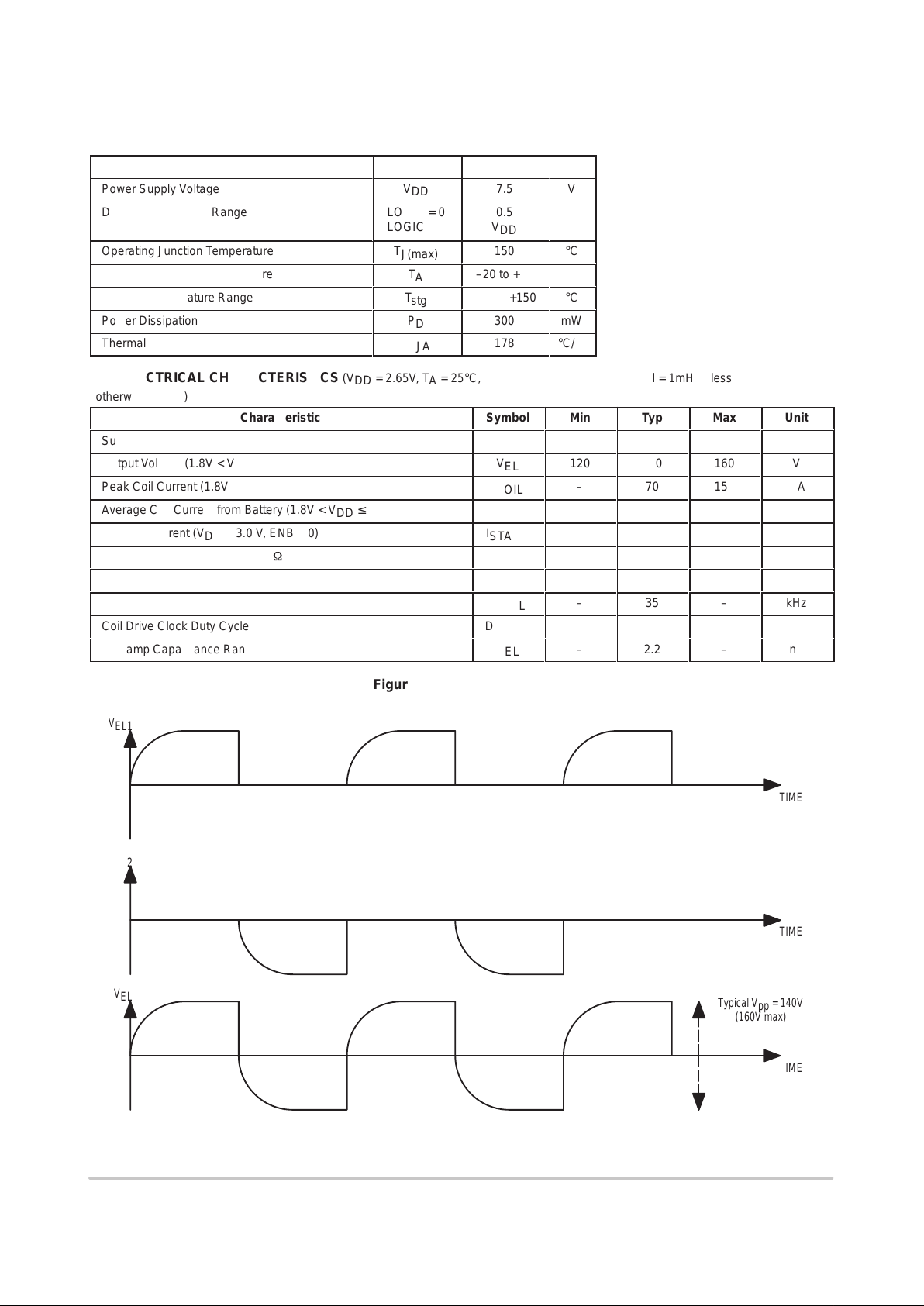
V
EL1
TIME
V
EL2
V
EL
TIME
TIME
Typical Vpp = 140V
(160V max)
Figure 2. Output Waveform
MC33441
http://onsemi.com
4
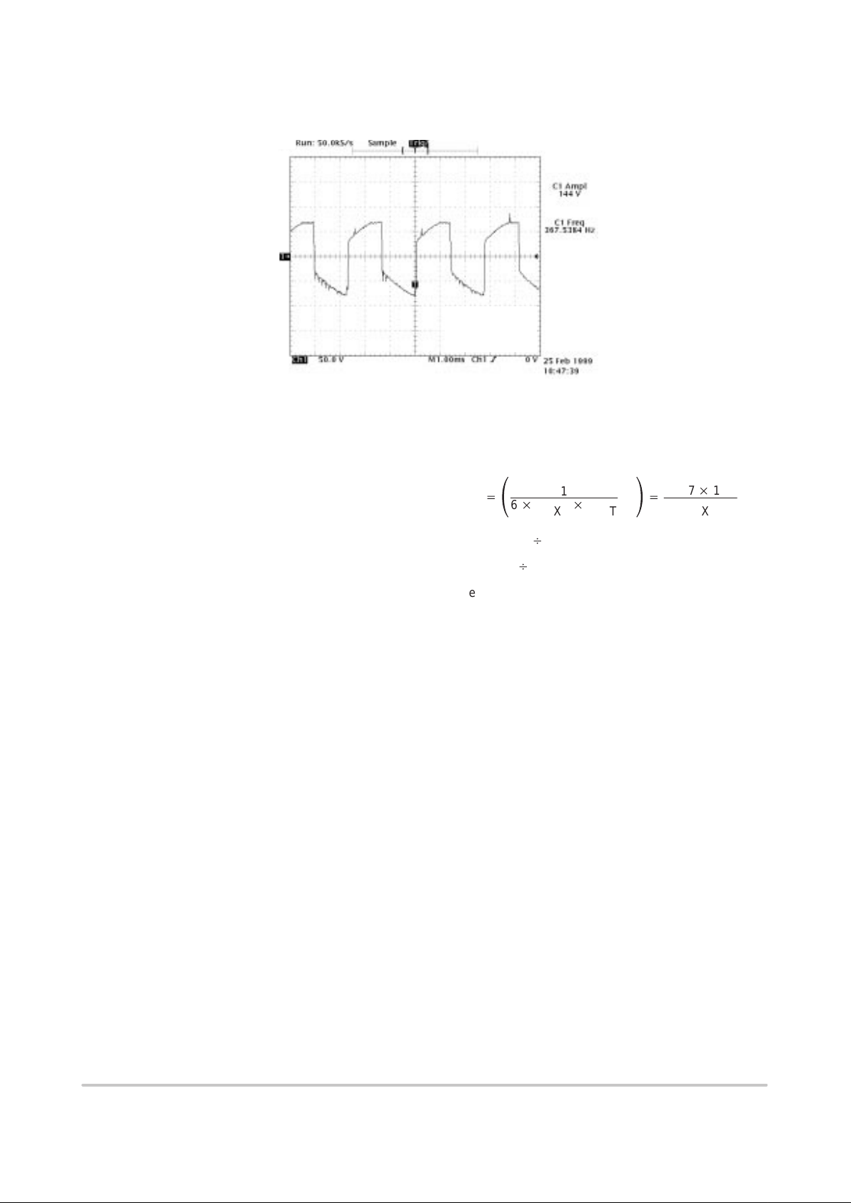
Figure 3. Output Waveform vs. Time
VDD = 2.65V
Lamp Freq. = 365Hz
EL Lamp = 2.2nF
X = 1ms/div, Y = 50V/div
OPERA TING DESCRIPTION
General
The MC33441 is a DC–AC inverter integrated circuit for
driving EL lamps. It can boost the supply voltage to the level
required by EL lamps and also provide high voltage AC lamp
excitation. It consists of an oscillator, a frequency divider, a coil
driving circuit and a switched H–bridge network. The input
supply voltage range is from 1.8V to 3.5V and is capable to
supply a typical 140Vpp AC output voltage. The standby
current of the device is typically 10nA which is ideal for low
power portable products. Externally, one inductor and one
resistor are needed to generate the desirable voltage charge and
to fine tune the oscillator’s frequency. This device is offered in
8–Pin TSSOP packages. The operating temperature is –20°C to
70°C.
Oscillator and Frequency Divider
Two circuits are put together to form the oscillator. They are
Vref and Ibias. The functionality of Vref block is to generate a
zero temperature coefficient (TC) voltage reference which is
about 1.27V. This 1.27V will then be used in Ibias circuit to
provide current biasing to all of the internal circuits with the
value equal to Vref divided by an internal resistor. Besides of
that, an external resistor is also connected to this circuit block for
setting the oscillator’s frequency. The temperature coefficient is
dominated by the value of that resistor. Therefore, if a low TC
resistor is used, the oscillator frequency’s TC can be kept low.
The current mirrors with the induced current equal to the Vref
divided by an external resistor are used to charge and discharge
an internal capacitor to provide a 50% duty cycle clock signal.
This original clock pulse will then be fed into the frequency
divider which will generate two additional clock signals with
different frequency and duty cycle to the coil–driver and the
H–bridge circuits. The oscillator frequency is governed by the
following equation:
F
OSC
+
ǒ
1
6 R
EXT
C
INT
HzǓ+
1.667 10
10
R
EXT
Hz
F
COIL
= F
OSC
B 4
FEL = F
OSC
B 384
where C
INT
is about 10pF.
Coil Driver
The coil driver is basically a simplified boost converter. It
takes a higher frequency clock signal from the frequency divider
to turn on/off the main switch alternatively. When the main
switch is on, current will flow through the coil to ground. Once
the switch is being turned off, the energy stored in the coil will
be released to the external capacitor (EL lamp) through an
internal diode. According to the frequency of the clock signals
between the coil driver and the H–bridge, the external capacitor
(EL lamp) will be charging to the desirable level.
Current limit circuit (typical 70mA & max. 150mA) is
implemented in this device. Since the current through the coil
will increase corresponding to the input voltage, if the input
voltage is high and the inductance of the coil is small, the coil
can be saturated. The current limit feature is used to avoid this
happen. The main switch is parallel to a much smaller switch
which has their collector and their base connected together.
However, the emitter of the smaller switch is tied to a sensing
resistor while the emitter of the main switch is connected to
ground. The coil current will split into two according to the
sizing ratio between the main and the smaller switch. The
current through the smaller switch will also flow through the
sensing resistor and generates a voltage. If the voltage across this
sensing resistor is above the pre–set value, then both switches
 Loading...