

MOTOROLA MC33375ST-3.3T3, MC33375D-5.0R2, MC33375ST-1.8T3, MC33375ST-2.5T3, MC33375D-3.3R2 Datasheet
...
MC33375
Advance Information
Low Dropout 300 mA
V oltage Regulator
with ON/OFF Control
The MC33375 series are micropower low dropout voltage
regulators available in a wide variety of output voltages as well as
packages, SOT–223, and SOP–8 surface mount packages. These
devices feature a very low quiescent current and are capable of
supplying output currents up to 300 mA. Internal current and thermal
limiting protection are provided by the presence of a short circuit at the
output and an internal thermal shutdown circuit.
The MC33375 has a control pin that allows a logic level signal to
turn–off or turn–on the regulator output.
Due to the low input–to–output voltage differential and bias current
specifications, these devices are ideally suited for battery powered
computer, consumer, and industrial equipment where an extension of
useful battery life is desirable.
Features:
• Low Quiescent Current (0.3
• Low Input–to–Output Voltage Differential of 25 mV at I
and 260 mV at I
= 300 mA
O
• Extremely Tight Line and Load Regulation
• Stable with Output Capacitance of only 0.33
Voltage
• Internal Current and Thermal Limiting
• Logic Level ON/OFF Control
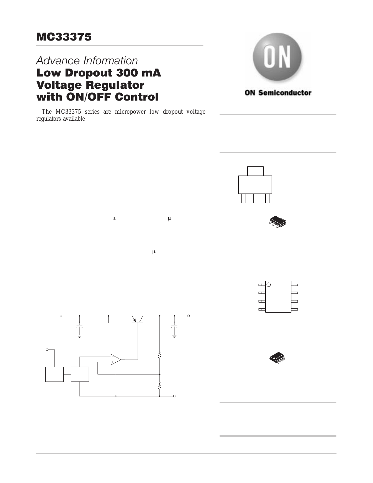
Simplified Block Diagram
V
in
m
A in OFF mode; 125 mA in ON mode)
= 10 mA,
O
m
F for 2.5 V Output
V
out
http://onsemi.com
LOW DROPOUT
MICROPOWER VOLTAGE
REGULATOR
Gnd
4
AYW
375xx
123
V
ON/OFF
in
1
Input
2
Gnd
3
Gnd
ON/OFF
4
A = Manufacturing Code
YW = Date
xx = Version
V
out
4
1
3
PLASTIC
ST SUFFIX
CASE 318E
ALYW
375xx
8
Output
7
Gnd
6
Gnd
5
N/C
Thermal &
Anti–sat
On/Off
On/Off
Block
This document contains information on a new product. Specifications and information
herein are subject to change without notice.
Semiconductor Components Industries, LLC, 2000
March, 2000 – Rev . 4
1.23 V
V. Ref.
Protection
Rint
54 K
Gnd
This device contains 41 active transistors
1 Publication Order Number:
Pins 4 and 5 Not Connected
AL = Manufacturing Code
YW = Date
xx = Version
8
1
PLASTIC
D SUFFIX
CASE 751
ORDERING INFORMATION
See detailed ordering and shipping information in the
package dimensions section on page 10 of this data sheet.
MC33375/D
MC33375
ELECTRICAL CHARACTERISTICS (C
Characteristic
Output Voltage IO = 0 mA to 250 mA
1.8 V Suffix T
2.5 V Suffix
3.0 V Suffix
3.3 V Suffix
5.0 V Suffix
1.8 V Suffix V
2.5 V Suffix 2% Tolerance from T
3.0 V Suffix
3.3 V Suffix
5.0 V Suffix
Line Regulation Vin = [VO + 1] V to 12 V, IO = 250 mA,
Load Regulation Vin = [VO + 1] V, IO = 0 mA to 250 mA,
Dropout Voltage
= 10 mA TJ = –40°C to +125°C
I
O
I
= 100 mA
O
= 250 mA
I
O
= 300 mA
I
O
Ripple Rejection (120 Hz) V
Output Noise Voltage
C
= 1 mFI
L
C
= 200 mF
L
= 25°C, Vin = [VO + 1] V
A
= [VO + 1] V, 0 < IO < 100 mA
in
All Suffixes T
All Suffixes T
= 50 mA (10 Hz to 100 kHz)
O
= 25°C
A
= 25°C
A
in(peak–peak)
= 1.0µF, TA = 25°C, for min/max values TJ = –40°C to +125°C, Note 1)
L
Symbol Min Typ Max Unit
V
= –40 to +125°C
J
O
Reg
Reg
load
Vin – V
line
1.782
2.475
2.970
3.267
4.950
1.764
2.450
2.940
3.234
4.900
1.80
2.50
3.00
3.30
5.00
—
—
—
—
—
1.818
2.525
3.030
3.333
5.05
1.836
2.550
3.060
3.366
5.100
– 2.0 10 mV
– 5.0 25 mV
O
—
—
—
—
25
115
220
260
100
200
400
500
= [VO + 1.5] V to [VO + 5.5] V — 65 75 — dB
V
n
—
—
160
46
—
—
CURRENT PARAMETERS
Quiescent Current
On Mode V
= [VO + 1] V, IO = 0 mA
in
Off Mode
On Mode SAT V
= [VO – 0.5] V, IO = 0 mA, Note 2
in
Current Limit Vin = [VO + 1] V, VO shorted I
I
Q
LIMIT
—
—
—
125
0.3
1100
200
4.0
1500
— 450 — mA
ON/OFF INPUTS
On/Off Input Voltage
Logic “1” (Regulator On) V
Logic “0” (Regulator Off) V
Logic “0” (Regulator Off) V
= VO ± 2%
out
< 0.03V
out
< 0.05V (1.8 V Option)
out
V
CTRL
2.4
—
—
—
—
—
—
0.5
0.3
THERMAL SHUTDOWN
Thermal Shutdown — — 150 — °C
NOTE: 1. Low duty pulse techniques are used during test to maintain junction temperature as close to ambient as possible.
NOTE: 2. Quiescent Current is measured where the PNP pass transistor is in saturation. V
= [VO – 0.5] V guarantees this condition.
in
Vdc
mV
m
Vrms
m
A
V
http://onsemi.com
2
MC33375
DEFINITIONS
Load Regulation – The change in output voltage for a
change in load current at constant chip temperature.
Dropout V oltage – The input/output differential at which
the regulator output no longer maintains regulation against
further reductions in input voltage. Measured when the
output drops 100 mV below its nominal value (which is
measured at 1.0 V differential), dropout voltage is affected
by junction temperature, load current and minimum input
supply requirements.
Output Noise Voltage – The RMS AC voltage at the
output with a constant load and no input ripple, measured
over a specified frequency range.
Maximum Power Dissipation – The maximum total
dissipation for which the regulator will operate within
specifications.
Quiescent Current – Current which is used to operate the
regulator chip and is not delivered to the load.
Line Regulation – The change in output voltage for a
change in the input voltage. The measurement is made under
conditions of low dissipation or by using pulse techniques
such that the average chip temperature is not significantly
affected.
Maximum Package Power Dissipation – The maximum
package power dissipation is the power dissipation level at
which the junction temperature reaches its maximum value
i.e. 150°C. The junction temperature is rising while the
difference between the input power (V
output power (V
out
X I
out
) is increasing.
X ICC) and the
CC
Depending on ambient temperature, it is possible to
calculate the maximum power dissipation and so the
maximum current as following:
TJ–T
Pd
+
A
R
q
JA
The maximum operating junction temperature TJ is
specified at 150°C, if TA = 25°C, then PD can be found. By
neglecting the quiescent current, the maximum power
dissipation can be expressed as:
P
I
out
+
D
VCC–V
out
The thermal resistance of the whole circuit can be
evaluated by deliberately activating the thermal shutdown
of the circuit (by increasing the output current or raising the
input voltage for example).
Then you can calculate the power dissipation by
subtracting the output power from the input power. All
variables are then well known: power dissipation, thermal
shutdown temperature (150°C for MC33375) and ambient
temperature.
TJ–T
R
+
q
JA
A
P
D
http://onsemi.com
3
MC33375
Figure 1. Line Transient Response Figure 2. Line Transient Response
7
TA = 25° C
6
= 0.47 mF
C
IL = 10 mA
V
5
L
= 3.3 V
out
V
in
4
3
, INPUT VOLTAGE (V)
2
in
V
V
out
1
0
0
20 40 60 80 100 120 140 160 180 200
TIME (mS)
Figure 3. Load Transient Response
300
–100
–200
–300
–400
LOAD CURRENT (mA)
–500
–600
–700
200
100
0
CL = 1.0 mF
V
= 3.3 V
out
TA = 25° C
Vin = 4.3 V
0
50 100 150 200 250 400
LOAD CURRENT
V
CHANGE
out
TIME (mS)
300 350
200
OUTPUT VOLTAGE CHANGE (mV)
150
100
50
0
–50
–100
1.0
0.8
OUTPUT VOLTAGE CHANGE (V)
0.6
0.4
0.2
0
–0.2
–0.4
–0.6
–0.8
–1.0
7
TA = 25° C
6
C
= 33 mF
IL = 10 mA
V
5
L
out
= 3.3 V
V
in
4
3
2
, INPUT VOLTAGE (V)
in
V
1
V
out
0
0
50 100 150 200
TIME (mS)
Figure 4. Load Transient Response
350
250
150
50
–50
–150
–250
–350
–450
LOAD CURRENT (mA)
–550
–650
–750
0 250 300
LOAD CURRENT
V
CHANGE
out
50 100 150
TIME (mS)
200
CL = 33.0mF
V
out
T
= 25° C
A
Vin = 4.3 V
= 3.3 V
70
OUTPUT VOLTAGE CHANGE (mV)
60
50
40
30
20
10
0
–10
–20
0.14
OUTPUT VOLTAGE CHANGE (V)
0.09
0.04
–0.01
–0.06
–0.11
–0.16
Figure 5. Output Voltage versus Input Voltage
3.5
OUTPUT VOLTAGE (V)
3.0
2.5
2.0
1.5
1.0
0.5
0
0.5
0
1.0
IL = 1 mA
1.5 2.0
2.5
INPUT VOLTAGE (V)
IL = 250 mA
3.0 3.5 4.0
Figure 6. Dropout Voltage versus Output Current
300
250
200
150
100
DROPOUT VOLTAGE (mV)
50
0
4.5
5.0
1
http://onsemi.com
4
10 100 1000
IO, OUTPUT CURRENT (mA)
 Loading...