

MOTOROLA MC33363BP, MC33363BDW, MC33363BDWR2 Datasheet
Order this document by MC33363B/D
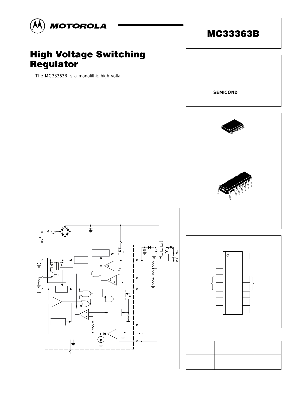
The MC33363B is a monolithic high voltage switching regulator that is
specifically designed to operate from a rectified 240 Vac line source. This
integrated circuit features an on–chip 700 V/1.0 A SenseFET power switch,
450 V active off–line startup FET, duty cycle controlled oscillator, current
limiting comparator with a programmable threshold and leading edge
blanking, latching pulse width modulator for double pulse suppression, high
gain error amplifier, and a trimmed internal bandgap reference. Protective
features include cycle–by–cycle current limiting, input undervoltage lockout
with hysteresis, overvoltage protection, and thermal shutdown. This device
is available in a 16–lead dual–in–line and wide body surface mount
packages.
• On–Chip 700 V, 1.0 A SenseFET Power Switch
• Rectified 240 V ac Line Source Operation
• On–Chip 450 V Active Off–Line Startup FET
• Latching PWM for Double Pulse Suppression
• Cycle–By–Cycle Current Limiting
• Input Undervoltage Lockout with Hysteresis
• Over–Voltage Protection
• Trimmed Internal Bandgap Reference
• Internal Thermal Shutdown
Simplified Application
HIGH VOLTAGE
OFF–LINE
SWITCHING REGULATOR
SEMICONDUCTOR
TECHNICAL DATA
16
1
DW SUFFIX
PLASTIC PACKAGE
CASE 751N
(SOP–16L)
16
1
P SUFFIX
PLASTIC PACKAGE
CASE 648E
(DIP–16)
AC Input
Startup Input
Regulator
Output
8
6
R
T
C
7
T
Mirror
Reg
Osc
PWM
Thermal
Gnd 4, 5, 12, 13
Startup
PWM Latch
S
Q
R
I
pk
Driver
EA
MOTOROLA ANALOG IC DEVICE DATA
LEB
1
UVLO
OVP
V
CC
3
Overvoltage
Protection
Input
11
16
Power Switch
Drain
Compensation
9
10
Voltage
Feedback
Input
DC Output
PIN CONNECTIONS
Startup Input
V
CC
Gnd
R
T
C
T
Regulator Output
116
3
4
5
6
7
8
(Top View)
Power Switch
Drain
13
Gnd
12
Overvoltage
11
Protection Input
Voltage Feedback
10
Input
Compensation
9
ORDERING INFORMATION
Operating
Device
MC33363BDW
MC33363BP DIP–16
Motorola, Inc. 1999 Rev 1
Temperature Range
TJ = –25° to +125°C
Package
SOP–16L
1
MAXIMUM RATINGS
Á
Á
Á
Á
Á
Á
Á
Á
Á
Á
Á
Á
Á
Á
Á
Á
Á
Á
Á
Á
Á
Á
Á
Á
Á
Á
Á
Á
Á
Á
Á
Á
Á
Á
Á
Á
ÁÁÁ
ÁÁÁ
ÁÁÁ
ÁÁÁ
Á
Á
Á
Á
Á
Á
Á
Á
Á
Á
Á
Á
Á
Á
Á
Á
Á
Á
Á
Á
ÁÁÁ
Á
Á
Á
Á
ÁÁÁ
ÁÁÁ
ÁÁÁ
ÁÁÁ
ÁÁÁ
ÁÁÁ
Á
Á
Á
Á
Á
ÁÁÁ
Á
Rating Symbol Value Unit
Power Switch (Pin 16)
Drain Voltage
ББББББББББББ
Drain Current
Startup Input Voltage (Pin 1, Note 1)
ББББББББББББ
Pin 3 = Gnd
Pin 3 ≤ 1000 µF to ground
ББББББББББББ
Power Supply Voltage (Pin 3)
Input Voltage Range
Voltage Feedback Input (Pin 10)
ББББББББББББ
Compensation (Pin 9)
Overvoltage Protection Input (Pin 11)
ББББББББББББ
RT (Pin 6)
ББББББББББББ
CT (Pin 7)
Thermal Characteristics
P Suffix, Dual–In–Line Case 648E
ББББББББББББ
Thermal Resistance, Junction–to–Air
Thermal Resistance, Junction–to–Case
ББББББББББББ
DW Suffix, Surface Mount Case 751G
Thermal Resistance, Junction–to–Air
Thermal Resistance, Junction–to–Case
ББББББББББББ
Operating Junction Temperature
Storage Temperature
NOTE: ESD data available upon request.
MC33363B
V
DS
ÁÁ
I
DS
V
in
ÁÁ
ÁÁ
V
CC
V
IR
ÁÁ
ÁÁ
ÁÁ
ÁÁ
R
θJA
R
ÁÁ
θJC
R
θJA
R
ÁÁ
θJC
T
J
T
stg
700
ÁÁÁ
1.0
ÁÁÁ
400
500
ÁÁÁ
40
–1.0 to V
ÁÁÁ
ÁÁÁ
ÁÁÁ
ÁÁÁ
ÁÁÁ
reg
80
15
95
15
ÁÁÁ
–25 to +150
–55 to +150
V
Á
A
V
Á
Á
V
V
Á
Á
Á
°C/W
Á
Á
Á
°C
°C
ELECTRICAL CHARACTERISTICS (V
= 20 V, RT = 10 k, CT = 390 pF, C
CC
= 1.0 µF, for typical values TJ = 25°C,
Pin 8
for min/max values TJ is the operating junction temperature range that applies (Note 2), unless otherwise noted.)
Characteristic
Symbol Min Typ Max Unit
REGULAT OR (Pin 8)
Output Voltage (IO = 0 mA, TJ = 25°C)
Line Regulation (VCC = 20 V to 40 V)
Load Regulation (IO = 0 mA to 10 mA)
Total Output Variation over Line, Load, and Temperature
V
Reg
Reg
V
reg
load
reg
line
5.5
–
–
5.3
OSCILLAT OR (Pin 7)
Frequency
CT = 390 pF
БББББББББББББББББ
TJ = 25°C (VCC = 20 V)
TJ = T
БББББББББББББББББ
CT = 2.0 nF
БББББББББББББББББ
TJ = 25°C (VCC = 20 V)
TJ = T
БББББББББББББББББ
low
low
to T
to T
(VCC = 20 V to 40 V)
high
(VCC = 20 V to 40 V)
high
Frequency Change with Voltage (VCC = 20 V to 40 V)
f
OSC
ÁÁÁ
ÁÁÁ
ÁÁÁ
ÁÁÁ
∆f
/∆V
OSC
ÁÁ
260
255
ÁÁ
ÁÁ
60
59
ÁÁ
–
ERROR AMPLIFIER (Pins 9, 10)
Voltage Feedback Input Threshold
Line Regulation (VCC = 20 V to 40 V, TJ = 25°C)
Input Bias Current (VFB = 2.6 V, TJ = 0 – 125°C)
Open Loop Voltage Gain (TJ = 25°C)
Gain Bandwidth Product (f = 100 kHz, TJ = 25°C)
V
Reg
A
GBW
FB
line
I
IB
VOL
2.52
–
–
70
0.85
Output Voltage Swing
High State (I
БББББББББББББББББ
Low State (I
NOTES: 1. Maximum power dissipation limits must be observed.
2.Tested junction temperature range for the MC33363B:
2
= 100 µA, VFB < 2.0 V)
Source
= 100 µA, V
Sink
T
= –25°CT
low
> 3.0 V)
FB
high
= +125°C
V
OH
ÁÁÁ
V
OL
4.0
ÁÁ
–
MOTOROLA ANALOG IC DEVICE DATA
6.5
30
44
–
ÁÁ
285
–
ÁÁ
ÁÁ
67.5
–
ÁÁ
0.1
2.6
0.6
20
82
1.0
5.3
ÁÁ
0.2
7.5
500
200
8.0
ÁÁ
310
315
ÁÁ
ÁÁ
75
76
ÁÁ
2.0
2.68
5.0
500
94
1.15
–
ÁÁ
0.35
V
mV
mV
V
kHz
ÁÁ
ÁÁ
ÁÁ
ÁÁ
kHz
V
mV
nA
dB
MHz
V
ÁÁ
MC33363B
ÁÁÁ
ÁÁÁ
Á
Á
Á
Á
Á
ÁÁÁ
Á
Á
Á
Á
Á
Á
ÁÁÁ
Á
Á
Á
Á
Á
Á
ÁÁÁ
Á
ÁÁÁ
ÁÁÁ
ÁÁÁ
Á
Á
Á
Á
Á
ÁÁÁ
Á
ÁÁÁ
ÁÁÁ
ÁÁÁ
Á
Á
Á
Á
Á
ÁÁÁ
Á
ELECTRICAL CHARACTERISTICS (continued) (V
= 20 V, RT = 10 k, CT = 390 pF, C
CC
= 1.0 µF, for typical values TJ = 25°C,
Pin 8
for min/max values TJ is the operating junction temperature range that applies (Note 2), unless otherwise noted.)
Characteristic UnitMaxTypMinSymbol
OVERVOLTAGE DETECTION (Pin 11)
Input Threshold Voltage
Input Bias Current (Vin = 2.6 V, TJ = –25 – 125°C)
V
th
I
IB
2.47
–
100
PWM COMPARATOR (Pins 7, 9)
Duty Cycle
Maximum (VFB = 0 V)
БББББББББББББББББ
Minimum (VFB = 2.7 V)
DC
(max)
ÁÁÁ
DC
(min)
48
ÁÁ
–
ÁÁ
POWER SWITCH (Pin 16)
Drain–Source On–State Resistance (ID = 200 mA)
TJ = 25°C
БББББББББББББББББ
TJ = T
low
to T
high
Drain–Source Off–State Leakage Current
БББББББББББББББББ
VDS = 650 V
Rise Time
Fall Time
R
DS(on)
ÁÁÁ
I
D(off)
ÁÁÁ
t
r
t
f
–
ÁÁ
–
ÁÁ
–
–
–
ÁÁ
ÁÁ
OVERCURRENT COMPARATOR (Pin 16)
Current Limit Threshold (RT = 10 k)
I
lim
0.5
0.72
STARTUP CONTROL (Pin 1)
Peak Startup Current (Vin = 400 V) (Note 3)
VCC = 0 V
БББББББББББББББББ
VCC = (V
th(on)
– 0.2 V)
Off–State Leakage Current (Vin = 50 V, VCC = 20 V)
I
start
ÁÁÁ
I
D(off)
–
ÁÁ
–
–
ÁÁ
UNDERVOLTAGE LOCKOUT (Pin 3)
Startup Threshold (VCC Increasing)
Minimum Operating Voltage After Turn–On
V
th(on)
V
CC(min)
11
7.5
15.2
TOTAL DEVICE (Pin 3)
Power Supply Current
Startup (V
БББББББББББББББББ
Operating
NOTES: 3. The device can only guarantee to start up at high temperature below +115°C.
= 10 V, Pin 1 Open)
CC
I
CC
ÁÁÁ
–
ÁÁ
–
0.25
ÁÁ
2.6
50
15
0.2
50
50
2.0
2.0
40
9.5
3.2
2.73
500
V
nA
%
52
0
ÁÁ
ÁÁ
0
Ω
17
–
ÁÁ
39
ÁÁ
µA
ÁÁ
100
–
–
0.9
ÁÁ
ns
ns
A
mA
4.0
ÁÁ
11.5
4.0
200
18
ÁÁ
µA
V
V
mA
0.5
ÁÁ
5.0
ÁÁ
Figure 1. Oscillator Frequency
versus Timing Resistor
1.0 M
CT = 100 pF
500 k
CT = 200 pF
CT = 500 pF
200 k
CT = 1.0 nF
100 k
CT = 2.0 nF
50 k
, OSCILLAT OR FREQUENCY (Hz)
CT = 5.0 nF
20 k
OSC
f
CT = 10 nF
10 k
7.0
10 15 20 30 50
RT, TIMING RESISTOR (kΩ)
MOTOROLA ANALOG IC DEVICE DATA
VCC = 20 V
°
C
TA = 25
70
Figure 2. Power Switch Peak Drain Current
versus Timing Resistor
1.0
0.8
0.6
0.4
0.3
0.2
0.15
Inductor supply voltage and inductance value are
adjusted so that Ipk turn–off is achieved at 5.0
, POWER SWITCH PEAK DRAIN CURRENT (A)
0.1
PK
7.0 10 15 20 30 40 7050
I
RT, TIMING RESISTOR (kΩ)
µ
s.
VCC = 20 V
µ
CT = 1.0
TA = 25
F
°
C
3
0.8
0.5
Figure 3. Oscillator Charge/Discharge
Current versus Timing Resistor
VCC = 20 V
TA = 25
MC33363B
°
C
Figure 4. Maximum Output Duty Cycle
versus Timing Resistor Ratio
70
60
RD/RT Ratio
Discharge Resistor
Pin 6 to Gnd
VCC = 20 V
CT = 2.0 nF
°
C
TA = 25
0.3
, OSCILLAT OR
0.2
dscg
/I
0.15
chg
I
0.1
CHARGE/DISCHARGE CURRENT (mA)
0.08
7.0
100
80
60
40
20
, OPEN LOOP VOL TAGE GAIN (dB)
0
VOL
A
–20
10
50
40
, MAXIMUM OUTPUT DUTY CYCLE (%)
max
D
, OUTPUT SA TURATION VOLTAGE (V)
V
sat
30
–1.0
– 2.0
2.0
1.0
1.0
TIMING RESISTOR RA TIO
Figure 6. Error Amp Output Saturation
V oltage versus Load Current
0
Source Saturation
(Load to Ground)
Sink Saturation
(Load to V
0
0
IO, OUTPUT LOAD CURRENT (mA)
ref
)
10 15 20 30 70 2.0 3.0 5.0 7.0 10
RT, TIMING RESISTOR (kΩ)
50
Figure 5. Error Amp Open Loop Gain and
Phase versus Frequency
VCC = 20 V
VO = 1.0 to 4.0 V
Gain
Phase
100 1.0 k 10 k 100 k 1.0 M 10 M 0.2 0.4 0.6 0.8 1.0
f, FREQUENCY (Hz)
RL = 5.0 M
CL = 2.0 pF
TA = 25
Ω
°
C
0
30
60
90
120
, EXCESS PHASE (DEGREES)
θ
150
180
RC/RT Ratio
Charge Resistor
Pin 6 to V
V
ref
VCC = 20 V
TA = 25
Gnd
°
reg
C
1.80 V
1.75 V
1.70 V
4
Figure 7. Error Amplifier Small Signal
Transient Response
VCC = 20 V
AV = –1.0
CL = 10 pF
TA = 25
1.0 µs/DIV
Figure 8. Error Amplifier Large Signal
Transient Response
VCC = 20 V
AV = –1.0
°
C
20 mV/DIV
3.00 V
1.75 V
0.50 V
1.0 µs/DIV
CL = 10 pF
°
C
TA = 25
0.5 V/DIV
MOTOROLA ANALOG IC DEVICE DATA
 Loading...