

Page 1
查询MC33348供应商
Order this document by MC33347A/D
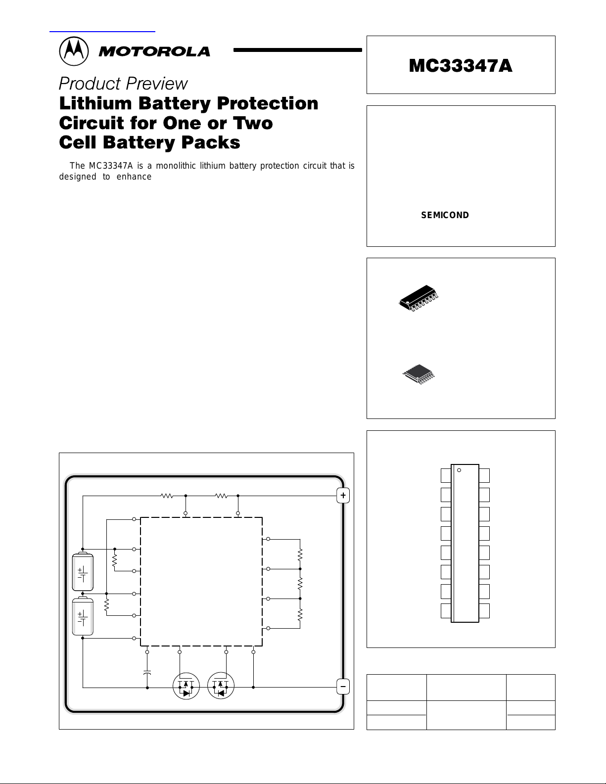
The MC33347A is a monolithic lithium battery protection circuit that is
designed to enhance the useful operating life of one or two cell
rechargeable battery packs. Cell protection features consist of
independently programmable charge and discharge limits for both voltage
and current, a delayed current shutdown, continuous cell voltage balancing
with the choice of on–chip or external balancing resistors, and a virtually
zero current sleepmode state when the cells are discharged.
Additional features include an on–chip charge pump for reduced
MOSFET losses while charging or discharging a low cell voltage battery
pack. This protection circuit requires a minimum number of external
components and is targeted for inclusion within the battery pack. This
MC33347A is available in standard and low profile 16 lead surface mount
packages.
• Programmable for One or Two Cell Applications
• Independently Programmable Charge and Discharge Limits for Both
Voltage and Current
• Charge and Discharge Current Limit Detection with Delayed Shutdown
• Continuous Cell Voltage Balancing
• On–Chip and External (optional) Balancing Resistors
• Virtually Zero Current Sleepmode State when Cells are Discharged
• Charge Pump for Reduced Losses with a Low Cell Voltage Battery Pack
• Minimum External Components for Inclusion within the Battery Pack
• Available in Low Profile Surface Mount Packages
LITHIUM BATTERY
PROTECTION CIRCUIT
FOR
ONE OR TWO CELL
SMART BATTERY PACKS
SEMICONDUCTOR
TECHNICAL DATA
D SUFFIX
16
1
16
1
PIN CONNECTIONS
PLASTIC PACKAGE
CASE 751B
(SO–16)
DTB SUFFIX
PLASTIC PACKAGE
CASE 948F
(TSSOP–16)
Typical Two Cell Smart Battery Pack
R
Lim(dschg)
13
4
Rb2
2
3
Rb1
1
16
15 14 12 11
CO
Discharge
MOSFET Q2
reserves the right to change or discontinue this product without notice.
MOTOROLA ANALOG IC DEVICE DATA
R
MC33347A
Lim(chg)
109
Charge
MOSFET Q1
Balance 1
Balance 2
Cell Voltage 1/V
Cell Voltage 1/VCC/
Discharge Current Limit/
6
R1
7
R2
8
R3
5
High Current Threshold
Cell Voltage Return
Cell Voltage Positive
Discharge Voltage
Threshold
Charge Voltage
Threshold
116
2
3
C
4
5
6
7
8
(Top View)
Ground
Charge Pump Output
15
Discharge
14
Gate Drive Output
Cell Program/
13
T est
Charge
12
Gate Drive Output
Charge
11
Gate Drive Common
Charge Current Limit/
10
Balance Disable
Current Sense
9
Common
ORDERING INFORMATION
Operating
Device
MC33347AD
MC33347ADTB
Motorola, Inc. 1999 Rev 0This document contains information on a product under development. Motorola
Temperature Range
TA = –40° to +85°C
Package
SO–16
TSSOP–16
1
Page 2
MC33347A
MAXIMUM RATINGS
Ratings Symbol Value Unit
Input Voltage (Measured with Respect to Ground, Pin 16)
Balance 1, 2 (Pins 1, 2) 10
Cell 1 (Pin 3) 7.5
Cell 2 (Pin 4) 10
Cell Voltage Divider (Pins 5, 6, 7 and 8) 10
Current Sense Common (Pin 9) 10
Charge Current Limit (Pin 10) 10
Charge Gate Drive Common (Pin 11) ±13
Charge Gate Drive Output (Pin 12) –14 to +12
Cell Program/Test (Pin 13) 10
Discharge Gate Drive Output (Pin 14) 10
Charge Pump Output (Pin 15) 10
External Cell Balancing Current (Pin 1, 2, Note 1)
Cell Voltage Divider Current
Source Current (Pin 4 to 6) or (Pin 3 to 6) 0.5
Sink Current (Pin 3 to 5) or (Pin 16 to 5) 0.5
Thermal Resistance, Junction–to–Air
DTB Suffix, TSSOP–16 Plastic Package, Case 948F 176
D Suffix, SO–16 Plastic Package, Case 751B 145
Operating Junction Temperature (Notes 1, 2 and 3)
Storage Temperature
NOTE: ESD data available upon request.
R
V
I
bal
I
div
θJA
T
T
IR
J
stg
1.0
–40 to +150
–55 to +150
V
A
mA
°C/W
°C
°C
ELECTRICAL CHARACTERISTICS (T
Characteristic
VOLTAGE SENSING
Charge or Discharge Voltage Inputs (Pin 7 or 8 to Pin 5)
Threshold Voltage V
TA = 25°C – 1.230 –
TA = T
Input Bias Current I
Input Hysteresis Source Current (Pin 8)
Cell Charge or Discharge Programmable Input Voltage Range (Pin 7 or 8)
Cell Selector Series Resistance
Cell Positive to Top of Divider (Pin 3 or 4 to Pin 6) R
Cell Negative to Bottom of Divider (Pin 3 or 16 to Pin 5) R
Cell Voltage Sampling Rate
V
Pin 9
V
Pin 9
Cell Program/ Test Input Threshold V oltage (Pin 13)
CELL VOLTAGE BALANCING
Cell Voltage Balancing Accuracy (Note 4)
Internal Balancing Resistance (Pin 3, 4)
Balancing MOSFET On Resistance (Pin 1, 2)
NOTES: 1. Maximum package power dissipation limits must be observed.
to T
low
high
< V
> V
2. Low duty cycle pulse techniques are used during test to maintain the junction temperature as close to ambient as possible.
3. Tested ambient temperature range for the MC33347A:
4. Cell balancing is active when the percent change in voltage exceeds the typical limit specified. This parameter is measured by holding one cell at a
fixed voltage while the other is varied so that balancing is activated. It is defined by:
+ 10mV – 1.0 –
Pin 4
+ 10mV – 0.004 –
Pin 4
T
= –25°CT
low
= 25°C unless otherwise noted.)
A
= +85°C
high
Variable Cell Voltage*Fixed Cell Voltage
ǒ
D%+
Fixed Cell Voltage
Symbol Min Typ Max Unit
th
– – –
IB
I
V
IR(pgm)
S+
t
(smpl)
V
V
bal
R
bal
R
DS(on)
H
S–
th
– 20 – nA
–
–
– 50 –
– 50 –
–
–
–
–
Ǔ
x 100
2.0
Vth to 7.5
V
Cell 1
1.0
100
1.0
/2.0
V
–
–
–
–
–
–
µA
V
Ω
s
V
∆%
Ω
Ω
2
MOTOROLA ANALOG IC DEVICE DATA
Page 3
MC33347A
Á
Á
Á
ELECTRICAL CHARACTERISTICS (continued) (T
= 25°C unless otherwise noted.)
A
Characteristic UnitMaxTypMinSymbol
CURRENT SENSING
Charge Current Limit (Pin 10 to Pin 9, TA = 25°C)
Threshold Voltage V
Input Bias Current I
Delay I
th(chg)
IB(chg)
dly(chg)
– 18 – mV
– 200 – nA
– 3.0 – ms
Discharge Current Limit (Pin 4 to Pin 9, TA = 25°C)
Threshold Voltage V
Input Bias Current I
Delay I
th(dschg)
IB(dschg)
dly(dschg)
– 70 – mV
– 200 – nA
– 3.0 – ms
CHARGE PUMP
Output Voltage (Pin 15, RL ≥ 1010 Ω)
V
O
–
9.2
TOTAL DEVICE
Average Cell Current (TA = 25°C, Battery Pack Unloaded and without
Current Limit Fault)
ББББББББББББББББББ
Operating with Soft Short (V
Pin 4
– V
> 10mV) – 19 –
Pin 9
I
CC
ÁÁ
ÁÁ
ÁÁÁÁÁÁÁÁ
Operating (VCC = 8.0 V) – 12.5 –
Sleepmode (VCC = 5.0 V) – 0.015 –
Minimum Operating Cell Voltage
V
CC
Programmed for Two Cell Operation
Cell 1 Voltage – 1.5 –
Cell 2 Voltage – 0 –
Programmed for One Cell Operation
Cell 1 Voltage – 1.5 –
NOTES: 1. Maximum package power dissipation limits must be observed.
2. Low duty cycle pulse techniques are used during test to maintain the junction temperature as close to ambient as possible.
3. Tested ambient temperature range for the MC33347A:
T
= –25°CT
low
4. Cell balancing is active when the percent change in voltage exceeds the typical limit specified. This parameter is measured by holding one cell at a
fixed voltage while the other is varied so that balancing is activated. It is defined by:
high
D%+
= +85°C
Variable Cell Voltage*Fixed Cell Voltage
ǒ
Fixed Cell Voltage
Ǔ
x 100
–
V
µA
V
MOTOROLA ANALOG IC DEVICE DATA
3
Page 4

MC33347A
Á
Á
Á
Á
Á
Á
БББББББББББББББББББББББ
Á
Á
Á
Á
Á
БББББББББББББББББББББББ
Á
Á
Á
Á
БББББББББББББББББББББББ
Á
Á
Á
Á
Á
Á
Á
Á
Á
Á
БББББББББББББББББББББББ
Á
Á
Á
БББББББББББББББББББББББ
Á
Á
Á
БББББББББББББББББББББББ
Á
Á
Á
Á
Á
Á
Á
Á
Á
Á
БББББББББББББББББББББББ
Á
Á
Á
Á
Á
Á
Á
Á
Á
БББББББББББББББББББББББ
Á
Á
Á
Á
Á
БББББББББББББББББББББББ
Á
Á
Á
Á
БББББББББББББББББББББББ
Á
Á
Á
Á
БББББББББББББББББББББББ
Á
Á
Á
Á
БББББББББББББББББББББББ
Á
Á
Á
Á
БББББББББББББББББББББББ
Á
Á
Á
Á
БББББББББББББББББББББББ
Á
БББББББББББББББББББББББ
БББББББББББББББББББББББ
PIN FUNCTION DESCRIPTION
Pin Pin Name Function Description
1
ÁÁ
ÁÁ
2
ÁÁ
3
ÁÁ
4
ÁÁ
ÁÁ
ÁÁ
ÁÁ5ÁÁ
6
ÁÁ
7
ÁÁ
ÁÁ
ÁÁ
8
ÁÁ
ÁÁ
9
ÁÁ
10
ÁÁ
11
ÁÁ
12
ÁÁ
13
ÁÁ
14
ÁÁ
15
16
BAL1
ÁÁ
ÁÁ
BAL2
ÁÁ
V1+
ÁÁ
V2+
ÁÁ
ÁÁ
ÁÁ
Ref_Gnd
CV+
ÁÁ
VL
ÁÁ
ÁÁ
ÁÁ
VH
ÁÁ
ÁÁ
OV Dchg
ÁÁ
OV Chg
ÁÁ
Pack–
ÁÁ
Cgate
ÁÁ
Prog
ÁÁ
Dgate
ÁÁ
Vpump
GND
Balance 1
ÁÁÁÁ
ÁÁÁÁ
Balance 2
ÁÁÁÁ
Cell Voltage 1/V
ÁÁÁÁ
Cell Voltage 2
ÁÁÁÁ
/VCC/Discharge
Current Limit/
ÁÁÁÁ
High Current
Threshold
ÁÁÁÁ
Cell Voltage
Return
ÁÁÁÁ
Cell Voltage
ÁÁÁÁ
Positive
Discharge
Voltage
ÁÁÁÁ
Threshold
ÁÁÁÁ
ÁÁÁÁ
Charge Voltage
Threshold
ÁÁÁÁ
ÁÁÁÁ
Current Sense
ÁÁÁÁ
Common
Charge Current
Limit/Cell
ÁÁÁÁ
Balance Disable
Charge Gate
ÁÁÁÁ
Drive Common
Charge Gate
Drive Output
ÁÁÁÁ
Cell Program
/Test
ÁÁÁÁ
Discharge Gate
Drive Output
ÁÁÁÁ
Charge Pump
Output
Ground
This is the drain connection to an internal MOSFET. An external resistor is placed from this pin
ББББББББББББББББББББББ
to the positive terminal of Cell 1 for increased cell balancing capability. This allows most of the
additional power to be dissipated off–chip.
ББББББББББББББББББББББ
This is the drain connection to an internal MOSFET. An external resistor is placed from this pin
to the positive terminal of Cell 2 for increased cell balancing capability. This allows most of the
ББББББББББББББББББББББ
additional power to be dissipated off–chip.
This is a multifunction pin that connects to a high impedance node of the Cell Selector where it
C
is used to monitor the positive terminal of Cell 1 and the negative terminal of Cell 2. This pin
ББББББББББББББББББББББ
also provides logic biasing and a discharge path for the internal balancing of Cell 1.
This is a multifunction pin that connects to a high impedance node of the Cell Selector where it
ББББББББББББББББББББББ
is used to monitor the positive terminal of Cell 2 and to provide positive supply voltage for the
protection IC. This pin is also used to monitor the voltage drop across the discharge current
ББББББББББББББББББББББ
limit resistor to detect a discharge current or a high current threshold to trigger fast sampling. It
also provides a discharge path for the internal balancing of Cell 2.
ББББББББББББББББББББББ
The bottom side of a three resistor divider string connects to this pin. The Cell Selector
internally switches this point to the negative terminal of the cell that is to be monitored.
ББББББББББББББББББББББ
The top side of a three resistor divider string connects to this pin. The Cell Selector internally
ББББББББББББББББББББББ
switches this point to the positive terminal of the cell that is to be monitored.
The upper tap of a three resistor divider string connects to this pin. The Cell Voltage Detector
compares the divided down cell voltage to an internal reference. If the comparator detects that
ББББББББББББББББББББББ
the cell voltage has fallen below the programmed level for three consecutive samples,
ББББББББББББББББББББББ
discharge switch Q2 is disabled, and the protection circuit enters into a low current sleepmode
state. This prevents further discharging of the battery pack.
ББББББББББББББББББББББ
The lower tap of a three resistor divider string connects to this pin. The Cell Voltage Detector
compares the divided down cell voltage to an internal reference. If the comparator detects that
ББББББББББББББББББББББ
the cell voltage has risen above the programmed level, charge switch Q1 is disabled,
preventing further charging of the battery pack. A 2.0 µA current source pull–up is internally
ББББББББББББББББББББББ
applied to this pin creating input hysteresis.
This pin is a common point that is used to monitor the voltage drop across the charge and
ББББББББББББББББББББББ
discharge current limit resistors.
This pin is used to monitor the voltage drop across the charge current limit resistor or if
connected to Pin 16, prevents cell balancing from occuring.
ББББББББББББББББББББББ
This pin provides a gate turn–off path for charge switch Q1. The charge switch source and the
ББББББББББББББББББББББ
battery pack negative terminal connect to this point.
This output connects to the gate of charge switch Q1 allowing it to enable or disable battery
pack charging.
ББББББББББББББББББББББ
This is a multifunction input that is used to program the number of cells and to facilitate circuit
testing. This input is connected to Pin 3 for two cell operation, and to Pin 16 for one cell
ББББББББББББББББББББББ
operation.
This output connects to the gate of discharge switch Q2 allowing it to enable or disable battery
pack discharging.
ББББББББББББББББББББББ
This is the charge pump output. A reservoir capacitor is connected from this pin to ground.
This is the protection IC ground and all voltage ratings are with respect to this pin.
4
MOTOROLA ANALOG IC DEVICE DATA
Page 5

MC33347A
Á
Á
Á
Á
Á
Á
Á
Á
Á
Á
Á
Á
Á
Á
Á
Á
Á
Á
Á
Á
Á
Á
Á
Á
Á
Á
Á
Á
Á
Á
Á
Á
Á
Á
Á
Á
Á
Á
Á
Á
Á
Á
Á
Á
Á
Á
Á
Á
Á
Á
Á
Á
Á
Á
Á
Á
Á
Á
Á
Á
Á
Á
Á
Á
Á
Á
Á
Á
Á
Á
Á
Á
Á
Á
Á
Á
Á
Á
Á
Á
Á
Á
Á
Á
Á
Á
Á
Á
Á
Á
Á
Á
Á
Á
Á
Á
Á
Á
Á
Á
Á
Á
Á
Á
Á
Á
Á
Á
Á
Á
Á
Á
Á
Á
Á
Á
Á
Á
Á
Á
Á
Á
Á
Á
Á
Á
Á
Á
Á
Á
Á
Á
Á
Á
Á
Á
Á
Á
Á
Á
Á
Á
Á
Á
Á
Á
Á
Á
Á
Á
Á
Á
Á
PROTECTION CIRCUIT OPERATING MODE TABLE
БББББББ
Input Conditions
БББББББ
CELL CHARGING/DISCHARGING
БББББББББББББББББББББ
Storage or Nominal Operation:
БББББББ
БББББББ
Cell Status
No current or voltage faults
CELL CHARGING FAULT/RESET
Charge Current Limit Fault:
V
≥ (V
Pin 10
БББББББ
for 3.0 ms
БББББББ
Pin 9
+ 18 mV)
Charge Current Limit Reset:
V
Pin 16
– V
БББББББ
БББББББ
БББББББ
Pin 11
< 2.0 V
Charge Voltage Limit Fault:
V
≥ 1.23 V for 1.0 s
Pin 8
БББББББ
БББББББ
БББББББ
Charge Voltage Limit Reset:
V
< 1.23 V for 1.0 s
Pin 8
БББББББ
БББББББ
CELL DISCHARGING FAULT/RESET
Discharge Current Limit Fault:
V
≤ (V
Pin 4
БББББББ
for 3.0 ms
БББББББ
Discharge Current Limit Reset:
БББББББ
V
– V
Pin 11
БББББББ
БББББББ
Pin 9
Pin 16
– 50 mV)
< 2.0 V
Discharge Voltage Limit Fault:
V
≤ 1.23 V for three
Pin 7
БББББББ
consecutive 1.0 s samples
БББББББ
Discharge Voltage Limit Reset:
V
> (V
Pin 16
БББББББ
БББББББ
Pin 11
+ 0.6 V)
FAULTY CELL (ONE CELL OVERVOLTAGE, ONE CELL UNDERVOLTAGE)
Simultaneous Charge and
Discharge Voltage Limit Faults:
БББББББ
V
≥ 1.23 V for 1 cell and
Pin 8
V
≤ 1.23 V for three
Pin 7
БББББББ
consecutive 1.0 s samples
БББББББ
БББББББ
NOTE: Cell balancing is not active when programmed for one cell operation.
БББББББББББББ
БББББББББББББ
Both Charge MOSFET Q1 and Discharge MOSFET
БББББББББББББ
Q2 are on. The battery pack is available for charging
or discharging.
БББББББББББББ
Circuit Operation
Battery Pack Status
Charge MOSFET Q1 is latched off and the cells are
disconnected from the charging source. Q1 will
БББББББББББББ
remain in the off state as long as V
V
by ≈ 2.0 V. The battery pack is available for
Pin 11
БББББББББББББ
discharging.
Pin 16
exceeds
The Sense Enable circuit will reset and turn on charge
MOSFET Q1 when V
БББББББББББББ
by ≈2.0 V. This can be accomplished by either
БББББББББББББ
disconnecting the charger from the battery pack, or by
connecting a load to the battery pack.
БББББББББББББ
no longer exceeds V
Pin 16
Pin 11
Charge MOSFET Q1 is latched off and the cells are
disconnected from the charging source. An internal
БББББББББББББ
current source pull–up of 2.0 µA is applied to Pin 8
creating an input hysteresis voltage of VH with divider
БББББББББББББ
resistors R1 and R2. The battery pack is available for
БББББББББББББ
discharging.
Charge MOSFET Q1 will turn on when the voltage
across each cell falls sufficiently to overcome the
БББББББББББББ
input hysteresis voltage. This can be accomplished by
applying a load to the battery pack.
БББББББББББББ
Discharge MOSFET Q2 is latched off and the cells
are disconnected from the load. Q2 will remain in the
БББББББББББББ
off state as long as V
The battery pack is available for charging.
БББББББББББББ
The Sense Enable circuit will reset and turn on
БББББББББББББ
discharge MOSFET Q2 when V
exceeds V
БББББББББББББ
by either disconnecting the load from the battery pack,
БББББББББББББ
or by connecting the battery pack to the charger.
by ≈ 2.0 V. This can be accomplished
Pin 16
Pin 11
exceeds V
Pin 11
by ≈2.0 V.
Pin 16
no longer
Discharge MOSFET Q2 is latched off, the cells are
disconnected from the load, and the protection circuit
БББББББББББББ
enters a low current sleepmode state. The battery
БББББББББББББ
pack is available for charging.
The Sense Enable circuit will reset and turn on
discharge MOSFET Q2 when V
БББББББББББББ
by 0.6 V . This can be accomplished by connecting the
battery pack to the charger.
БББББББББББББ
Pin 16
exceeds V
Pin 11
This condition can happen if there is a defective cell in
the battery pack such as one of the cells is shorted.
БББББББББББББ
The protection circuit will remain in the sleepmode
state until the battery pack is connected to a charger.
БББББББББББББ
If Cell 2 is faulty and a charger is connected, the
БББББББББББББ
protection circuit will cycle in and out of sleepmode. If
Cell 1 is faulty (<1.5 V), the protection circuit logic will
БББББББББББББ
not function and the battery pack cannot be charged.
MOSFET Switches
Q1
On
On
On
On
On
ÁÁ
DischargeQ2Charge
ÁÁ
ÁÁ
On
ÁÁ
ÁÁ
On
ÁÁ
ÁÁ
On
ÁÁ
ÁÁ
ÁÁ
On
ÁÁ
ÁÁ
ÁÁ
On
ÁÁ
ÁÁ
On to Off
ÁÁ
ÁÁ
Off to On
ÁÁ
ÁÁ
ÁÁ
On to Off
ÁÁ
ÁÁ
Off to On
ÁÁ
ÁÁ
Cycles
Cell 1
ÁÁ
Good
ÁÁ
Disabled
ÁÁ
Cell 1
Faulty
ÁÁ
Charge
Á
Á
Á
On to Off
Á
Á
Off to On
Á
Á
Á
On to Off
Á
Á
Á
Off to On
Á
Á
Á
Á
Á
Á
Á
Á
Á
Á
Á
Cycles
Cell 1
Á
Good
Á
Disabled
Á
Cell 1
Faulty
Á
Outputs
ÁÁ
ÁÁ
ÁÁ
ÁÁ
ÁÁ
ÁÁ
ÁÁ
ÁÁ
ÁÁ
ÁÁ
ÁÁ
ÁÁ
ÁÁ
ÁÁ
ÁÁ
ÁÁ
ÁÁ
ÁÁ
Disabled
ÁÁ
ÁÁ
ÁÁ
ÁÁ
ÁÁ
ÁÁ
Disabled
ÁÁ
ÁÁ
Pump
Active
Active
Active
Active
Active
Active
Active
Active
Cycles
Cell 1
Good
Cell 1
Faulty
Function
Balancing
(See Note)
ÁÁ
ÁÁ
ÁÁ
ÁÁ
ÁÁ
ÁÁ
ÁÁ
ÁÁ
ÁÁ
ÁÁ
ÁÁ
ÁÁ
ÁÁ
ÁÁ
ÁÁ
ÁÁ
ÁÁ
ÁÁ
Disabled
ÁÁ
ÁÁ
ÁÁ
ÁÁ
Cycles
ÁÁ
ÁÁ
Disabled
ÁÁ
ÁÁ
Cell
Active
Active
Active
Active
Active
Active
Active
Active
Cell 1
Good
Cell 1
Faulty
MOTOROLA ANALOG IC DEVICE DATA
5
Page 6

MC33347A
Figure 1. Two Cell Smart Battery Pack
Cell 2
Cell 1
0.1
R
Lim(dschg)
MC33347A
Prog
13
V2+
4
R
B2
BAL2
V1+
R
B1
BAL1
GND
16
80
2
Cell
3
80
1
CkCk En
Oscillator
Selector
Cell Voltage
Balancing
Amplifier
Charge Pump
OV Dchg
Discharge
Overcurrent
Detector
Charge/Discharge
Gate Drivers
R
Lim(chg)
9
Charge Overcurrent
Balance Disable
Floating
Over/Under
Cell Voltage
Detector
&
Reference
Over/Under
Data Latch
&
Control Logic
10
OV Chg
Detector / Cell
Sense
Enable
CV+
6
VL
7
VH
8
Ref_Gnd
5
C
0.22
R1
R2
R3
I
Vpump CgateDgate 14 12 11 Pack–
15
C
O
Discharge
Switch
Q2
Components CI and Rg are mandatory. Refer to the Battery Pack Application text. The 100 nF capacitor that connects
across Cell 1 provides high frequency bypassing of the VC pin which powers the internal logic. This capacitor is desireable
in applications that have high load current spikes when used with high impedance type cells.
R
g
20 k
4.7 M
R
g
20 k
Charge
Switch
Q1
6
MOTOROLA ANALOG IC DEVICE DATA
Page 7

MC33347A
Figure 2. One Cell Smart Battery Pack
Cell 1
100
100
Prog
13
V2+
BAL2
V1+
BAL1
GND
16
R
Lim(dschg)
MC33347A
OV Dchg
Discharge
Overcurrent
Detector
4
80
R
Lim(chg)
9
Charge Overcurrent
Detector / Cell
Balance Disable
10
OV Chg
CV+
6
C
0.22
I
R1
2
Cell
3
80
Selector
Floating
Over/Under
Cell Voltage
Detector
&
Reference
1
VL
7
VH
8
Ref_Gnd
R2
R3
5
Cell Voltage
Balancing
Amplifier
Over/Under
Data Latch
&
Control Logic
Sense
CkCk En
Oscillator
Charge Pump
Charge/Discharge
Gate Drivers
Enable
Vpump CgateDgate 14 12 11
15
R
g
C
O
Discharge
20 k
R
20 k
Switch
Q2
Pack–
g
Charge
Switch
Q1
4.7 M
Components CI and Rg are mandatory. Refer to the Battery Pack Application text. In order to guarantee proper discharge
current limit operation when the battery pack output is shorted, power must be made available to the MC33347. An artifical
power source with a 10 ms time constant is required, and is provided by the 100 Ω resistor and 100 µF capacitor that
connects to the VCC and VC inputs. These components are only required in single cell battery pack applications.
Motorola reserves the right to make changes without further notice to any products herein. Motorola makes no warranty, representation or guarantee regarding
the suitability of its products for any particular purpose, nor does Motorola assume any liability arising out of the application or use of any product or circuit, and
specifically disclaims any and all liability, including without limitation consequential or incidental damages. “T ypical” parameters which may be provided in Motorola
data sheets and/or specifications can and do vary in different applications and actual performance may vary over time. All operating parameters, including “Typicals”
must be validated for each customer application by customer’s technical experts. Motorola does not convey any license under its patent rights nor the rights of
others. Motorola products are not designed, intended, or authorized for use as components in systems intended for surgical implant into the body, or other
applications intended to support or sustain life, or for any other application in which the failure of the Motorola product could create a situation where personal injury
or death may occur. Should Buyer purchase or use Motorola products for any such unintended or unauthorized application, Buyer shall indemnify and hold Motorola
and its officers, employees, subsidiaries, affiliates, and distributors harmless against all claims, costs, damages, and expenses, and reasonable attorney fees
arising out of, directly or indirectly, any claim of personal injury or death associated with such unintended or unauthorized use, even if such claim alleges that
Motorola was negligent regarding the design or manufacture of the part. Motorola and are registered trademarks of Motorola, Inc. Motorola, Inc. is an Equal
Opportunity/Affirmative Action Employer.
MOTOROLA ANALOG IC DEVICE DATA
7
Page 8
–T–
–T–
MC33347A
OUTLINE DIMENSIONS
PLASTIC PACKAGE
CASE 751B–05
–A–
16 9
–B–
18
G
K
SEATING
PLANE
D
16 PL
T
16X REFK
S
B
0.25 (0.010) A
M
0.10 (0.004) V
S
U0.15 (0.006) T
2X L/2
16
L
PIN 1
IDENT.
U0.15 (0.006) T
S
1
A
–V–
C
0.10 (0.004)
SEATING
PLANE
D
8 PLP
0.25 (0.010) B
C
M
S
DTB SUFFIX
PLASTIC PACKAGE
CASE 948F–01
(TSSOP–16)
M
S
U
T
9
B
–U–
8
H
G
D SUFFIX
(SO–16)
ISSUE J
M
R
ISSUE O
S
J
N
N
DETAIL E
S
X 45
_
J1
0.25 (0.010)
F
DETAIL E
F
J
K
K1
SECTION N–N
M
NOTES:
1. DIMENSIONING AND TOLERANCING PER ANSI
Y14.5M, 1982.
2. CONTROLLING DIMENSION: MILLIMETER.
3. DIMENSIONS A AND B DO NOT INCLUDE
MOLD PROTRUSION.
4. MAXIMUM MOLD PROTRUSION 0.15 (0.006)
PER SIDE.
5. DIMENSION D DOES NOT INCLUDE DAMBAR
PROTRUSION. ALLOWABLE DAMBAR
PROTRUSION SHALL BE 0.127 (0.005) TOTAL
IN EXCESS OF THE D DIMENSION AT
MAXIMUM MATERIAL CONDITION.
DIM MIN MAX MIN MAX
A 9.80 10.00 0.386 0.393
B 3.80 4.00 0.150 0.157
C 1.35 1.75 0.054 0.068
D 0.35 0.49 0.014 0.019
F 0.40 1.25 0.016 0.049
G 1.27 BSC 0.050 BSC
J 0.19 0.25 0.008 0.009
K 0.10 0.25 0.004 0.009
M 0 7 0 7
____
P 5.80 6.20 0.229 0.244
R 0.25 0.50 0.010 0.019
NOTES:
1 DIMENSIONING AND TOLERANCING PER ANSI
Y14.5M, 1982.
2 CONTROLLING DIMENSION: MILLIMETER.
3 DIMENSION A DOES NOT INCLUDE MOLD FLASH.
PROTRUSIONS OR GATE BURRS. MOLD FLASH
OR GATE BURRS SHALL NOT EXCEED 0.15
(0.006) PER SIDE.
4 DIMENSION B DOES NOT INCLUDE INTERLEAD
FLASH OR PROTRUSION. INTERLEAD FLASH OR
PROTRUSION SHALL NOT EXCEED
0.25 (0.010) PER SIDE.
5 DIMENSION K DOES NOT INCLUDE DAMBAR
PROTRUSION. ALLOWABLE DAMBAR
PROTRUSION SHALL BE 0.08 (0.003) TOTAL IN
EXCESS OF THE K DIMENSION AT MAXIMUM
MATERIAL CONDITION.
6 TERMINAL NUMBERS ARE SHOWN FOR
REFERENCE ONLY.
7 DIMENSION A AND B ARE TO BE DETERMINED
AT DATUM PLANE –W–.
DIM MIN MAX MIN MAX
A 4.90 5.10 0.193 0.200
B 4.30 4.50 0.169 0.177
C ––– 1.20 ––– 0.047
D 0.05 0.15 0.002 0.006
F 0.50 0.75 0.020 0.030
G 0.65 BSC 0.026 BSC
H 0.18 0.28 0.007 0.011
J 0.09 0.20 0.004 0.008
–W–
J1 0.09 0.16 0.004 0.006
K 0.19 0.30 0.007 0.012
K1 0.19 0.25 0.007 0.010
L 6.40 BSC 0.252 BSC
M 0 8 0 8
____
INCHESMILLIMETERS
INCHESMILLIMETERS
How to reach us:
Mfax is a trademark of Motorola, Inc.
USA/EUROPE / Locations Not Listed: Motorola Literature Distribution; JAPAN: Motorola Japan Ltd.; SPD, Strategic Planning Office, 141,
P.O. Box 5405, Denver, Colorado 80217. 1–303–675–2140 or 1–800–441–2447 4–32–1 Nishi–Gotanda, Shinagawa–ku, Tokyo, Japan. 81–3–5487–8488
Customer Focus Center: 1–800–521–6274
Mfax: RMFAX0@email.sps.mot.com – TOUCHTONE 1–602–244–6609 ASIA/PACIFIC: Motorola Semiconductors H.K. Ltd.; Silicon Harbour Centre,
Motorola Fax Back System – US & Canada ONLY 1–800–774–1848 2, Dai King Street, Tai Po Industrial Estate, Tai Po, N.T., Hong Kong.
– http://sps.motorola.com/mfax/ 852–26668334
HOME PAGE: http://motorola.com/sps/
8
◊
MOTOROLA ANALOG IC DEVICE DATA
MC33347A/D
 Loading...