

Page 1
MOTOROLA
SUNSTAR传感与控制 http://www.sensor-ic.com/ TEL:0755-83376549 FAX:0755-83376182 E-MAIL:szss20@163.com
SUNSTAR自动化 http://www.sensor-ic.com/ TEL: 0755-83376489 FAX:0755-83376182 E-MAIL:szss20@163.com
Semiconductor Technical Data
Advance Information
Order Number: MC33187/D
Rev. 4, 06/2001
MC33187
Long Duration Automotive Timer
This circuit is a Long Duration Automotive Timer primarily designed
as a deffoger timer, but as it is realised using a digital divider
techniques and it is suitable for a variety of long duration timing
functions. The circuit is available in an 8 pin surface plastic package.
• Operating Ambient Temperature from -40°C to 85°C
• Operating Voltage Range from 5V to 18V
• 400mA Output Current Capability
• Integrated Input Debounce Circuitry
• Few External Components
• Toggle Input for Timing Start and Stop
LONG DURATION AUTO-
MOTIVE TIMER
SEMICONDUCTOR
TECHNICAL DATA
D SUFFIX
PLASTIC PACKAGE
CASE 751
(SO-8)
PIN CONNECTIONS
1
RC
2
Gnd
3
Relay
4
Toggle
ORDERING INFORMATION
Device
MC33187D
Operating
Temperature Range
TS
8
N/C
7
N/C
6
Vcc3
5
Package
SO8-40°C to +85°C
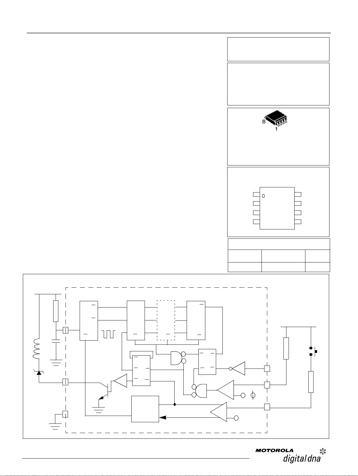
Block Diagram and Typical Application
Vbat
Q
C
Q
Q
C
C
12
Dz
Relay
R - C
1
3
Q
6.8 Hz
Q
C
Q
1
S
Q Q
D
Q
14
Q
R
Q
C
Q
C
S
C
S
J
Debounce Timer
Out
2
This document contains information on a new product. Specifications and information herein are
subject to change without notice.
© Motorola, Inc., 2001. All rights reserved.
Timing
In
R
Vbat
Q
S
Q
S1
13
TS
R
R
I
-
+
5
-
+
2.3V
8
5
VCC
4
Toggle
TM
Page 2
MC33187
SUNSTAR传感与控制 http://www.sensor-ic.com/ TEL:0755-83376549 FAX:0755-83376182 E-MAIL:szss20@163.com
SUNSTAR自动化 http://www.sensor-ic.com/ TEL: 0755-83376489 FAX:0755-83376182 E-MAIL:szss20@163.com
MAXIMUM RATINGS
Ratings Symbol Value Unit
ELECTRICAL RATINGS
Pin 5 voltage Vpin5 18 V
Pin 3 Voltage Vpin3 18 V
Pin 3 Current Ipin3 400 mA
THERMAL RATINGS
Storage Temperature Tstg -55 to +175 °C
Operating Junction Temperature Tj -40 to +150 °C
ELECTRICAL CHARACTERISTICS. Tamb from - 40°C to + 85°C, Vcc = 14V through 1KΩ, unless otherwise noted. Typical values reflect approximate
mean at 25°C, nominal VCC, at time of device characterization.
Parameters Symbol Min Typ Max Unit
RC PIN 1
Oscillator Frequency
fo 300 400 Hz
Vbat = 14V trough 1KΩ
Internal Counter Divider step VR1 4096
RELAY PIN 3
Output Leakage current @ Vpin3
IO1 100 uA
= 28V / Vbat =14V
Output Leakage current @ Vpin3
IO2 100 uA
= 22V / Vbat = 0V
Output Saturation Voltage @
VO1 1.35 V
250mA / Vbat = 14V
Output Saturation Voltage @
VO2 2.60 V
400mA
TOGGLE PIN 4
Toggle Input Clamp @ Vbat =
TCLP 6.0 9.0 V
14V / Vpin8 = 14V through 9.1KΩ
Toggle Threshold VTG-T 1.0 4.0 V
VCC3 PIN 5
Supply Current @ Vcc = 5V ICC 0.5 3.5 mA
VCC Zener Regulation @ Vbat =
VCC 6.0 8.0 V
14V through 1K
TS PIN 8
Time Select Current @ TS = 5V ITS 25 200 uA
MC33187 MOTOROLA 2
Page 3
MC33187
SUNSTAR传感与控制 http://www.sensor-ic.com/ TEL:0755-83376549 FAX:0755-83376182 E-MAIL:szss20@163.com
SUNSTAR自动化 http://www.sensor-ic.com/ TEL: 0755-83376489 FAX:0755-83376182 E-MAIL:szss20@163.com
DEVICE DESCRIPTION
Pin 1 : RC
Oscillator frequency control. Rt and Ct control the
frequency of the clock oscillator. The period of oscillation is
nominally given by t = RtCt with the overall time period given
by T = 4096 RtCt. However, the following formula is believed
to give a more accurate forecast of the overall time interval
provided by the circuit for values of Rt between 200K and 2M
and values of Ct between 1nF and 1uF.
Formula : T = 4.1 10e-3 (RT * (RT/150)*2.7) *CT.
Pin 2 : GND
Ground : Most negative supply terminal.
Pin 3 : RELAY
Relay output driver. Open collector drive from a Darlington
transistor rated. Icmax = 400mA and Vmax = 18V. The relay
driver output is on (low) during the time period.
APPLICATION
Pin 4 : TOGGLE
On/Off Control. A positive going voltage transition on this
input toggles the timer between the On and Off state. If the
timer is On and timing, it may be turned off by a positive going
signal on the toggle pin before the time delay has elapsed.
Pin 5 : VCC
Positive supply terminal. The timer requires a supply
voltage of 5 to 18V applied to Vcc through Rs. An internal 7V
zener limits the Vcc terminal voltage. Cs is included to provide
supply rail decoupling.
Recommended values of Rs and Cs on a standard 12V
vehicle system are Rs = 1KOhm and Cs = 100nF.
This is the standard operation of this circuit requiring the
minimum of extra components.
The ON/OFF switch is a non-latching push button (or
similar), illuminated by a lamp in parallel with the rear window
defogger. Rin protects the toggle input from supply line
transients with a nominal of Rin = 10KΩ. The relay is intended
to be a standard automotive relay (Rnom = 60Ω) with contacts
rated appropriately for the defogger controlled. Dz with a
nominal value of 16V +-5% is included to provide protection of
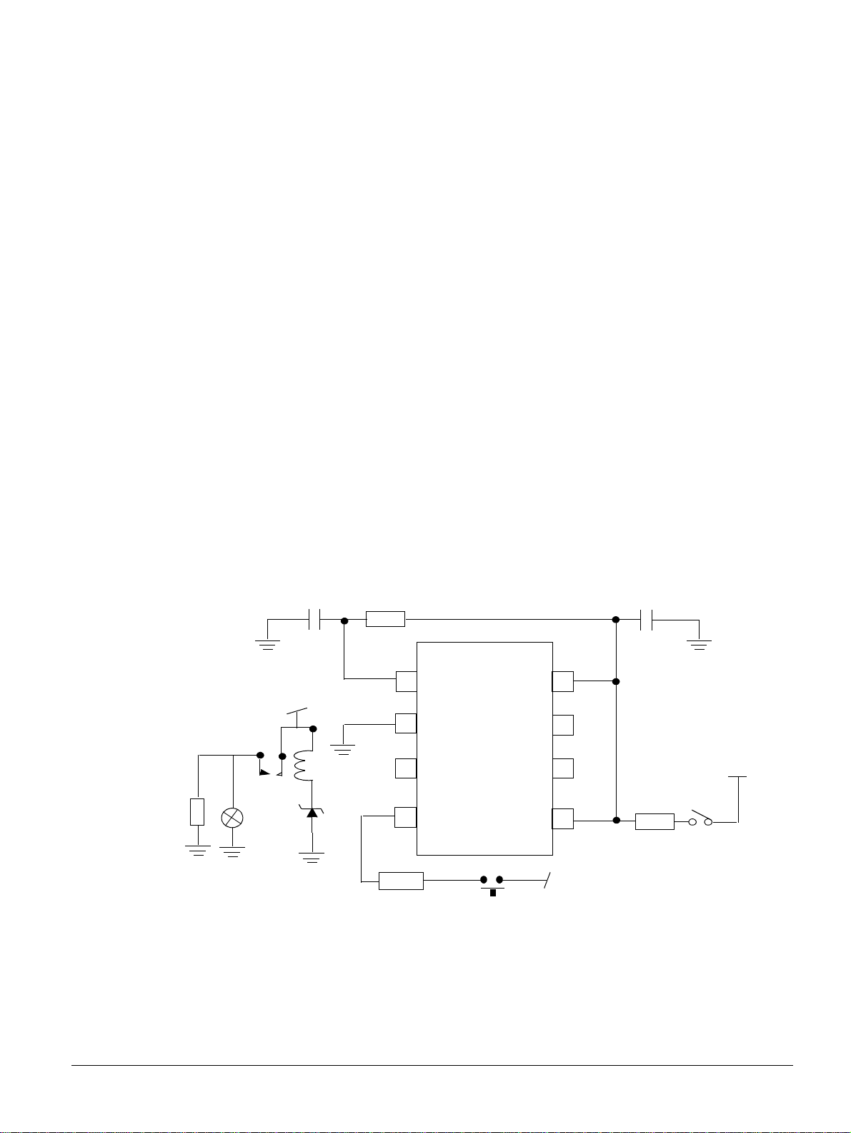
Figure 1. .Defogger Timer Operation
Ct
Batt
Rt
the relay drive output transistor against relay turn-off and
supply lines transients.
The type of zener used is dependent of the level of
protection required. An MZD16 will provide adequate
protection for all relay turn-off and low energy supply
transients, while a P6KE16A will provide full protection against
all known transients. If the relay output is to be connected in
any other way or to a non-standard relay, the maximum ratings
quoted under the General Description above should be noted.
Cs
RC
GND
Relay
TS
N / C
N / C
Batt
Rear
Defogger
Resistor
Dz
Rin
Toggle
S1
Vcc
Batt
MC33187 MOTOROLA 3
Rs
Page 4

MC33187
SUNSTAR传感与控制 http://www.sensor-ic.com/ TEL:0755-83376549 FAX:0755-83376182 E-MAIL:szss20@163.com
SUNSTAR自动化 http://www.sensor-ic.com/ TEL: 0755-83376489 FAX:0755-83376182 E-MAIL:szss20@163.com
The circuit shown demonstrates the use of the timer to
provide a delay in turning the courtesy light off after the
vehicle doors are closed. The components are the same as
the defogger timer and Rt, Ct, Rs and Cs are as described in
the general description above, while Dz and Rin are
described in the description of the defogger timer. S1 to Sn
represent the doors switches which can be basically the
same as for a conventional system, except that only the relay
coil current and not the full lamp current passes through
them.
The operation of the circuit is as follows :
While one of the door switches is closed, the courtesy
light is on with the relay current flowing through the switch.
Figure 2. Courtesy Light Timer Operation
As soon as the last switch is opened, the energy stored in
the relay coil causes the common connection of the switches
to rise to the voltage permitted by the clamp consisting of Dz
(approximately 16V).
This provides a toggle input via Rin, causing the relay
output of the integrated circuit to go low, thus keeping the
relay energised for the period preset, with the direct
connection to Rin ensuring that any switch bounce or noise
during this period cannot cause toggle input to be detected.
Retriggering at the end of the timing period is prevented by
the built in the debounce timer.
S1
Sn
Batt
Ct
Rin
Dz
Rt
RC
GND
Relay
Toggle
TS
N / C
N / C
Vcc
Cs
Batt
Rs
MC33187 MOTOROLA 4
Page 5

MC33187
SUNSTAR传感与控制 http://www.sensor-ic.com/ TEL:0755-83376549 FAX:0755-83376182 E-MAIL:szss20@163.com
SUNSTAR自动化 http://www.sensor-ic.com/ TEL: 0755-83376489 FAX:0755-83376182 E-MAIL:szss20@163.com
This circuit is designed to just use the toggle and relay
drive feature of the long duration timer.
The functions of components Rs, Cs, Rt, Ct, Rin and Dz
are as previously described. Although the circuit is not
intended to be allowed to time out, Rt and Ct need to be
included as it is necessary for the timer to run for the internal
debounce timer to be reset.
The control switch S1 needs to be a normally closed
momentary type.
While it is closed, D1 ensures that the oscillator does not
run, while R1 ensures that D1 is reverse biassed when the
switch is operated (open). C1 is included to provide a time
constant RinC1 to delay the detection of a toggle input.
Thus the operation of the circuit is as follows :
When S1 is operated, the oscillator is allowed to start ; the
toggle input is then recognised and the relay output changes
state assuming that the switch has been released, the
oscillator is stopped and the sequence above can be
repeated.
Figure 3. Relay Drive and Latch (No Timeout
If the switch is held operated for 9 seconds, with the
values recommended below, after it has been used to switch
the relay on the circuit will time out and the relay switch off.
No further action takes place until the circuit is reset by
releasing the button.
If the switch is held operated after it has been used to
switch the relay off, nothing happens until the circuit is reset
by releasing the button.
Recommended values :
Rs = 1KΩ
Cs = 100nF
Rt = 220KΩ
Ct = 10nF
Rin = 100KΩ
R1 = 1KΩ
C1 = 220nF
Dz = MZD16
D1 = 1N4148
Note that the time constant RtCt and RinC1 are related
(start up time and basic frequency of oscillator/switch to
toggle delay time) and need to stay in the ratio (1:10).
D1
Dz
Ct
Batt
C1
Rin
Rt
S1
RC
GND
Relay
Toggle
N / C
N / C
R1
Cs
TS
Batt
Rs
Vcc
MC33187 MOTOROLA 5
Page 6

MC33187 MOTOROLA 6
SUNSTAR传感与控制 http://www.sensor-ic.com/ TEL:0755-83376549 FAX:0755-83376182 E-MAIL:szss20@163.com
SUNSTAR自动化 http://www.sensor-ic.com/ TEL: 0755-83376489 FAX:0755-83376182 E-MAIL:szss20@163.com
Page 7

Motorola reserves the right to make changes without further notice to any products herein. Motorola makes no warranty, representation or guarantee regarding the suitability
SUNSTAR传感与控制 http://www.sensor-ic.com/ TEL:0755-83376549 FAX:0755-83376182 E-MAIL:szss20@163.com
SUNSTAR自动化 http://www.sensor-ic.com/ TEL: 0755-83376489 FAX:0755-83376182 E-MAIL:szss20@163.com
of its products for any particular purpose, nor does Motorola assume any liability arising out of the application or use of any product or circuit, and specifically disclaims any and all
liability, including without limitation consequential or incidental damages. “Ty pica l” parameters which may be provided in Motorola data sheets and/or specifications can and do
vary in different applications and actual performance may vary over time. All operating parameters, including “Typi cal ” must be validated for each customer application by
customer’s technical experts. Motorola does not convey any license under its patent rights nor the rights of others. Motorola products are not designed, intended, or authorized for
use as components in systems intended for surgical implant into the body, or other applications intended to support or sustain life, or for any application in which the failure of the
Motorola product could create a situation where personal injury or death may occur. Should Buyer purchase or use Motorola products for any such unintended or unauthorized
application, Buyer shall indemnify and hold Motorola and its officers, employees, subsidiaries, affiliates, and distributors harmless against all claims, costs, damages, and
expenses, and reasonable attorney fees arising out of, directly or indirectly, any claim of personal injury or death associated with such unintended or un authorized use, even if
such claim alleges that Motorola was negligent regarding the design or manufacture of the parts. Motorola and are registered trademarks of Motorola, Inc. Motorola, Inc. is
an Equal Employment Opportunity/Affirmative Action Employer.
How to reach us:
USA / EUROPE / Locations Not Listed: Motorola Literature Distribution; JAPAN: Motorola Japan Ltd.; SPS, Technical Information Center, 3-20-1,
P.O. Box 5405, Denver, Colorado 80217. 1-303-675-2140 or 1-800-441-2447 Minami-Azabu, Minato-ku, Tokyo 106-8573 Japan. 81-3-344-3569
Technical Information Center : 1-800-521-6274 ASIA / PACIFIC: Motorola Semiconductors H.K. Ltd.; Silicon Harbour Centre,
2, Dai King Street, Tai Po Industrial Estate, Tai Po, N.T., Hong Kong.
852-26668334
HOME PAGE: http://www.motorola.com/semiconductors
MC33187/D
Page 8

SUNSTAR 商斯达实业集团是集研发、生产、工程、销售、代理经销 、技术咨询、信息服务等
SUNSTAR传感与控制 http://www.sensor-ic.com/ TEL:0755-83376549 FAX:0755-83376182 E-MAIL:szss20@163.com
SUNSTAR自动化 http://www.sensor-ic.com/ TEL: 0755-83376489 FAX:0755-83376182 E-MAIL:szss20@163.com
为一体的高科技企业,是专业高科技电子产品生产厂家,是具有 10 多年历史的专业电子元器件
供应商,是中国最早和最大的仓储式连锁规模经营大型综合电子零部件代理分销商之一,是一家
专业代理和分銷世界各大品牌 IC 芯片和電子元器件的连锁经营綜合性国际公司,专业经营进口、
国产名厂名牌电子元件,型号、种类齐全。在香港、北京、深圳、上海、西安、成都等全国主要
电子市场设有直属分公司和产品展示展销窗口门市部专卖店及代理分销商,已在全国范围内建成
强大统一的供货和代理分销网络。 我们专业代理经销、开发生产电子元器件、集成电路、传感
器、微波光电元器件、工控机/DOC/DOM 电子盘、专用电路、单片机开发、MCU/DSP/ARM/FPGA
软件硬件、二极管、三极管、模块等,是您可靠的一站式现货配套供应商、方案提供商、部件功
能模块开发配套商。商斯达实业公司拥有庞大的资料库,有数位毕业于著名高校——有中国电子
工业摇篮之称的西安电子科技大学(西军电)并长期从事国防尖端科技研究的高级工程师为您精
挑细选、量身订做各种高科技电子元器件,并解决各种技术问题。
更多产品请看本公司产品专用销售网站:
商斯达中国传感器科技信息网:http://www.sensor-ic.com/
商斯达工控安防网:http://www.pc-ps.net/
商斯达电子元器件网:http://www.sunstare.com/
商斯达微波光电产品网:HTTP://www.rfoe.net/
商斯达消费电子产品网://www.icasic.com/
商斯达实业科技产品网://www.sunstars.cn/
传感器销售热线:
地址:深圳市福田区福华路福庆街鸿图大厦 1602 室
电话:0755-83370250 83376489 83376549 83607652 83370251 82500323
传真:0755-83376182 (0)13902971329 MSN: SUNS8888@hotmail.com
邮编:518033 E-mail:szss20@163.com QQ: 195847376
深圳赛格展销部:深圳华强北路赛格电子市场 2583 号 电话:0755-83665529 25059422
技术支持: 0755-83394033 13501568376
欢迎索取免费详细资料、设计指南和光盘 ;产品凡多,未能尽录,欢迎来电查询。
北京分公司:北京海淀区知春路 132 号中发电子大厦 3097 号
TEL:010-81159046 82615020 13501189838 FAX:010-62543996
上海分公司:上海市北京东路 668 号上海賽格电子市场 2B35 号
TEL:021-28311762 56703037 13701955389 FAX:021-56703037
西安分公司:西安高新开发区 20 所(中国电子科技集团导航技术研究所)
西安劳动南路 88 号电子商城二楼 D23 号
TEL:029-81022619 13072977981 FAX:029-88789382
 Loading...