

Page 1
查询MC33096供应商
Order this document by MCCF33095/D
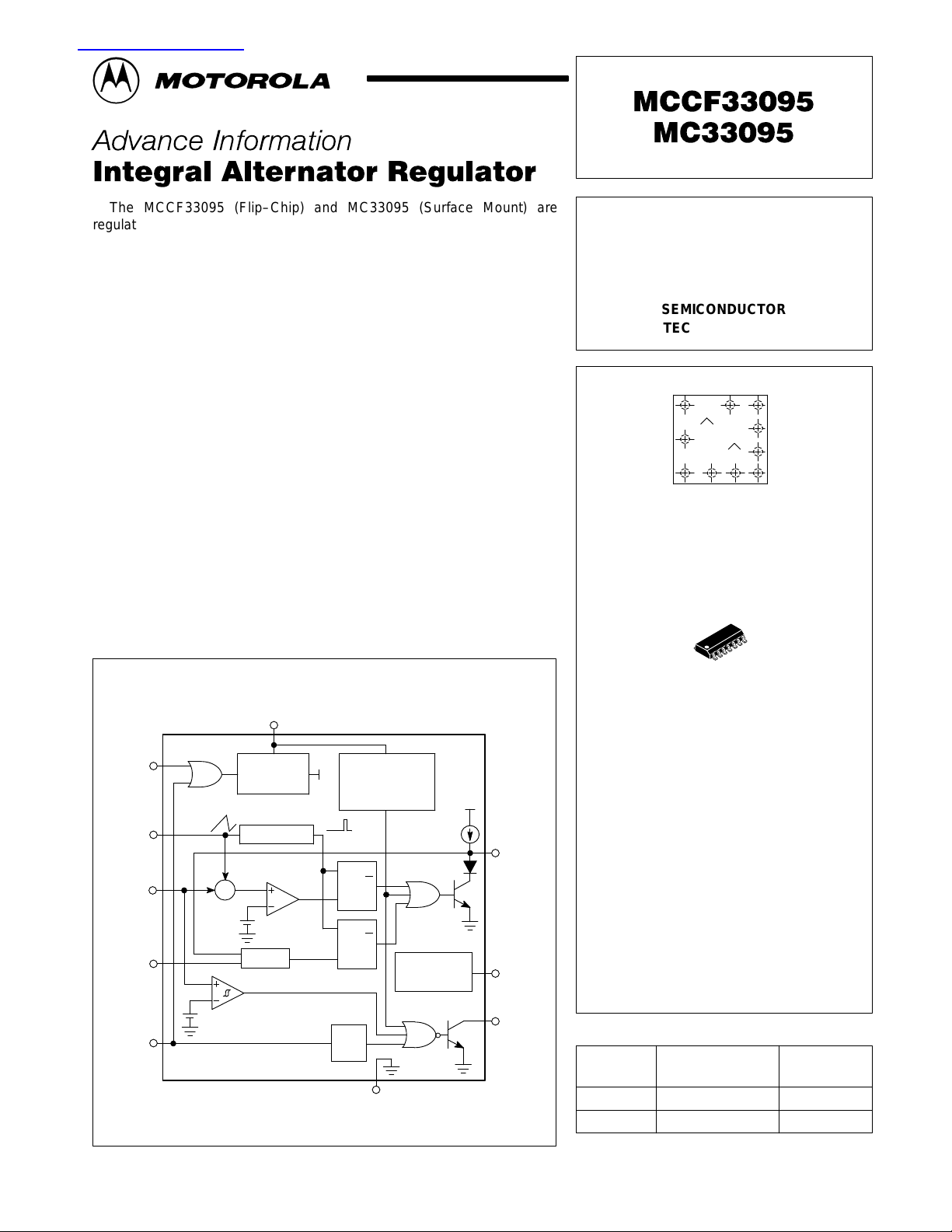
The MCCF33095 (Flip–Chip) and MC33095 (Surface Mount) are
regulator control integrated circuits designed for use in automotive 12 V
alternator charging systems. Few external components are required for full
system implementation. These devices provide control for a broad range of
12 V alternator charging systems when used in conjunction with the
appropriate Motorola Power Darlington transistor to control the field current
of the specific alternator.
Both versions have internal detection and protection features to withstand
extreme electrical variations encountered in harsh automotive environments.
Flip–Chip Technology allows the MCCF33095 to operate at higher ambient
temperatures than the surface mount version in addition to withstanding
severe vibration and thermal shock with a high degree of reliability .
• Constant Frequency with Variable Duty Cycle Operation
• Adjusts System Charging to Compensate for Changes
in Ambient Temperature
• Slew Rate Control to Reduce EMI
• Lamp Pin to Indicate Abnormal Operating Conditions
• Shorted Field Protection
• Resumes Normal Operation Once Fault Condition Ceases
• Operation from –40°C to 170°C for Flip–Chip and –40°C to 125°C
for SO–14
• Surface Mount or Solder Bump Processed Flip–Chip Assembly Versions
INTEGRAL
ALTERNATOR
REGULATOR
SEMICONDUCTOR
TECHNICAL DATA
123
4
FLIP–CHIP CONFIGURATION
(Backside View)
Back marking is oriented as shown
10
9
8
765
4 (8)
Ignition
6 (4)
Oscillator
2 (11)
Sense
10 (14)
Short
Circuit
3 (10)
Stator
Simplified Block Diagram
V
CC
1 (12)
Series
Regulator
Oscillator
V
Reg
Timer
V
HV
This device contains 145 active transistors.
+
Detection and
S
R
S
R
One
Shot
Ground
Load Dump
Protection
Q
Q
Thermal
Protection
8 (2)
+
9 (1)
Darlington
Drive
7 (3)
Roll–Off
5 (5)
Lamp
14
1
D SUFFIX
PLASTIC PACKAGE
CASE 751A
(SO–14)
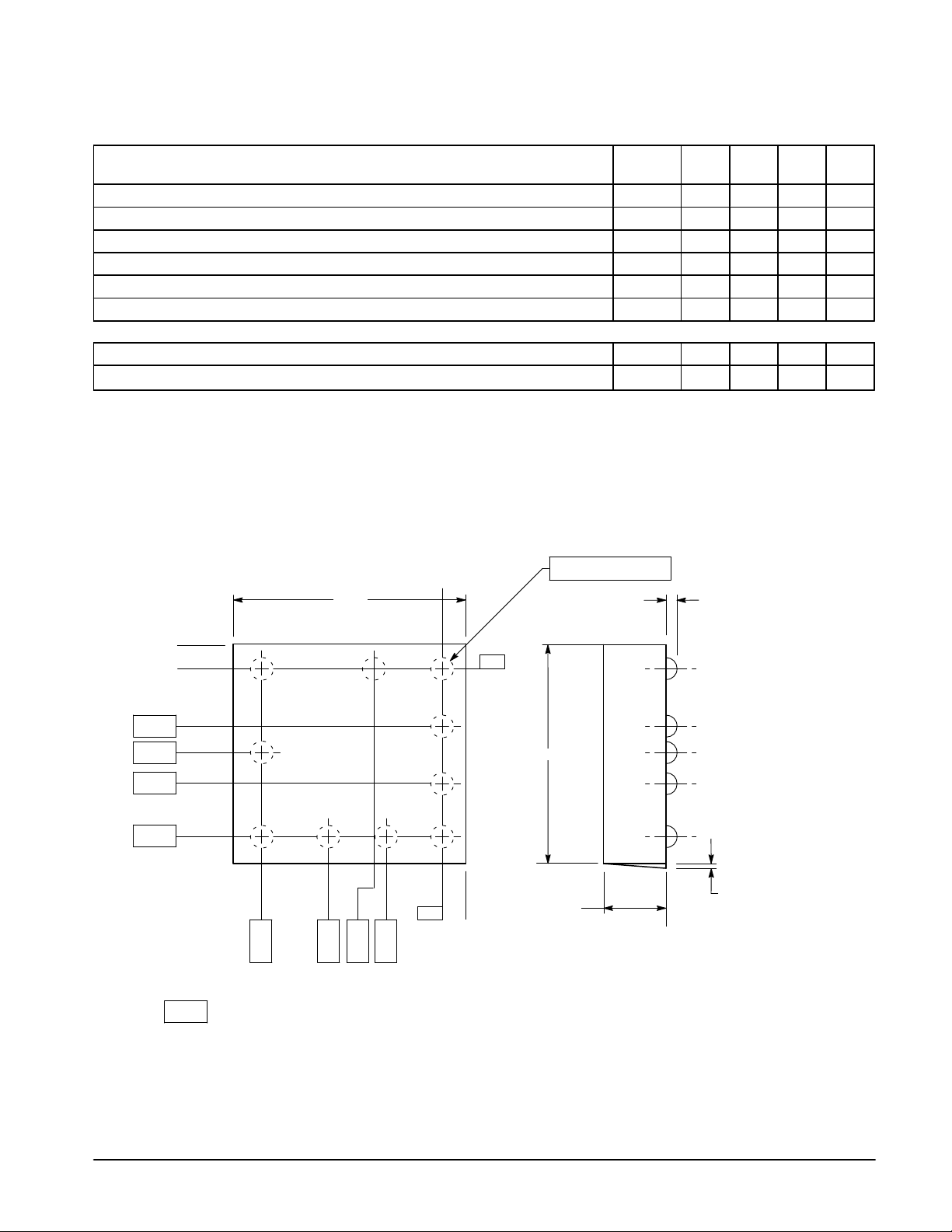
Bump Function SO–14 (Note 1)
1
2
3
4
5
6
7
8
9
10
NOTES: 1.No connections to Pins 3, 6, 7, 9 and 13.
2.Connected to ground internal to package.
V
CC
Sense
Stator
Ignition
Lamp
Oscillator
Roll–Off
Ground
Darlington Drive
Short Circuit
(12)
(11)
(10)
(3)(Note 2)
(14)
ORDERING INFORMATION
Operating
Device
MCCF33095
MC33095D
Temperature Range
TA = –40° to +170°C
TA = –40° to +125°C
Package
Flip–Chip
(8)
(5)
(4)
(2)
(1)
SO–14
This document contains information on a new product. Specifications and information herein
are subject to change without notice.
MOTOROLA ANALOG IC DEVICE DATA
Motorola, Inc. 1996 Rev 1
1
Page 2
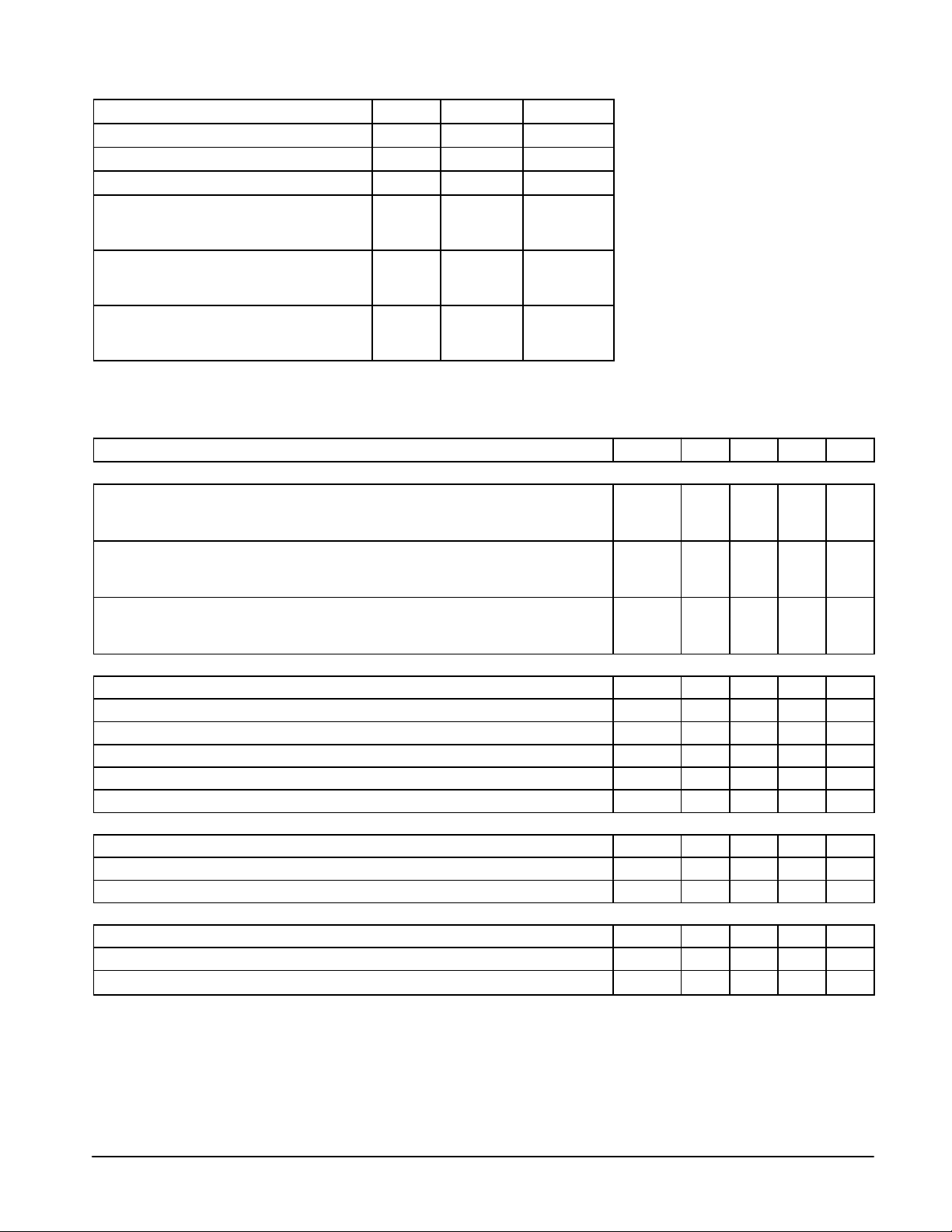
MCCF33095 MC33095
MAXIMUM RATINGS
Steady State VCC, V
VCC and V
Bump Shear Strength (Flip–Chip) – 8.0 Grams/Bump
Thermal Characteristics (Thermal Resistance)
Junction–to–Substrate (Flip–Chip)
Junction–to–Ambient (SO–14)
Junction Temperature
Flip–Chip
SO–14
Operating Ambient Temperature Range
Flip–Chip
SO–14
Transient – 80 V
IGN
ELECTRICAL CHARACTERISTICS (Limit values are given for –40°C ≤ T
(SO–14) and typical values represent approximate mean value at TA = 25°C. Oscillator, Roll–Of f, Ground, Short Circuit = 0 V,
and 12 V ≤ VCC, Sense, Stator, Ignition ≤ 16 V, unless otherwise specified.)
SUPPL Y (VCC)
Supply Current I
Disabled (Ignition = 0.5 V , Stator = 5.0 V) –50 0.2 300 µA
Enabled (VCC, Sense = 17 V, Ignition = 1.4 V) 0 3.9 25 mA
Darlington Drive Overvoltage V
Disable Threshold (VCC, Ignition, Short Circuit = 19 V to 29 V Ramp, Stator = 10 V) V
Hysteresis (VCC, Stator, Ignition, Short Circuit = 29 V to 19 V Ramp) V
Lamp Overvoltage V
Disable Threshold (VCC, Stator, Ignition, Short Circuit = 19 V to 29 V Ramp) V
Hysteresis V
SENSE
Sense Current (Oscillator = 2.0 V) I
Calibration Voltage (50% Duty Cycle) (Note 5) V
Lamp Comparator Detect Threshold V
Proportional Control Range M
Lamp Comparator Reset Threshold V
Lamp Hysteresis V
STATOR
Propagation Delay (Lamp–to–High, Stator = 15 V to 6.0 V) t
Reset Threshold Voltage (Lamp–to–Low, Stator = 5.0 V to 11 V) V
Input Current (Sense = 18 V , Oscillator = 2.0 V) I
LAMP
Saturation Voltage (Lamp = 14 mA) V
Leakage Current (Sense = 1.0 V , Lamp = 2.5 V) I
Saturation Voltage (VCC, Sense, Stator, Ignition = 30 V, Lamp = 20 mA) V
NOTES: 1.VCC applied through a 250 Ω resistor.
2.Sense input applied through a 100 kΩ and 50 kΩ resistor divider to generate one–third V
3.Stator and Ignition inputs applied through a 20 kΩ resistor.
4.Short Circuit input applied through a 30 kΩ resistor.
5.Oscillator pin connected in series with 0.022 µF capacitor to ground.
(Notes 1 and 3)
Rating
, V
IGN
STA
Characteristic
Symbol Value Unit
– 9.0 to 24 V
R
θJS
R
θJA
T
J
T
A
29
145
170
150
–40 to +170
–40 to +125
°C/W
°C
°C
≤ 150°C (Flip–Chip), –40°C ≤ TA ≤ 125°C
A
Symbol Min Typ Max Unit
CC
19 26 28.5
– 4.2 –
19 22.3 29.5
– 0.3 –
–10 0.6 10 µA
12.25 14.6 17.5 V
– 16.3 – V
50 187.4 350 mV
15.4 15.9 16.4 V
20 416.6 600 mV
6.0 59.4 600 ms
6.0 8.8 11 V
–10 1.5 10 µA
0 111.8 350 mV
–50 0.8 50 µA
0 147.4 350 mV
bat
CODD
CODDH
COL
COLH
SNS
R
SCD
V
HV
HYS
STA
IH
STA
OLL
OHL
OOLL
.
2
MOTOROLA ANALOG IC DEVICE DATA
Page 3
MCCF33095 MC33095
ELECTRICAL CHARACTERISTICS (continued) (Limit values are given for –40°C ≤ T
≤ 150°C (Flip–Chip), –40°C ≤ TA ≤ 125°C
A
(SO–14) and typical values represent approximate mean value at TA = 25°C. Oscillator, Roll–Of f, Ground, Short Circuit = 0 V,
and 12 V ≤ VCC, Sense, Stator, Ignition ≤ 16 V, unless otherwise specified.)
DARLINGTON DRIVE
Source Current (Pins VCC, Sense, Ignition = 9.0 V , Darlington Drive = V across
Power Darlington)
Saturation Voltage (Sense = 18 V, Oscillator = 2.0 V, Darlington Drive = –100 µA) V
I
OHDD
OLDD
Minimum “On” Time (Sense = 18 V) (Note 5) t
Frequency (Note 5) F
Minimum Duty Cycle (Sense = 18 V) (Note 5) DC
Rise Time (10% to 90%) (Note 5) t
Fall Time (90% to 10%) (Note 5) t
DD
OSC
DD
r
f
4.0 7.6 20 mA
0 300.1 350 mV
200 697.8 700 µs
75 174.7 325 Hz
4.0 12.2 13 %
10 21.4 50 µs
10 23.7 50 µs
SHORT CIRCUIT
Duty Cycle (Note 5) DC
“On” Time (Short Circuit High, Short Circuit = 8.0 V) (Note 5) PW
NOTES: 1.VCC applied through a 250 Ω resistor.
2.Sense input applied through a 100 kΩ and 50 kΩ resistor divider to generate one–third V
3.Stator and Ignition inputs applied through a 20 kΩ resistor.
4.Short Circuit input applied through a 30 kΩ resistor.
5.Oscillator pin connected in series with 0.022 µF capacitor to ground.
bat
.
SC
SC
1.0 1.7 5.0 %
60 99 660 µs
Figure 1. Flip–Chip Mechanical Dimensions
0.185
0.510
0.741
1.015
1.503
0.216
Dia. 10 Places
φ
0.127
0
2.032
3
0
12
–A–
0.025R of True Position
0.140
0.050 10 Places
10
4
1.905
9
0.029
Maximum taper either
direction allowed, 4 edges.
Die sawed through.
1.605
1.012
0.606
765
0.506
–B–
8
0.559
0.483
0
0.189
NOTES: 1.All dimensions shown indicated in millimeters.
2. Denotes basic dimension having zero
tolerance and describes the theoretical
exact location (true position) or contour.
MOTOROLA ANALOG IC DEVICE DATA
3
Page 4
MCCF33095 MC33095
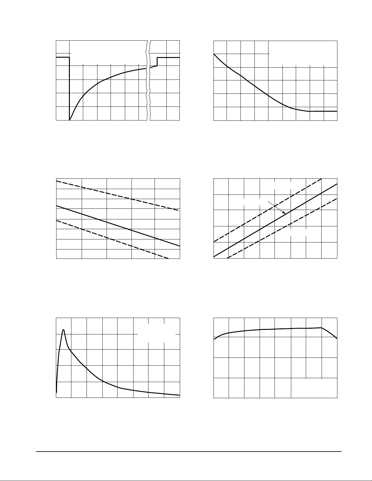
Figure 2. Pins 1, 3 and 4 Field Transient Decay Figure 3. Pins 1 and 4 Load Dump Transient Decay
40
20
0
VFT = 14.5 V for 0 ≥ t ≥ 0.38 sec
VFT = – 75 e
Refer to Notes 1 to 5 of Electrical Table
14.5 V
for Circuit Hook–Up
t/0.038
for 0
≤
t ≤ 0.38 sec
80
60
VLD = 80 e
VLD = 14.5 V for t
Refer to Notes 1 to 5 of Electrical
Table for Circuit Hook–Up
–5t
for 0 ≤ t ≤ 0.342 sec
≥
0.342 sec
, TRANSIENT FIELD VOLTAGE (V)
V
, VOLTAGE FOR 50% DUTY CYCLE (V)
V
FT
bat
–20
–40
–60
–75
16.5
16.0
15.5
15.0
14.5
14.0
13.5
13.0
12.5
–20
0 20 80 100 380 400
40 60
t, TIME (ms)
Figure 4. T emperature versus
V
for 50% Duty Cycle
bat
Maximum
Typical
Minimum
–40
0 40 80 120 160
TA, TEMPERATURE (
°
C)
420
40
, TRANSIENT VOL TAGE (V)
20
LD
V
0
0
19
18
17
16
15
, REQUIRED TO TURN–ON LAMP (V)
bat
V
14
12.5
100 300 400
Figure 5. V
Typical Ratio (1.13)
13 13.5 14 14.5 15 16.515.5 16
V
bat
200
t, TIME (ms)
(50% Duty Cycle) versus
bat
V
(Lamp “On”)
bat
Maximum Ratio (1.19)
Minimum Ratio (1.08)
FOR A 50% DUTY CYCLE (V)
, FIELD CURRENT (A)
F
I
4
1.025
1.000
0.075
0.050
0.025
Figure 6. Field Current versus Cycle Time Figure 7. Field Current versus Time
2.0
V
= 14.4 V
bat
Duty Cycle = 6.0%
°
C
TA = 25
0
0
1.4 2.8 4.2 5.6
SC, CYCLE TIME (ms)
, FIELD CURRENT (A)
F
I
1.5
1.0
0.5
0
0
1.4 2.8 5.64.2
SC, CYCLE TIME (ms)
MOTOROLA ANALOG IC DEVICE DATA
V
= 14.4 V
bat
Duty Cycle = 86%
°
C
TA = 25
Page 5
0.047
0.022
50 k
100 k
0.022
2 (11)
6 (4)
1 (12)
V
CC
SENSE
OSC
IGN
250
20 k
MCCF33095 MC33095
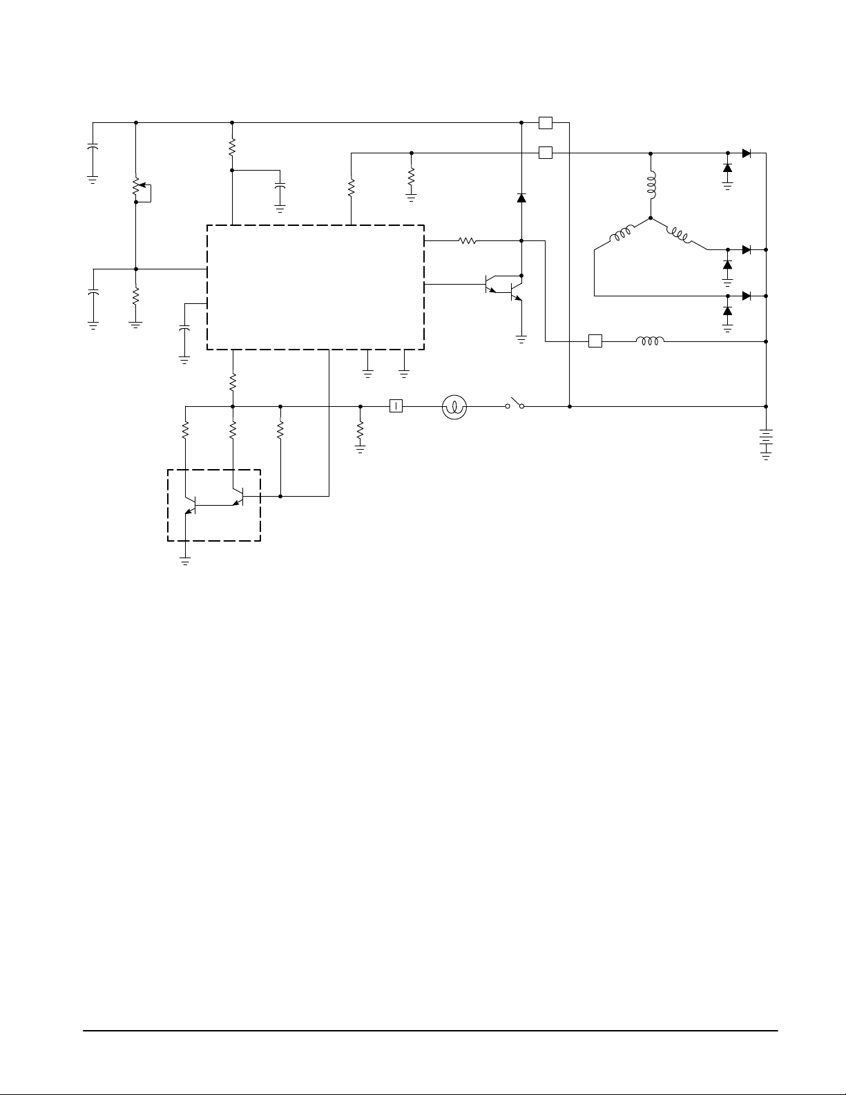
Figure 8. Integral Alternator Regulator System
Ω
8 (2)7 (7)5 (5)4 (8)
SC
DD
GND
1.0 k
10 (4)
9 (1)
30 k
Power Ground
0.1
MCCF33095
18 k
3 (10)
STATOR
ROLMP
A
S
Stator
Field
F
10
Ω
1.0 k
C1C2
E
2.4 k
B
1.5 k
Lamp
Ignition
Battery
MOTOROLA ANALOG IC DEVICE DATA
5
Page 6

MCCF33095 MC33095
FUNCTIONAL DESCRIPTION
Introduction
This ignition control circuit was originally designed and
offered as an MCCF33095 Flip–Chip for use in 12 V
automotive alternator charging systems. The MCCF33095
consists of many protection features which are entailed in a
ten pin flip–chip package. The device was subsequently
made available in a 14 pin surface mount version
(MC33095D). Both versions perform in a similar manner. The
Flip–Chip version has an advantage over the surface mount
version where minimized space and higher operating
ambient temperatures are of major concern. Device
operation and application suggestions for both versions are
given below.
Oscillator
The oscillator frequency is determined by the value of an
external capacitor from the Oscillator pin to ground (see
applications circuit). The oscillator frequency in a typical
application is approximately 175 Hz, but a range of 50 Hz to
500 Hz can reasonably be used. The waveform generated
consists of a positive linear slope followed by relatively fast
negative fall (sawtooth). The flip–flops are reset by the falling
edge of the sawtooth signal as shown on the logic diagram.
The oscillator signal peaks at approximately 3.0 V and
provides the timing required for the device.
Ignition
The Ignition input signal enables the device turn–on when
the Ignition pin voltage is greater than 1.4 V. This signal
normally originates from the ignition switch of automotive
systems.
Sense
The Sense pin functions as a voltage sensor. It
proportionally senses the battery voltage and determines the
amount of time the Darlington transistor is high over the next
cycle. A low voltage at the Sense pin will result in a long duty
cycle for the Darlington while a high voltage produces a short
duty cycle. In the application, proportional control is used to
determine the duty cycle. Proportional control is defined as
the sense ratio of battery voltage, present on the Sense pin,
required to obtain a 20% to 95% duty cycle range in the
application. The 20% duty cycle value will correlate to the
maximum battery in the application. Normally the sense ratio
of battery voltage is an end product trim adjustment.
Lamp
The Lamp output pin functions as a warning indicator for
overvoltage and stopped engine or broken belt conditions
existing in the system.
Stator
The Stator pin senses the voltage from the stator in the
application circuit, and keeps the device powered up while
the stator voltage is high. Furthermore, it acts as a sense for
a stopped engine or broken belt condition. If this condition is
detected, the Stator turns “on” the Lamp.
Power Supply, V
The VCC pin powers the entire device and disables all
outputs during any overvoltage condition.
Roll–Off
The Roll–Off pin provides thermal protection for the circuit.
This capability exists, but has not been characterized and is
not tested for at this time. Therefore, it is recommended that
this pin be connected to ground. The surface mount version
has this pin internally connected to ground.
Darlington Drive
The purpose of the Darlington Drive output pin is to turn on
an external power Darlington transistor. The Sense pin
voltage determines the duty cycle of the Darlington. The
oscillator is set to maintain a minimum duty cycle, except
during overvoltage and short circuit conditions.
Short Circuit
The Short Circuit pin monitors the field voltage. When the
Darlington Drive and Short Circuit pins are simultaneously
high for a duration greater than the slew rate period, a short
circuit condition is noted. The detection time required
prevents the device from reacting to false shorts. As a result
of short circuit detection, the output is disabled. During a short
circuit condition, the device automatically retries with a 2%
duty cycle (Darlington “on” time). Once the short circuit
condition ceases, normal device operation resumes.
Application Notes
A capacitor should be used in parallel with the VCC pin to
filter out noise transients on the supply or battery line.
Likewise, a capacitor should be used in parallel with the
Sense pin to create a dominant closed loop pole. Resistors
connected to inputs, as mentioned in Notes 1 through 5 of the
Electrical Characteristic table, should be used.
CC
6
MOTOROLA ANALOG IC DEVICE DATA
Page 7
MCCF33095 MC33095
FLIP–CHIP APPLICATION INFORMATION
Introduction
Although the packaging technology known as “flip–chip”
has been available for some time, it has seen few
applications outside the automotive and computer industries.
Present microelectronic trends are demanding smaller chip
sizes, reduced manufacturing costs, and improved reliability.
Flip–chip technology satisfies all of these needs.
Conventional assembly techniques involve bonding wires
to metal pads to make electrical contact to the integrated
circuit. Flip–chip assembly requires further processing of the
integrated circuit after final nitride deposition to establish
robust solder bumps with which to make electrical contact to
the circuit. A spatially identical solderable solder bump
pattern, normally formed on ceramic material, serves as a
substrate host for the flip–chip. The “bumped” flip–chip is
aligned to, and temporarily held in place through the use of
soldering paste. The aligned flip–chip and substrate host are
placed into an oven and the solder reflowed to establish both
electrical and mechanical bonding of the flip–chip to the
substrate circuit. Use of solder paste not only holds the chip
in temporary placement for reflow but also enhances the
reflow process to produce highly reliable bonds.
Flip–Chip Benefits
Some of the benefits of flip–chip assembly are:
1) Higher circuit density resulting in approximately
one–tenth the footprint required of a conventional
plastic encapsulated device.
2) Improved reliability, especially in high temperature
applications. This is due, in part, to the absence
of wires to corrode or fatigue from extensive
thermal cycling.
3) No bond wires are required that might possibly
become damaged during assembly.
4) Adaptable for simultaneous assembly of multiple
flip–chips, in a hybrid fashion, onto a single
ceramic substrate.
The following discussion covers the flip–chip process
steps performed by Motorola, and the assembly processing
required by the customer, in order to attach the flip–chip onto
a ceramic substrate.
MOTOROLA ’S FLIP–CHIP PROCESS
Overview
The process steps to develop an integrated circuit
flip–chip are identical to that of conventional integrated
circuits up to and including the deposition of the final nitride
passivation layer on the front surface (circuit side). At this
stage all device metal interconnects are present.
The process sequence is as follows:
1) Passivation–nitride photoresist and etch
2) Bimetal sputter (titanium (Ti) and tungsten (W)
followed by copper (Cu))
3) Photo mask to define the bump area
4) Copper plate
5) Lead plate
6) Tin plate
7) Photoresist clean to remove all photoresist material
8) Bimetal etchback
9) Reflow for bump formation
10) Final inspection
The diagram below depicts the various layers involved in
the bump process.
Figure 9. Plated Bump Structure
and Process Flow
Solder Bump Before Reflow
Plated Copper
Photoresist
Sputtered Cu
Sputtered TiW
Passivation Nitride
Al–Cu Metal Pad
Solder Bump After Reflow
Plated Copper
Photoresist
Sputtered Cu
Sputtered TiW
Passivation Nitride
Al–Cu Metal Pad
Initially, photoresist techniques are used to create
openings in the nitride passivation layer exposing the metal
pad bias. Ti/W, followed by Cu, are sputtered across the
entire wafer surface. The surface is then photo patterned to
define the bump areas. The sputtered metals together
constitute a base metal for the next two metal depositions.
The Ti/W layer provides excellent intermetallic adhesion
between the metal pads and the sputtered copper. In
addition, the Ti/W provides a highly reliable interface to
absorb mechanical shock and vibrations frequently
encountered in automotive applications. The sputtered
copper layer creates a platform onto which an electroplated
copper layer can be built–up. Layers of Cu, Pb, and Sn are
applied by plating onto the void areas of the photoresist
material. The photoresist is then removed and the earlier
sputtered materials are etched away. The flip–chip wafer is
then put into an oven exposing it to a specific ambient
temperature which causes the lead and tin to ball–up and
form a solder alloy .
IC Solder Bumps
The solder consists of approximately 93% lead and 7% tin.
The alloying of lead with tin provides a bump with good
ductility and joint adhesion properties. Precise amounts of tin
are used in conjunction with lead. Too much tin in relation to
lead can cause the solder joints to become brittle and subject
to fatigue failure. Motorola has established what it believes to
be the optimum material composition necessary in order to
achieve high bump reliability .
In the make–up of the flip–chip design, bumps are ideally
spaced evenly and symmetrically along each edge of the
chip allowing for stress experienced during thermal
expansion and vibration to be distributed evenly from bump
to bump. The bump dimensions and center–to–center
spacing (pitch) are specified by the chip layout and the
specific application. The nominal diameter of the bumps is
6.5 mils and the minimum center–to–center pitch is roughly
8.0 mils.
MOTOROLA ANALOG IC DEVICE DATA
7
Page 8

MCCF33095 MC33095
Reflow
The reflow process creates a thermally induced amalgam
of the lead and tin. In the melting process, the surface tension
is equalized causing the melted solder to uniformly ball up as
mentioned earlier.
The ideal reflow oven profile gradually ramps up in
temperature to an initial plateau. The purpose of the plateau
is to establish a near equilibrium temperature just below that
of the solder’s melting temperature. Following the preheat, a
short time and higher temperature excursion is necessary.
This is to ensure adequate melting of the solder materials.
The temperature is then ramped down to room temperature.
An atmosphere of hydrogen is used during the reflow heat
cycle. The hydrogen provides a reducing atmosphere for the
removal of any surface oxides present. The formation or
presence of oxides can cause degradation in the bond
reliability of the product.
During the flip–chip attachment reflow onto the ceramic
substrate host, the created surface tension of the molten
solder aids in the alignment of the chip onto the ceramic
substrate.
Reliability
Motorola is determined to bring high quality and reliable
products to its customers. This is being brought about by
increased automation, in–line Statistical Process Control
(SPC), bump shear strength testing, thermocycling from
–40° to +140°C, process improvements such as backside
laser marking of the silicon chip, and improved copper
plating techniques.
substrate from external moisture. A commonly used gel for
this purpose is Dow Corning 562. As a final module assembly
step, a cover is recommended to be placed over the ceramic
assembly for further protection of the circuit.
It should be pointed out that the commonly used ceramic
substrate material, though more expensive than other
substrate materials, offers significantly superior thermal
properties. By comparison, the use of ceramic material offers
33 times the thermal advantage of the second best material,
Ceracom. The common FR–4 epoxy material is 100 times
less thermally conductive than ceramic. For applications
where dielectric constants are important and/or heat
dissipation is not of real importance, other less costly
materials can be used. The basic concept of the process is
identical for all flip–chip substrates used.
Figure 10. Process Flow Diagram
Printed Circuit
Board (PCB)
Bumped Chip
Bumping PCB
Bumped PCB
on Pallet
Chip Placement
IR Reflow
ATTACHING FLIP–CHIPS ONTO
CERAMIC SUBSTRA TES
Overview
The assembly or process of attaching the flip–chip onto a
ceramic substrate is performed by the module fabricator.
Prior to actual assembly, the ceramic substrate should
undergo several process steps. Care should be exercised to
properly orient the flip–chip onto the substrate host in order to
accommodate the appropriate solder bumps. Ideally, the
flip–chip should be removed from the waffle pack with a pick
and place machine utilizing a vacuum pick–up to move the
die onto the ceramic substrate. Any other components to be
reflow soldered onto the substrate can be placed onto the
substrate in a similar manner. Flip–chip assembly onto a
ceramic substrate allows for some passive components,
such as resistors, to be formed directly into the ceramic
substrate circuit pattern itself. With all surface components to
be mounted in place on the ceramic substrate, the assembly
is moved into the furnace where it undergoes a specified
temperature variation to solder all the components onto the
ceramic substrate. This is accomplished by melting
(reflowing) the substrate solder bumps. The resulting
assembly should, after being cooled, be cleaned to remove
any flux residues. If the substrate assembly is to be mounted
into a module, it is recommended that the cavity of the
module be filled with an appropriate silicon gel. The use of a
gel coating helps to seal the individual components on the
Cleaning
Encapsulation
Ceramic Substrate Preparation
The recommended ceramic substrate is aluminum oxide.
These substrates come connected in what is referred to as a
card. This is identical to the concept of die or chips on a wafer.
Each card usually contains 8 to 16 substrates.
Initially, the ceramic should be precleaned with isopropyl
alcohol, followed by freon. The bump pattern is then
transferred onto the substrate using a metal stencil technique
using a palladium silver conducting paste, such as DuPont
9476, through a #325 mesh. Once the pattern is applied, the
substrate is dried for ten minutes at 150°C and then fired for
60 minutes at a temperature increasing to a peak of 850°C for
ten additional minutes. Solder paste is then stenciled onto
the pads.
A metal etched stencil defining the contact areas is
recommended. The use of an etched stencil affords better
solder paste control than does a silk screen. The metal stencil
affords a deposition of a known amount of solder paste,
thereby preventing bridging caused by excess solder usage.
8
MOTOROLA ANALOG IC DEVICE DATA
Page 9
MCCF33095 MC33095
Solder Paste Content
It is recommended that the solder paste consist of 10% tin,
88% lead, and 2% silver alloy . However , 95/3/2 compositions
have had successful results.
A rosin based flux, such as RMA (Rosin Mildly Activated)
manufactured by Dupont and having spherical particles of 45
to 75 microns, should be used. The tackiness of the solder
paste at room temperature helps to hold the flip–chip in place
during the pick and place operation. The use of flux:
1) Prevents excess oxidation during reflow.
2) Optimizes the flow of liquid solder through the stencil.
3) Smooths the surface by reducing surface tension, and
4) Enhances the normalization of surface tension upon
reflow causing the flip–chip bumps to effectively
auto–align themselves to substrate bump pads.
A solder mask can be used for applications requiring high
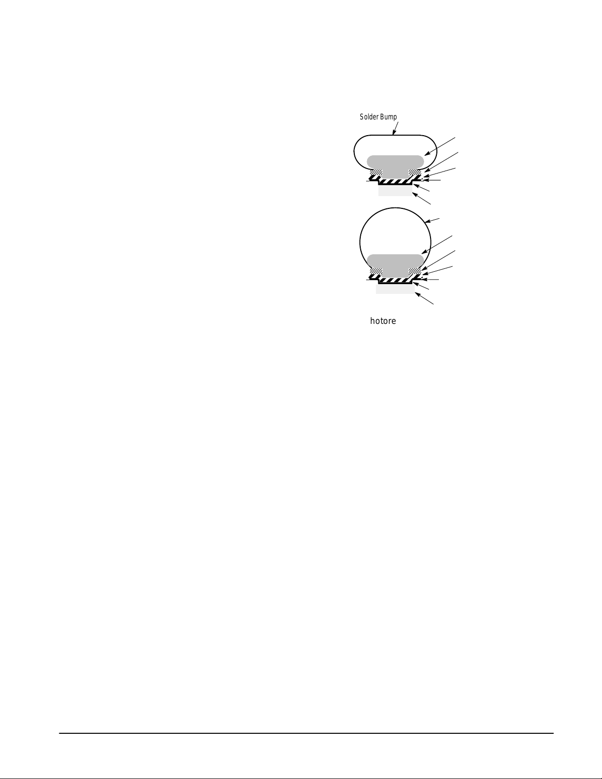
precision as shown in Figures 1 1a and 11b.
to some intermediate temperature point for annealing
purposes.
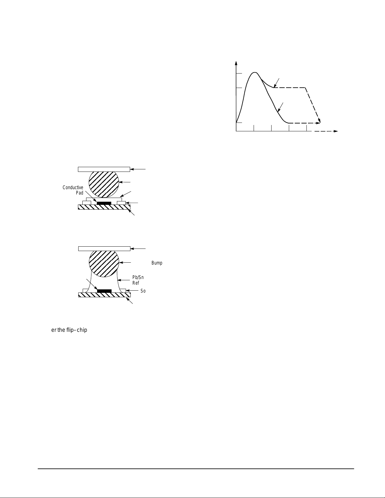
Figure 12. Reflow Oven Profile
Additional
350
°
300
, TEMPERATURE ( C)
A
T
Annealing
Profile
Standard
Profile
129603
t, TIME (MINUTES)
Figure 11.
Figure 11a. Before Reflow
Conductive
Pad
IC
Flip–Chip Bump
Flattened Pb/Sn
Solder Mask
Ceramic
Figure 11b. After Reflow
IC
Flip–Chip Bump
Conductive
Pad
Pb/Sn
Reflow
Solder Mask
Ceramic
Oven Profile
After the flip–chip is placed onto the bumped substrate, the
substrate and flip–chip are ready for reflow. Initially, the
flip–chip is heated to a peak temperature of around 300° to
350°C for five minutes. It is to be noted that the flip–chip
bumps have a higher melting temperature than the bumps on
the substrate. During assembly reflow, the substrate bumps
melt and create a substrate to flip–chip bump bond. After
reflow, the assembled part is cooled to room temperature or
The oven temperature profile is established primarily to
melt the solder while minimizing the alloying of the materials
and keeping the flux from boiling away . It should be noted that
when the flip–chip is placed onto the substrate, the material is
stressed in one direction or another. The use of flux helps to
reduce any surface stresses present. A reduction in the
surface stress enhances solder wetting which in turn aids in
the alignment of the flip–chip to the substrate. Poor solder
wetting will produce misalignment as well as inferior bond
strengths and reliability .
It is recommended that an inert atmosphere such as
nitrogen be used during the reflow process to prevent
oxidation.
Final Cleaning
The final cleaning involves removing the remaining flux
from the flip–chip assembly. Three possible methods of
removing flux are: ultrasonic cleaner, Terpene solvent and DI
water, or vapor degreaser. The flux manufacturer should be
able to recommend the proper type of vapor degreaser to be
used.
T est and Reliability
Both visual inspection and shear strength testing should
be performed on packaged flip–chip assemblies.
Solder reflow results that exhibit a grainy and dull
appearance produce inferior bond shear strengths. Inferior
bond shear strengths are visually recognizable by:
1) The presence of old or badly oxidized solder paste.
2) Insufficient amount of solderable material.
3) The contamination of bond pads with grease, oil, etc.
It should be mentioned that many contaminants are
transparent and not easily detectable by visual means.
MOTOROLA ANALOG IC DEVICE DATA
9
Page 10

MCCF33095 MC33095
Shear strength testing should meet a 0.8 Newtons/Bump
criteria. Shear strength testing should follow thermocycling of
the chip from – 40° to +140°C to insure the stability of shear
strength over temperature. Figure 13 depicts a test set–up
which might possibly be used.
Figure 13. Shear T est Fixture
Substrate
Flip–Chip
Cantilever Arm
Aside from physical contamination, flip–chips, like any
other chips, should not be handled directly due to the fact that
electrostatic discharges can cause permanent damage to the
electronic circuit. Flip–chips which do survive an electrostatic
discharge can be left in a weakened condition resulting in
reduced reliability of the end product. To avoid electrostatic
damage of the circuit, assembly personnel should make use
of a wrist strap or some other device to provide electrostatic
grounding of their body. For the same reason, machinery
used to assemble semiconductor circuits should be
electrostaticly grounded.
Flip–chips rely primarily on the thermal path established by
the bumps to remove heat from the chip as a result of internal
circuit operation. Standard Motorola flip–chips have a thermal
resistance of approximately 290°C/W/Bump. This figure can
be used to estimate the allowed maximum power dissipation
of the chip.
Cost and Equipment Manufacturers
The cost of implementing a flip–chip assembly process
depends on the specific production requirements and as a
result will vary over a broad range. It is possible to implement
a small volume laboratory set–up for a few hundred dollars
using manual operations. At the other end of the scale one
could spend millions setting up a fully automated line
incorporating pattern recognization, chip and substrate
orientation, reflow, cleaning, and test. The module fabricator
will have to make this assessment.
An assembly operator can manually accomplish the pick
and place operation using a vacuum probe to pick–up and
orient the flip–chip onto the substrate. Furthermore, it is
possible to perform the reflow assembly operation using a
simple batch process oven fabricated from a laboratory hot
plate. However, the use of such process techniques will have
questionable impact on the final product’s reliability and
quality. For this reason, it is highly recommended that the
module fabricator seriously consider two major pieces of
equipment; a pick and place machine and an infrared solder
reflow oven. Both pieces of equipment can vary over a wide
cost range depending on the production requirements. A
partial list of manufacturers for this equipment is given below.
Pick and Place Machine:
Universal Instruments Corp.
Dover Technologies, Inc.
Binghamton, NY 13902
(607) 772–7522
Seiko
Torrance, CA 90505
(310) 517–7850
Laurier Inc.
Hudson, NH 03051
(603) 889–8800
Infrared Reflow Oven:
BTU
Bellerica, MA 01862
(508) 667–41 11
Vitronics
Newmarket, NH 03857
(603) 659–6550
Additional Applications
Completed ceramic flip–chip sub–assemblies can be
stacked one on top of another to produce an overall
assembly by making contact connections through bumps.
This technology is beginning to emerge in the computer
industry where physical module size is of significant
importance. Furthermore, this assembly technology, though
more complex, is undergoing serious consideration within the
automotive industry as well.
Applications requiring small size and high reliability at high
ambient temperatures can benefit considerably through the
implementation of flip–chip assembly techniques.
10
MOTOROLA ANALOG IC DEVICE DATA
Page 11
–T–
SEATING
PLANE
–A–
14 8
G
D 14 PL
0.25 (0.010) A
MCCF33095 MC33095
OUTLINE DIMENSIONS
D SUFFIX
PLASTIC PACKAGE
CASE 751A–03
(SO–14)
ISSUE F
–B–
P
7 PL
M
71
0.25 (0.010) B
C
X 45
R
K
M
S
B
T
S
M
_
M
J
NOTES:
1. DIMENSIONING AND TOLERANCING PER
ANSI Y14.5M, 1982.
2. CONTROLLING DIMENSION: MILLIMETER.
3. DIMENSIONS A AND B DO NOT INCLUDE
MOLD PROTRUSION.
4. MAXIMUM MOLD PROTRUSION 0.15 (0.006)
PER SIDE.
5. DIMENSION D DOES NOT INCLUDE DAMBAR
PROTRUSION. ALLOWABLE DAMBAR
PROTRUSION SHALL BE 0.127 (0.005) TOTAL
IN EXCESS OF THE D DIMENSION AT
MAXIMUM MATERIAL CONDITION.
F
DIM MIN MAX MIN MAX
A 8.55 8.75 0.337 0.344
B 3.80 4.00 0.150 0.157
C 1.35 1.75 0.054 0.068
D 0.35 0.49 0.014 0.019
F 0.40 1.25 0.016 0.049
G 1.27 BSC 0.050 BSC
J 0.19 0.25 0.008 0.009
K 0.10 0.25 0.004 0.009
M 0 7 0 7
____
P 5.80 6.20 0.228 0.244
R 0.25 0.50 0.010 0.019
INCHESMILLIMETERS
MOTOROLA ANALOG IC DEVICE DATA
11
Page 12

MCCF33095 MC33095
Motorola reserves the right to make changes without further notice to any products herein. Motorola makes no warranty , representation or guarantee regarding
the suitability of its products for any particular purpose, nor does Motorola assume any liability arising out of the application or use of any product or circuit, and
specifically disclaims any and all liability, including without limitation consequential or incidental damages. “T ypical” parameters which may be provided in Motorola
data sheets and/or specifications can and do vary in different applications and actual performance may vary over time. All operating parameters, including “Typicals”
must be validated for each customer application by customer’s technical experts. Motorola does not convey any license under its patent rights nor the rights of
others. Motorola products are not designed, intended, or authorized for use as components in systems intended for surgical implant into the body, or other
applications intended to support or sustain life, or for any other application in which the failure of the Motorola product could create a situation where personal injury
or death may occur. Should Buyer purchase or use Motorola products for any such unintended or unauthorized application, Buyer shall indemnify and hold Motorola
and its officers, employees, subsidiaries, affiliates, and distributors harmless against all claims, costs, damages, and expenses, and reasonable attorney fees
arising out of, directly or indirectly, any claim of personal injury or death associated with such unintended or unauthorized use, even if such claim alleges that Motorola
was negligent regarding the design or manufacture of the part. Motorola and are registered trademarks of Motorola, Inc. Motorola, Inc. is an Equal
Opportunity/Affirmative Action Employer.
How to reach us:
USA/EUROPE/Locations Not Listed: Motorola Literature Distribution; JAP AN: Nippon Motorola Ltd.; Tatsumi–SPD–JLDC, 6F Seibu–Butsuryu–Center,
P.O. Box 20912; Phoenix, Arizona 85036. 1–800–441–2447 or 602–303–5454 3–14–2 Tatsumi Koto–Ku, Tokyo 135, Japan. 03–81–3521–8315
MFAX: RMF AX0@email.sps.mot.com – TOUCHT ONE 602–244–6609 ASIA/PACIFIC: Motorola Semiconductors H.K. Ltd.; 8B Tai Ping Industrial Park,
INTERNET: http://Design–NET.com 51 Ting Kok Road, Tai Po, N.T., Hong Kong. 852–26629298
12
◊
MOTOROLA ANALOG IC DEVICE DATA
MCCF33095/D
*MCCF33095/D*
 Loading...