

Page 1
T
40° t
85°C
查询MC33035/D供应商
The MC33035 is a high performance second generation monolithic
brushless DC motor controller containing all of the active functions required
to implement a full featured open loop, three or four phase motor control
system. This device consists of a rotor position decoder for proper
commutation sequencing, temperature compensated reference capable of
supplying sensor power, frequency programmable sawtooth oscillator, three
open collector top drivers, and three high current totem pole bottom drivers
ideally suited for driving power MOSFETs.
Also included are protective features consisting of undervoltage lockout,
cycle–by–cycle current limiting with a selectable time delayed latched
shutdown mode, internal thermal shutdown, and a unique fault output that
can be interfaced into microprocessor controlled systems.
Typical motor control functions include open loop speed, forward or
reverse direction, run enable, and dynamic braking. The MC33035 is
designed to operate with electrical sensor phasings of 60°/300° or
120°/240°, and can also efficiently control brush DC motors.
• 10 to 30 V Operation
• Undervoltage Lockout
• 6.25 V Reference Capable of Supplying Sensor Power
• Fully Accessible Error Amplifier for Closed Loop Servo Applications
• High Current Drivers Can Control External 3–Phase MOSFET Bridge
• Cycle–By–Cycle Current Limiting
• Pinned–Out Current Sense Reference
• Internal Thermal Shutdown
• Selectable 60°/300° or 120°/240° Sensor Phasings
• Can Efficiently Control Brush DC Motors with External MOSFET
H–Bridge
ORDERING INFORMATION
Operating
Device
MC33035DW
MC33035P
Temperature Range
°
A
= –
o +
°
Package
SO–24L
Plastic DIP
Order this document by MC33035/D
BRUSHLESS DC
MOTOR CONTROLLER
SEMICONDUCTOR
TECHNICAL DATA
P SUFFIX
PLASTIC PACKAGE
CASE 724
DW SUFFIX
PLASTIC PACKAGE
CASE 751E
(SO–24L)
PIN CONNECTIONS
Top Drive
Output
Sensor
Inputs
Output Enable
Reference Output
Current Sense
Noninverting Input
Noninverting Input
Inverting Input
B
T
A
T
S
A
S
B
S
C
Oscillator
Error Amp
Error Amp
24
1
24
1
2
3
4
5
6
7
8
9
10
11
1
C
24
T
23
Brake
22
°
/120°SelectFwd/Rev
60
A
21
B
20
B
B
19
C
B
18
V
C
17
V
CC
Gnd
16
Current Sense
15
Inverting Input
14
Output
Fault
Error Amp Out/
1312
PWM Input
Bottom
Drive
Outputs
(Top View)
MOTOROLA ANALOG IC DEVICE DATA
Motorola, Inc. 1998 Rev 3
1
Page 2
Fwd/Rev
60°/120
Enable
V
R
T
C
T
°
in
Speed
Set
Faster
22
17
18
11
12
13
10
4
5
6
3
7
8
Reference
Regulator
Error Amp
Oscillator
Undervoltage
Lockout
PWM
MC33035
Representative Schematic Diagram
Rotor
Position
Decoder
Thermal
Shutdown
R
Q
S
S
Q
R
14
24
21
20
19
2
1
9
Fault
V
M
Output
Buffers
N
SS
N
Motor
2316
Brake
This device contains 285 active transistors.
15
Current Sense
Reference
2
MOTOROLA ANALOG IC DEVICE DATA
Page 3

MC33035
MAXIMUM RATINGS
Rating Symbol Value Unit
Power Supply Voltage V
Digital Inputs (Pins 3, 4, 5, 6, 22, 23) – V
Oscillator Input Current (Source or Sink) I
Error Amp Input Voltage Range
(Pins 11, 12, Note 1)
Error Amp Output Current
(Source or Sink, Note 2)
Current Sense Input Voltage Range (Pins 9, 15) V
Fault Output Voltage V
Fault Output Sink Current I
Top Drive Voltage (Pins 1, 2, 24) V
Top Drive Sink Current (Pins 1, 2, 24) I
Bottom Drive Supply Voltage (Pin 18) V
Bottom Drive Output Current I
(Source or Sink, Pins 19, 20, 21)
Power Dissipation and Thermal Characteristics
P Suffix, Dual In Line, Case 724
Maximum Power Dissipation @ TA = 85°C P
Thermal Resistance, Junction–to–Air R
DW Suffix, Surface Mount, Case 751E
Maximum Power Dissipation @ TA = 85°C P
Thermal Resistance, Junction–to–Air R
Operating Junction Temperature T
Operating Ambient Temperature Range T
Storage Temperature Range T
CC
OSC
V
IR
I
Out
Sense
CE(Fault
Sink(Fault)
CE(top)
Sink(top)
C
DRV
D
θJA
D
θJA
J
A
stg
–0.3 to V
–0.3 to 5.0 V
)
–40 to +85 °C
–65 to +150 °C
40 V
ref
30 mA
ref
10 mA
20 V
20 mA
40 V
50 mA
30 V
100 mA
867 mW
75 °C/W
650 mW
100 °C/W
150 °C
V
V
ELECTRICAL CHARACTERISTICS (V
Characteristic
REFERENCE SECTION
Reference Output Voltage (I
TA = 25°C
TA = –40° to +85°C
Line Regulation (VCC = 10 to 30 V, I
Load Regulation (I
Output Short Circuit Current (Note 3) I
Reference Under Voltage Lockout Threshold V
ERROR AMPLIFIER
Input Offset Voltage (TA = –40° to +85°C) V
Input Offset Current (TA = –40° to +85°C) I
Input Bias Current (TA = –40° to +85°C) I
Input Common Mode Voltage Range V
Open Loop Voltage Gain (VO = 3.0 V, RL = 15 k) A
Input Common Mode Rejection Ratio CMRR 55 86 – dB
Power Supply Rejection Ratio (VCC = VC = 10 to 30 V) PSRR 65 105 – dB
NOTES: 1. The input common mode voltage or input signal voltage should not be allowed to go negative by more than 0.3 V.
2.The compliance voltage must not exceed the range of –0.3 to V
3.Maximum package power dissipation limits must be observed.
= 1.0 to 20 mA) Reg
ref
= 1.0 mA)
ref
ref
= VC = 20 V, RT = 4.7 k, CT = 10 nF, TA = 25°C, unless otherwise noted.)
CC
Symbol Min Typ Max Unit
V
= 1.0 mA) Reg
.
ref
ref
line
load
SC
th
IO
IO
IB
ICR
VOL
5.9
5.82
– 1.5 30 mV
– 16 30 mV
40 75 – mA
4.0 4.5 5.0 V
– 0.4 10 mV
– 8.0 500 nA
– –46 –1000 nA
70 80 – dB
6.24
–
(0 V to V
6.5
6.57
) V
ref
V
MOTOROLA ANALOG IC DEVICE DATA
3
Page 4

MC33035
Output Enable
µA
gp (IH)
IH
Bottom Drive Output Voltage
V
g(
CC C source
)
OH
(
CC
)
(
CC
)
Power Supply Current
mA
Pin 17 (VCC VC 20 V)
I
CC
121416
(
CC
0,C30 )
0
(
CC C
)
C
ELECTRICAL CHARACTERISTICS (continued) (V
Characteristic
ERROR AMPLIFIER
Output Voltage Swing
High State (RL = 15 k to Gnd)
Low State (RL = 15 k to V
OSCILLATOR SECTION
Oscillator Frequency f
Frequency Change with Voltage (VCC = 10 to 30 V) ∆f
Sawtooth Peak Voltage V
Sawtooth Valley Voltage V
LOGIC INPUTS
Input Threshold Voltage (Pins 3, 4, 5, 6, 7, 22, 23)
High State
Low State
Sensor Inputs (Pins 4, 5, 6)
High State Input Current (VIH = 5.0 V)
Low State Input Current (VIL = 0 V)
Forward/Reverse, 60°/120° Select (Pins 3, 22, 23)
High State Input Current (VIH = 5.0 V)
Low State Input Current (VIL = 0 V)
Output Enable µA
High State Input Current (VIH = 5.0 V)
Low State Input Current (VIL = 0 V)
CURRENT–LIMIT COMPARATOR
Threshold Voltage V
Input Common Mode Voltage Range V
Input Bias Current I
OUTPUTS AND POWER SECTIONS
Top Drive Output Sink Saturation (I
Top Drive Output Off–State Leakage (VCE = 30 V) I
Top Drive Output Switching Time (CL = 47 pF, RL = 1.0 k) ns
Rise Time t
Fall Time t
Bottom Drive Output Voltage V
High State (VCC = 20 V, VC = 30 V, I
Low State (VCC = 20 V, VC = 30 V, I
Bottom Drive Output Switching Time (CL = 1000 pF) ns
Rise Time t
Fall Time t
Fault Output Sink Saturation (I
Fault Output Off–State Leakage (VCE = 20 V) I
Under Voltage Lockout V
Drive Output Enabled (VCC or VC Increasing) V
Hysteresis V
Power Supply Current mA
Pin 17 (VCC = VC = 20 V) I
Pin 17 (VCC = 20 V, VC = 30 V)
Pin 18 (VCC = VC = 20 V) I
Pin 18 (VCC = 20 V, VC = 30 V)
)
ref
= 25 mA) V
sink
= 50 mA)
source
= 50 mA)
sink
= 16 mA) V
sink
= VC = 20 V, RT = 4.7 k, CT = 10 nF, TA = 25°C, unless otherwise noted.)
CC
Symbol Min Typ Max Unit
V
OH
V
OL
OSC
/∆V – 0.01 5.0 %
OSC
OSC(P)
OSC(V)
V
IH
V
IL
I
IH
I
IL
I
IH
I
IL
I
IH
I
IL
th
ICR
IB
CE(sat)
DRV(leak)
r
f
V
OH
V
OL
r
f
CE(sat)
FLT(leak)
th(on)
H
CC
C
4.6
–
22 25 28 kHz
– 4.1 4.5 V
1.2 1.5 – V
3.0
–
–150
–600
–75
–300
–60
–60 –29 –10
85 101 115 mV
– 3.0 – V
– –0.9 –5.0 µA
– 0.5 1.5 V
– 0.06 100 µA
– 107 300
– 26 300
(VCC –2.0) (VCC –1.1)
–
– 38 200
– 30 200
– 225 500 mV
– 1.0 100 µA
8.2 8.9 10
0.1 0.2 0.3
– 12 16
–
– 3.5
– 5.0 10
5.3
0.5
2.2
1.7
–70
–337
–36
–175
–29
1.5 2.0
–
1.0
–
0.8
–20
–150
–10
–75
–10
–
20
6.0
V
V
µA
µA
4
MOTOROLA ANALOG IC DEVICE DATA
Page 5
MC33035
Figure 1. Oscillator Frequency versus
100
10
OSCILLA TOR FREQUENCY (kHz)
CT = 100 nF
,
OSC
f
0
1.0
Figure 3. Error Amp Open Loop Gain and
56
48
40
32
24
16
VCC = 20 V
8.0
VC = 20 V
VO = 3.0 V
0
–8.0
, OPEN LOOP VOL TAGE GAIN (dB)
–16
VOL
A
–24
RL = 15 k
CL = 100 pF
TA = 25
1.0 k
Timing Resistor
CT = 10 nF
RT, TIMING RESISTOR (k
Phase versus Frequency
Phase
Gain
°
C
f, FREQUENCY (Hz)
CT = 1.0 nF
Ω
)
VCC = 20 V
VC = 20 V
°
C
TA = 25
100010010
10 M1.0 M100 k10 k
Figure 2. Oscillator Frequency Change
4.0
VCC = 20 V
VC = 20 V
RT = 4.7 k
2.0
CT = 10 nF
0
–2.0
OSCILLA T OR FREQUENCY CHANGE (%)
,
OSC
–4.0
f
∆
–55
Figure 4. Error Amp Output Saturation
40
60
80
100
120
140
160
180
EXCESS PHASE (DEGREES)
,
200
φ
220
240
– 0.8
–1.6
, OUTPUT SA TURATION VOLTAGE (V)
sat
V
0
1.6
0.8
0
versus T emperature
TA, AMBIENT TEMPERATURE (°C)
V oltage versus Load Current
V
ref
Source Saturation
(Load to Ground)
Sink Saturation
Gnd
1.0 2.0
IO, OUTPUT LOAD CURRENT (mA)
(Load to V
ref
1007550250–25
VCC = 20 V
VC = 20 V
TA = 25
)
125
°
C
5.04.03.00
Figure 5. Error Amp Small–Signal
Transient Response
3.05
3.0
, OUTPUT VOL TAGE (V)
O
V
2.95
µ
s/DIV
1.0
MOTOROLA ANALOG IC DEVICE DATA
AV = +1.0
No Load
°
TA = 25
Figure 6. Error Amp Large–Signal
Transient Response
AV = +1.0
No Load
TA = 25
°
C
, OUTPUT VOL TAGE (V)
V
4.5
3.0
O
1.5
5.0 µs/DIV
C
5
Page 6
MC33035
Figure 7. Reference Output V oltage Change
versus Output Source Current
0
–4.0
–8.0
– 12
– 16
VCC = 20 V
–20
VC = 20 V
°
C
TA = 25
, REFERENCE OUTPUT VOLTAGE CHANGE (mV)
–24
ref
0
V
∆
I
, REFERENCE OUTPUT SOURCE CURRENT (mA)
ref
Figure 9. Reference Output Voltage
versus T emperature
40
20
0
–20
–40
, NORMALIZED REFERENCE VOLTAGE CHANGE (mV)
ref
V
∆
–25
–55 0
TA, AMBIENT TEMPERATURE (
°
C)
VCC = 20 V
VC = 20 V
No Load
Figure 8. Reference Output Voltage
versus Supply V oltage
7.0
6.0
5.0
4.0
3.0
2.0
1.0
, REFERENCE OUTPUT VOLTAGE (V)
ref
V
0
605040302010
0
VCC, SUPPLY VOLT AGE (V)
No Load
TA = 25
°
C
40302010
Figure 10. Output Duty Cycle versus
PWM Input Voltage
100
VCC = 20 V
VC = 20 V
RT = 4.7 k
80
CT = 10 nF
°
C
TA = 25
60
40
20
OUTPUT DUTY CYCLE (%)
125100755025
0
0
PWM INPUT VOLTAGE (V)
5.04.03.02.01.0
Figure 11. Bottom Drive Response T ime versus
Current Sense Input Voltage
250
200
150
100
50
, BOTTOM DRIVE RESPONSE TIME (ns)
HL
t
0
1.0 2.0 3.0 4.0 5.0 7.0 8.0 10
CURRENT SENSE INPUT VOLTAGE (NORMALIZED TO Vth)
VCC = 20 V
VC = 20 V
RL =
CL = 1.0 nF
TA = 25
6.0 9.0
6
Figure 12. Fault
Output Saturation
versus Sink Current
0.25
VCC = 20 V
VC = 20 V
1
°
C
0.2
TA = 25
0.15
0.1
0.05
, OUTPUT SA TURATION VOLTAGE (V)V
sat
0
016128.04.0
°
C
I
, SINK CURRENT (mA)
Sink
MOTOROLA ANALOG IC DEVICE DATA
Page 7

1.2
0.8
Figure 13. Top Drive Output Saturation
V oltage versus Sink Current
VCC = 20 V
VC = 20 V
°
C
TA = 25
MC33035
Figure 14. Top Drive Output Waveform
100
, OUTPUT SA TURATION VOLTAGE (V)
sat
V
OUTPUT VOLTAGE (%)
0
VCC = 20 V
VC = 20 V
RL = 1.0 k
CL = 15 pF
°
C
TA = 25
100 ns/DIV
0.4
0
0
10 30 40
I
Sink
20
, SINK CURRENT (mA)
Figure 15. Bottom Drive Output Waveform Figure 16. Bottom Drive Output Waveform
VCC = 20 V
100
VC = 20 V
CL = 1.0 nF
°
C
TA = 25
0
100
OUTPUT VOLTAGE (%) OUTPUT VOLTAGE (%)
0
VCC = 20 V
VC = 20 V
CL = 15 pF
°
C
TA = 25
, OUTPUT SA TURATION VOLTAGE (V)
V
50 ns/DIV
Figure 17. Bottom Drive Output Saturation
V oltage versus Load Current
–1.0
–2.0
sat
0
VCC = 20 V
VC = 20 V
TA = 25
2.0
1.0
0
0
V
C
°
C
Gnd
40
IO, OUTPUT LOAD CURRENT (mA)
Source Saturation
(Load to Ground)
Sink Saturation
(Load to VC)
50 ns/DIV
Figure 18. Power and Bottom Drive Supply
Current versus Supply Voltage
16
14
12
10
8.0
6.0
4.0
, POWER SUPPLY CURRENT (mA)
2.0
CC
, I
C
I
806020
0
0 5.0 10 15 20 25 30
I
CC
RT = 4.7 k
CT = 10 nF
Pins 3–6, 9, 15, 23 = Gnd
Pins 7, 22 = Open
°
TA = 25
I
C
VCC, SUPPLY VOLT AGE (V)
C
MOTOROLA ANALOG IC DEVICE DATA
7
Page 8

MC33035
PIN FUNCTION DESCRIPTION
Pin Symbol Description
1, 2, 24 BT, AT, C
3 Fwd/Rev The Forward/Reverse Input is used to change the direction of motor rotation.
4, 5, 6 SA, SB, S
7 Output Enable A logic high at this input causes the motor to run, while a low causes it to coast.
8 Reference Output This output provides charging current for the oscillator timing capacitor CT and a
9 Current Sense Noninverting Input A 100 mV signal, with respect to Pin 15, at this input terminates output switch
10 Oscillator The Oscillator frequency is programmed by the values selected for the timing
11 Error Amp Noninverting Input This input is normally connected to the speed set potentiometer .
12 Error Amp Inverting Input This input is normally connected to the Error Amp Output in open loop applications.
13 Error Amp Out/PWM Input This pin is available for compensation in closed loop applications.
14 Fault Output This open collector output is active low during one or more of the following
15 Current Sense Inverting Input Reference pin for internal 100 mV threshold. This pin is normally connected to the
16 Gnd This pin supplies a ground for the control circuit and should be referenced back to
17 V
18 V
19, 20, 21 CB, BB, A
22 60°/120° Select The electrical state of this pin configures the control circuit operation for either 60°
23 Brake A logic low state at this input allows the motor to run, while a high state does not
T
C
CC
C
B
These three open collector Top Drive outputs are designed to drive the external
upper power switch transistors.
These three Sensor Inputs control the commutation sequence.
reference for the error amplifier. It may also serve to furnish sensor power.
conduction during a given oscillator cycle. This pin normally connects to the top
side of the current sense resistor.
components, RT and CT.
conditions: Invalid Sensor Input code, Enable Input at logic 0, Current Sense Input
greater than 100 mV (Pin 9 with respect to Pin 15), Undervoltage Lockout
activation, and Thermal Shutdown.
bottom side of the current sense resistor.
the power source ground.
This pin is the positive supply of the control IC. The controller is functional over a
minimum VCC range of 10 to 30 V.
The high state (VOH) of the Bottom Drive Outputs is set by the voltage applied to
this pin. The controller is operational over a minimum VC range of 10 to 30 V.
These three totem pole Bottom Drive Outputs are designed for direct drive of the
external bottom power switch transistors.
(high state) or 120° (low state) sensor electrical phasing inputs.
allow motor operation and if operating causes rapid deceleration.
INTRODUCTION
The MC33035 is one of a series of high performance
monolithic DC brushless motor controllers produced by
Motorola. It contains all of the functions required to
implement a full–featured, open loop, three or four phase
motor control system. In addition, the controller can be made
to operate DC brush motors. Constructed with Bipolar Analog
technology, it offers a high degree of performance and
ruggedness in hostile industrial environments. The MC33035
contains a rotor position decoder for proper commutation
sequencing, a temperature compensated reference capable
of supplying a sensor power, a frequency programmable
sawtooth oscillator, a fully accessible error amplifier, a pulse
width modulator comparator, three open collector top drive
outputs, and three high current totem pole bottom driver
outputs ideally suited for driving power MOSFETs.
Included in the MC33035 are protective features
consisting of undervoltage lockout, cycle–by–cycle current
limiting with a selectable time delayed latched shutdown
mode, internal thermal shutdown, and a unique fault output
that can easily be interfaced to a microprocessor controller.
Typical motor control functions include open loop speed
control, forward or reverse rotation, run enable, and dynamic
braking. In addition, the MC33035 has a 60°/120
which configures the rotor position decoder for either 60° or
120° sensor electrical phasing inputs.
° select pin
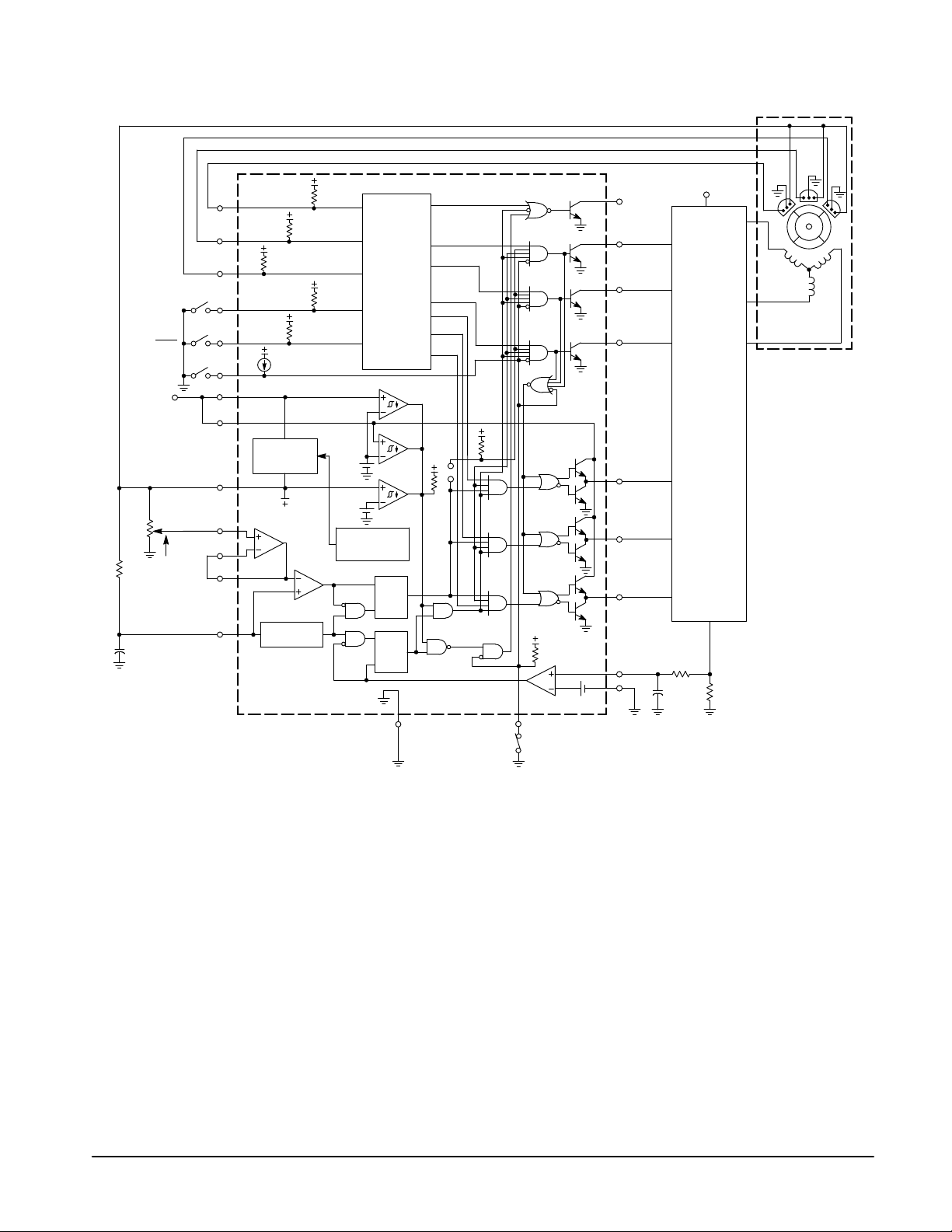
FUNCTIONAL DESCRIPTION
A representative internal block diagram is shown in
Figure 19 with various applications shown in Figures 36, 38,
39, 43, 45, and 46. A discussion of the features and function
of each of the internal blocks given below is referenced to
Figures 19 and 36.
Rotor Position Decoder
An internal rotor position decoder monitors the three
sensor inputs (Pins 4, 5, 6) to provide the proper sequencing
of the top and bottom drive outputs. The sensor inputs are
designed to interface directly with open collector type Hall
Effect switches or opto slotted couplers. Internal pull–up
resistors are included to minimize the required number of
external components. The inputs are TTL compatible, with
their thresholds typically at 2.2 V. The MC33035 series is
designed to control three phase motors and operate with four
of the most common conventions of sensor phasing. A
60°/120
the MC33035 to configure itself to control motors having
either 60°, 120°, 240° or 300° electrical sensor phasing. With
three sensor inputs there are eight possible input code
combinations, six of which are valid rotor positions. The
remaining two codes are invalid and are usually caused by an
open or shorted sensor line. With six valid input codes, the
° Select (Pin 22) is conveniently provided and affords
8
MOTOROLA ANALOG IC DEVICE DATA
Page 9

MC33035
decoder can resolve the motor rotor position to within a
window of 60 electrical degrees.
The Forward/Reverse input (Pin 3) is used to change the
direction of motor rotation by reversing the voltage across the
stator winding. When the input changes state, from high to
low with a given sensor input code (for example 100), the
enabled top and bottom drive outputs with the same alpha
designation are exchanged (AT to AB, BT to BB, CT to CB). In
effect, the commutation sequence is reversed and the motor
changes directional rotation.
Motor on/off control is accomplished by the Output Enable
(Pin 7). When left disconnected, an internal 25 µA current
source enables sequencing of the top and bottom drive
outputs. When grounded, the top drive outputs turn off and
the bottom drives are forced low, causing the motor to coast
and the Fault
output to activate.
Dynamic motor braking allows an additional margin of
safety to be designed into the final product. Braking is
accomplished by placing the Brake Input (Pin 23) in a high
state. This causes the top drive outputs to turn off and the
bottom drives to turn on, shorting the motor–generated back
EMF. The brake input has unconditional priority over all other
inputs. The internal 40 kΩ pull–up resistor simplifies
interfacing with the system safety–switch by insuring brake
activation if opened or disconnected. The commutation logic
truth table is shown in Figure 20. A four input NOR gate is
used to monitor the brake input and the inputs to the three
top drive output transistors. Its purpose is to disable braking
until the top drive outputs attain a high state. This helps to
prevent simultaneous conduction of the the top and bottom
power switches. In half wave motor drive applications, the
top drive outputs are not required and are normally left
disconnected. Under these conditions braking will still be
accomplished since the NOR gate senses the base voltage
to the top drive output transistors.
Error Amplifier
A high performance, fully compensated error amplifier with
access to both inputs and output (Pins 11, 12, 13) is provided
to facilitate the implementation of closed loop motor speed
control. The amplifier features a typical DC voltage gain of
80 dB, 0.6 MHz gain bandwidth, and a wide input common
mode voltage range that extends from ground to V
. In most
ref
open loop speed control applications, the amplifier is
configured as a unity gain voltage follower with the
noninverting input connected to the speed set voltage source.
Additional configurations are shown in Figures 31 through 35.
Oscillator
The frequency of the internal ramp oscillator is
programmed by the values selected for timing components
RT and CT. Capacitor CT is charged from the Reference
Output (Pin 8) through resistor RT and discharged by an
internal discharge transistor. The ramp peak and valley
voltages are typically 4.1 V and 1.5 V respectively . To provide
a good compromise between audible noise and output
switching efficiency, an oscillator frequency in the range of
20 to 30 kHz is recommended. Refer to Figure 1 for
component selection.
Sensor
Inputs
Forward/Reverse
60°/120°Select
Output Enable
V
in
Reference Output
Noninv. Input
Faster
R
T
Error Amp Out
PWM Input
C
T
Sink Only
Positive True
=
Logic With
Hysteresis
Figure 19. Representative Block Diagram
V
14
2
A
1
B
24
C
21
20
19
9
15
20 k
20 k
40 k
25
µ
A
Undervoltage
Lockout
PWM
20 k
40 k
9.1 V
4.5 V
Rotor
Position
Decoder
Thermal
Shutdown
Latch
R
S
Latch
S
R
16
Q
Q
40 k
100 mV
23Gnd
Brake Input
4
S
A
5
S
B
6
S
C
3
22
7
17
V
CC
18
V
C
Reference
Regulator
8
11
Error Amp
12
13
10
Oscillator
M
Fault
Output
T
T
T
A
B
B
B
C
B
Current Sense Input
Current Sense
Reference Input
Top
Drive
Outputs
Bottom
Drive
Outputs
MOTOROLA ANALOG IC DEVICE DATA
9
Page 10

MC33035
Figure 20. Three Phase, Six Step Commutation Truth Table (Note 1)
Inputs (Note 2) Outputs (Note 3)
Sensor Electrical Phasing (Note 4) Top Drives Bottom Drives
60°
S
S
A
1
1
1
0
0
0
1
1
1
0
0
0
1
0
1
0
V V V V V V X 1 1 X 1 1 1 1 1 1 1 (Note 8)
V V V V V V X 0 1 X 1 1 1 1 1 1 0 (Note 9)
V V V V V V X 0 0 X 1 1 1 0 0 0 0 (Note 10)
V V V V V V X 1 0 1 1 1 1 0 0 0 0 (Note 1 1)
NOTES: 1. V = Any one of six valid sensor or drive combinations X = Don’t care.
SCS
B
0
0
1
0
1
1
1
1
0
1
0
0
0
0
1
0
1
1
1
1
0
1
0
0
011
0
011
0
2. The digital inputs (Pins 3, 4, 5, 6, 7, 22, 23) are all TTL compatible. The current sense input (Pin 9) has a 100 mV threshold with respect to Pin 15.
A logic 0 for this input is defined as < 85 mV, and a logic 1 is > 115 mV.
3. The fault and top drive outputs are open collector design and active in the low (0) state.
4. With 60°/120
is for 120° sensor electrical phasing inputs.
5. Valid 60° or 120° sensor combinations for corresponding valid top and bottom drive outputs.
6. Invalid sensor inputs with brake = 0; All top and bottom drives off, Fault
7. Invalid sensor inputs with brake = 1; All top drives off, all bottom drives on, Fault
8. Valid 60° or 120°sensor inputs with brake = 1; All top drives off, all bottom drives on, Fault
9. Valid sensor inputs with brake = 1 and enable = 0; All top drives of f, all bottom drives on, Fault
10. Valid sensor inputs with brake = 0 and enable = 0; All top and bottom drives off, Fault
11. All bottom drives off, Fault
Pulse Width Modulator
The use of pulse width modulation provides an energy
efficient method of controlling the motor speed by varying the
average voltage applied to each stator winding during the
commutation sequence. As CT discharges, the oscillator sets
both latches, allowing conduction of the top and bottom drive
outputs. The PWM comparator resets the upper latch,
terminating the bottom drive output conduction when the
positive–going ramp of CT becomes greater than the error
amplifier output. The pulse width modulator timing diagram is
shown in Figure 21. Pulse width modulation for speed control
appears only at the bottom drive outputs.
Current Limit
Continuous operation of a motor that is severely
over–loaded results in overheating and eventual failure.
This destructive condition can best be prevented with the
use of cycle–by–cycle current limiting. That is, each
on–cycle is treated as a separate event. Cycle–by–cycle
current limiting is accomplished by monitoring the stator
current build–up each time an output switch conducts, and
upon sensing an over current condition, immediately turning
off the switch and holding it off for the remaining duration of
oscillator ramp–up period. The stator current is converted to
a voltage by inserting a ground–referenced sense resistor R
(Figure 36) in series with the three bottom switch transistors
(Q4, Q5, Q6). The voltage developed across the sense
resistor is monitored by the Current Sense Input (Pins 9 and
15), and compared to the internal 100 mV reference. The
current sense comparator inputs have an input common
mode range of approximately 3.0 V. If the 100 mV current
sense threshold is exceeded, the comparator resets the
120°
S
S
low.
C
0
0
0
1
1
1
0
0
0
1
1
1
0
0
F/R Enable
1
1
1
1
1
1
0
0
0
0
0
0
X
X
X
X
B
A
1
0
1
1
0
1
0
1
0
0
1
0
1
0
1
1
0
1
0
1
0
0
1
0
10101
10101
° select (Pin 22) in the high (1) state, configuration is for 60°sensor electrical phasing inputs. With Pin 22 in low (0) state, configuration
Brake
1
1
1
1
1
1
1
1
1
1
1
1
X
X
X
X
Current
Sense
0
0
0
0
0
0
0
0
0
0
0
0
0
0
1
1
0
0
0
0
0
0
0
0
0
0
0
0
X
X
X
X
low.
BTCTABBBCBFault
A
T
0
1
1
0
1
1
1
1
0
1
1
0
0
1
1
111
111
low.
low.
0
0
1
1
1
1
1
1
1
0
0
1
1
high.
low.
1
1
0
0
1
0
0
1
1
1
1
1
1
1
1
0
0
0
1
0
1
0
0
1
0
1
1
0
0
1
0
1
0
0
0
0
1
0
0
000
0
1
111
1
1
1
1
1
0
1
0
1
0
1
0
1
0
1
0
1
0
1
1
1
1
1
0
1
0
0
0
Brake = 0
0
1
0
Brake = 1
lower sense latch and terminates output switch conduction.
The value for the current sense resistor is:
RS+
0.1
I
stator(max)
The Fault output activates during an over current condition.
The dual–latch PWM configuration ensures that only one
single output conduction pulse occurs during any given
oscillator cycle, whether terminated by the output of the error
amp or the current limit comparator.
Figure 21. Pulse Width Modulator Timing Diagram
Capacitor C
Error Amp Out/
Sense Input
S
Bottom Drive
Fault Output
T
PWM Input
Current
Latch “Set”
Inputs
Top Drive
Outputs
Outputs
(Note 5)
F/R = 1
(Note 5)
F/R = 0
(Note 6)
(Note 7)
10
MOTOROLA ANALOG IC DEVICE DATA
Page 11

MC33035
Reference
The on–chip 6.25 V regulator (Pin 8) provides charging
current for the oscillator timing capacitor, a reference for the
error amplifier, and can supply 20 mA of current suitable for
directly powering sensors in low voltage applications. In
higher voltage applications, it may become necessary to
transfer the power dissipated by the regulator off the IC. This
is easily accomplished with the addition of an external pass
transistor as shown in Figure 22. A 6.25 V reference level
was chosen to allow implementation of the simpler NPN
circuit, where V
– VBE exceeds the minimum voltage
ref
required by Hall Effect sensors over temperature. With
proper transistor selection and adequate heatsinking, up to
one amp of load current can be obtained.
Figure 22. Reference Output Buffers
UVLO
UVLO
39
17
18
8
To
Control
Circuitry
6.25 V
17
18
0.1
8
REF
REF
V
in
MPS
U01A
Sensor
Power
≈
5.6 V
V
in
MPS
U51A
To Control Circuitry
and Sensor Power
6.25 V
The NPN circuit is recommended for powering Hall or opto sensors, where the
output voltage temperature coefficient is not critical. The PNP circuit is slightly
more complex, but is also more accurate over temperature. Neither circuit has
current limiting.
Undervoltage Lockout
A triple Undervoltage Lockout has been incorporated to
prevent damage to the IC and the external power switch
transistors. Under low power supply conditions, it guarantees
that the IC and sensors are fully functional, and that there is
sufficient bottom drive output voltage. The positive power
supplies to the IC (VCC) and the bottom drives (VC) are each
monitored by separate comparators that have their
thresholds at 9.1 V. This level ensures sufficient gate drive
necessary to attain low R
when driving standard power
DS(on)
MOSFET devices. When directly powering the Hall sensors
from the reference, improper sensor operation can result if
the reference output voltage falls below 4.5 V. A third
comparator is used to detect this condition. If one or more of
the comparators detects an undervoltage condition, the Fault
Output is activated, the top drives are turned off and the
bottom drive outputs are held in a low state. Each of the
comparators contain hysteresis to prevent oscillations when
crossing their respective thresholds.
Fault
Output
The open collector Fault
Output (Pin 14) was designed to
provide diagnostic information in the event of a system
malfunction. It has a sink current capability of 16 mA and
can directly drive a light emitting diode for visual indication.
Additionally, it is easily interfaced with TTL/CMOS logic for
use in a microprocessor controlled system. The Fault
Output is active low when one or more of the following
conditions occur:
1) Invalid Sensor Input code
2) Output Enable at logic [0]
3) Current Sense Input greater than 100 mV
4) Undervoltage Lockout, activation of one or more of
the comparators
5) Thermal Shutdown, maximum junction temperature
being exceeded
This unique output can also be used to distinguish
between motor start–up or sustained operation in an
overloaded condition. With the addition of an RC network
between the Fault
Output and the enable input, it is possible
to create a time–delayed latched shutdown for overcurrent.
The added circuitry shown in Figure 23 makes easy starting
of motor systems which have high inertial loads by providing
additional starting torque, while still preserving overcurrent
protection. This task is accomplished by setting the current
limit to a higher than nominal value for a predetermined time.
During an excessively long overcurrent condition, capacitor
C
will charge, causing the enable input to cross its
DLY
threshold to a low state. A latch is then formed by the positive
feedback loop from the Fault
Output to the Output Enable.
Once set, by the Current Sense Input, it can only be reset by
shorting C
or cycling the power supplies.
DLY
Drive Outputs
The three top drive outputs (Pins 1, 2, 24) are open
collector NPN transistors capable of sinking 50 mA with a
minimum breakdown of 30 V. Interfacing into higher voltage
applications is easily accomplished with the circuits shown in
Figures 24 and 25.
The three totem pole bottom drive outputs (Pins 19, 20,
21) are particularly suited for direct drive of N–Channel
MOSFETs or NPN bipolar transistors (Figures 26, 27, 28
and 29). Each output is capable of sourcing and sinking up
to 100 mA. Power for the bottom drives is supplied from V
(Pin 18). This separate supply input allows the designer
added flexibility in tailoring the drive voltage, independent of
VCC. A zener clamp should be connected to this input when
driving power MOSFETs in systems where VCC is greater
than 20 V so as to prevent rupture of the MOSFET gates.
The control circuitry ground (Pin 16) and current sense
inverting input (Pin 15) must return on separate paths to the
central input source ground.
Thermal Shutdown
Internal thermal shutdown circuitry is provided to protect
the IC in the event the maximum junction temperature is
exceeded. When activated, typically at 170°C, the IC acts
as though the Output Enable was grounded.
C
MOTOROLA ANALOG IC DEVICE DATA
11
Page 12

MC33035
R
DLY
V
M
Reset
C
DLY
Figure 23. Timed Delayed Latched
Over Current Shutdown
4
5
22
17
18
6
3
REF
8
25
7
POS
DEC
UVLO
µ
A
14
2
1
24
21
20
Figure 24. High V oltage Interface with
NPN Power Transistors
14
2
Rotor
Position
Decoder
1
24
21
20
19
V
M
V
CC
Q
2
Q
Q
1
3
Load
Q
4
V
–(IILenable R
t
DLY
[
[
R
R
DLYCDLY
DLYCDLY
In
In
ref
ǒ
Vthenable – (IILenable R
6.25 – (20 x 10–6R
ǒ
1.4–(20x10–6R
Figure 25. High Voltage Interface with
N–Channel Power MOSFETs
Rotor
Position
Decoder
14
VCC = 12
2
1
24
21
DLY
DLY
1.0 k
1
2
1.0 M
4.7 k
MOC8204
Optocoupler
DLY
)
V
)
DLY
)
Ǔ
V
Boost
5
6
4
1N4744
Ǔ
)
VM =
Load
170 V
Transistor Q1 is a common base stage used to level shift from VCC to the
high motor voltage, VM. The collector diode is required if VCC is present
while VM is low.
Figure 26. Current Waveform Spike Suppression
21
20
19
23
40 k
100 mV
9
15
Brake Input
R
C
R
S
12
20
19
The addition of the RC filter will eliminate current–limit instability caused by the
Q
4
leading edge spike on the current waveform. Resistor RS should be a low
inductance type.
MOTOROLA ANALOG IC DEVICE DATA
Page 13

MC33035
Figure 27. MOSFET Drive Precautions Figure 28. Bipolar Transistor Drive
21
R
g
C
21
D
20
R
g
20
C
D
19
R
g
C
19
D
23
40 k
100 mV
9
15
Brake Input
40 k
100 mV
23
Series gate resistor Rg will dampen any high frequency oscillations caused
by the MOSFET input capacitance and any series wiring induction in the
gate–source circuit. Diode D is required if the negative current into the Bottom Drive Outputs exceeds 50 mA.
9
15
Brake Input
D = 1N5819
The totem–pole output can furnish negative base current for enhanced transistor turn–off, with the addition of capacitor C.
Figure 29. Current Sensing Power MOSFETs Figure 30. High Voltage Boost Supply
I
B
+
0
–
t
Base Charge
Removal
D
SENSEFET
21
S
G
K
M
20
19
9
R
15
S
100 mV
16 Gnd
Control Circuitry Ground (Pin 16) and Current Sense Inverting Input (Pin 15)
must return on separate paths to the Central Input Source Ground.
Virtually lossless current sensing can be achieved with the implementation of
SENSEFET power switches.
Power Ground:
To Input Source Return
RS@
Ipk@
R
V
[
9
Pin
r
DM(on)
DS(on)
)
R
S
If: SENSEFET = MPT10N10M
Ω
Pin 9
, 1/4 W
≈
0.75 I
pk
RS = 200
Then : V
VCC = 12 V
8
6
5
2
1
MC1555
0.001
This circuit generates V
R
S
18 k
VM + 12
VM + 8.0
4
Q
7
3
* = MUR115
Boost
BoostVoltage (V)
VM + 4.0
1.0/200 V
1N5352A
for Figure 25.
0
Boost Current (mA)
20
40
*
22
*
VM = 170 V
V
Boost
60
MOTOROLA ANALOG IC DEVICE DATA
13
Page 14

MC33035
Figure 31. Differential Input Speed Controller
REF
8
7
R
1
V
A
V
B
V
13
Pin
11
R
2
R
3
12
13
R
4
R3)
+
V
ǒ
A
)
R
1
25 µA
EA
PWM
R
R
4
Ǔ
R
2
R
2
4
*
V
ǒ
Ǔ
R
3
B
R
3
Figure 33. Digital Speed Controller Figure 34. Closed Loop Speed Control
5.0 V
BCD
Inputs
12
13
14
15
16
V
P3
P2
P1
P0
Gnd
8
11
Q
CC
9
10
Q
8
9
Q
7
7
Q
6
6
Q
5
5
Q
4
SN74LS145
4
Q
3
3
Q
2
2
Q
1
1
Q
0
166 k
145 k
126 k
108 k
92.3 k
77.6 k
63.6 k
51.3 k
40.4 k
100 k
8
7
11
12
13
REF
EA
25
µ
A
PWM
Figure 32. Controlled Acceleration/Deceleration
REF
8
Enable
R
1
Increase
Speed
Resistor R1 with capacitor C sets the acceleration time constant while R
controls the deceleration. The values of R1 and R2 should be at least ten
times greater than the speed set potentiometer to minimize time constant
variations with different speed settings.
To Sensor
Input (Pin 4)
0.01
10 k
0.1
R
10 k
100 k
1.0 M
2
C
0.22
7
11
12
13
8
7
11
12
13
1.0 M
25 µA
EA
PWM
REF
25 µA
EA
PWM
2
The SN74LS145 is an open collector BCD to One of T en decoder . When connected as shown, input codes 0000 through 1001 steps the PWM in
increments of approximately 10% from 0 to 90% on–time. Input codes 1010
through 1111 will produce 100% on–time or full motor speed.
Figure 35. Closed Loop T emperature Control
R3)
R
V
+
V
ǒ
3
Pi
V
B
R3§§
This circuit can control the speed of a cooling fan proportional to the difference
between the sensor and set temperatures. The control loop is closed as the
forced air cools the NTC thermistor. For controlled heating applications,
exchange the positions of R1 and R2.
ref
n
V
ref
+
R
5
)
ǒ
R
6
R5ø
4
Ǔ
)
R
R
2
1
1
Ǔ
R
5
R
6
R
6
14
The rotor position sensors can be used as a tachometer. By dif ferentiating
the positive–going edges and then integrating them over time, a voltage
proportional to speed can be generated. The error amp compares this
voltage to that of the speed set to control the PWM.
R
R
2
4
*
V
ǒ
Ǔ
R
3
R
1
R
3
B
R
3
8
7
T
11
R
2
12
R
13
4
REF
25 µA
EA
PWM
MOTOROLA ANALOG IC DEVICE DATA
Page 15

MC33035
SYSTEM APPLICATIONS
Three Phase Motor Commutation
The three phase application shown in Figure 36 is a
full–featured open loop motor controller with full wave, six
step drive. The upper power switch transistors are
Darlingtons while the lower devices are power MOSFETs.
Each of these devices contains an internal parasitic catch
diode that is used to return the stator inductive energy back to
the power supply. The outputs are capable of driving a delta
or wye connected stator, and a grounded neutral wye if split
supplies are used. At any given rotor position, only one top
and one bottom power switch (of different totem poles) is
enabled. This configuration switches both ends of the stator
winding from supply to ground which causes the current flow
to be bidirectional or full wave. A leading edge spike is usually
present on the current waveform and can cause a
current–limit instability. The spike can be eliminated by
adding an RC filter in series with the Current Sense Input.
Using a low inductance type resistor for RS will also aid in
spike reduction. Care must be taken in the selection of the
Figure 36. Three Phase, Six Step, Full Wave Motor Controller
4
bottom power switch transistors so that the current during
braking does not exceed the device rating. During braking,
the peak current generated is limited only by the series
resistance of the conducting bottom switch and winding.
I
peak
+
R
switch
VM)
)
EMF
R
winding
If the motor is running at maximum speed with no load, the
generated back EMF can be as high as the supply voltage,
and at the onset of braking, the peak current may approach
twice the motor stall current. Figure 37 shows the
commutation waveforms over two electrical cycles. The first
cycle (0° to 360°) depicts motor operation at full speed while
the second cycle (360° to 720°) shows a reduced speed with
about 50% pulse width modulation. The current waveforms
reflect a constant torque load and are shown synchronous to
the commutation frequency for clarity .
V
M
14
Fault
Ind.
Fwd/Rev
60°/120
Enable
V
R
T
C
T
°
M
Speed
Set
Faster
5
6
3
22
7
17
18
8
11
12
13
10
25
Reference
Regulator
Error Amp
Oscillator
µ
A
Undervoltage
Lockout
PWM
Rotor
Position
Decoder
Thermal
Shutdown
R
S
S
R
2
1
24
21
20
Q
Q
I
Limit
19
9
15
Q
3
Q
6
C
Q
1
Q
2
Q
4
Q
5
R
R
S
N
S
A
B
C
S
N
Motor
MOTOROLA ANALOG IC DEVICE DATA
Gnd 16
23
Brake
15
Page 16

MC33035
Figure 37. Three Phase, Six Step, Full Wave Commutation W aveforms
Rotor Electrical Position (Degrees)
Sensor Inputs
60°/120
Select Pin
Open
Sensor Inputs
60°/120
Select Pin
Grounded
Top Drive
Outputs
480420360300240180120600
S
A
S
B
°
S
C
Code
S
°
Code
100
A
S
B
S
C
100 110 001011 001011110100010 010 101101
A
T
B
T
100
000001011111110
011111110
720660600540
000001
Bottom Drive
Outputs
Conducting
Power Switch
Transistors
Motor Drive
Current
C
T
A
B
B
B
C
B
6
Q2 + Q
Q1 + Q
+
O
A
–
+
O
B
–
+
O
C
–
Q2 + Q4Q3 + Q4Q3 + Q5Q1 + Q5Q1 + Q
6
Fwd/Rev = 1
Q2 + Q6Q2 + Q4Q3 + Q4Q3 + Q
6
Reduced Speed ( ≈ 50% PWM)Full Speed (No PWM)
5
Q1 + Q
5
16
MOTOROLA ANALOG IC DEVICE DATA
Page 17

MC33035
Figure 38 shows a three phase, three step, half wave motor
controller. This configuration is ideally suited for automotive
and other low voltage applications since there is only one
power switch voltage drop in series with a given stator
winding. Current flow is unidirectional or half wave because
only one end of each winding is switched. Continuous braking
with the typical half wave arrangement presents a motor
overheating problem since stator current is limited only by the
winding resistance. This is due to the lack of upper power
switch transistors, as in the full wave circuit, used to
disconnect the windings from the supply voltage VM. A unique
Figure 38. Three Phase, Three Step, Half Wave Motor Controller
4
5
Rotor
Position
Decoder
Fwd/Rev
6
3
solution is to provide braking until the motor stops and then
turn off the bottom drives. This can be accomplished by using
the Fault
over current timer. Components R
Output in conjunction with the Output Enable as an
DL Y
and C
are selected
DL Y
to give the motor sufficient time to stop before latching the
Output Enable and the top drive AND gates low. When
enabling the motor, the brake switch is closed and the PNP
transistor (along with resistors R1 and R
the latch by discharging C
. The stator flyback voltage is
DLY
) are used to reset
DL Y
clamped by a single zener and three diodes.
Motor
C
DLY
14
2
1
R
DLY
R
2
R
1
N
SS
V
M
N
R
T
C
60°/120
V
T
°
M
Speed
Set
Faster
22
7
17
18
8
11
12
13
10
25
µ
Reference
Regulator
Error Amp
Oscillator
A
Undervoltage
Lockout
PWM
Thermal
Shutdown
R
S
S
R
24
21
20
Q
Q
I
Limit
19
9
15
MOTOROLA ANALOG IC DEVICE DATA
Gnd
16
23
Brake
17
Page 18

MC33035
Three Phase Closed Loop Controller
The MC33035, by itself, is only capable of open loop
motor speed control. For closed loop motor speed control,
the MC33035 requires an input voltage proportional to the
motor speed. Traditionally, this has been accomplished by
means of a tachometer to generate the motor speed
feedback voltage. Figure 39 shows an application whereby
an MC33039, powered from the 6.25 V reference (Pin 8) of
the MC33035, is used to generate the required feedback
voltage without the need of a costly tachometer. The same
Hall sensor signals used by the MC33035 for rotor position
decoding are utilized by the MC33039. Every positive or
negative going transition of the Hall sensor signals on any of
the sensor lines causes the MC33039 to produce an output
pulse of defined amplitude and time duration, as determined
by the external resistor R1 and capacitor C1. The output train
Figure 39. Closed Loop Brushless DC Motor Control
Using The MC33035 and MC33039
of pulses at Pin 5 of the MC33039 are integrated by the error
amplifier of the MC33035 configured as an integrator to
produce a DC voltage level which is proportional to the
motor speed. This speed proportional voltage establishes
the PWM reference level at Pin 13 of the MC33035 motor
controller and closes the feedback loop. The MC33035
outputs drive a TMOS power MOSFET 3–phase bridge.
High currents can be expected during conditions of start–up,
breaking, and change of direction of the motor.
The system shown in Figure 39 is designed for a motor
having 120/240 degrees Hall sensor electrical phasing. The
system can easily be modified to accommodate 60/300
degree Hall sensor electrical phasing by removing the
jumper (J2) at Pin 22 of the MC33035.
Enable
Speed
10 k
Faster
100 k
F/R
4.7 k
5.1 k
0.01
1
2
3
4
1
2
3
4
5
6
7
8
9
10
11
12
MC33039
MC33035
1.0 M
0.1
Close Loop
8
7
6
5
1.0 k
1.0 k
24
23
22
21
20
19
18
17
16
15
14
13
J
2
J
1
1.0 M
R
750 pF
C
TP
1
1
1
1.0 k
Brake
1N5819
1N5355B
18 V
VM (18 to 30 V)
1.1 k 1.1 k
470
470
470
330
0.1
1N4148
2.2 k
Latch On
Fault
1.1 k
2.2 k
Fault
0.1
Reset
47 µF
0.1
1000
100
33
TP
2
0.05/1.0 W
S
Motor
N
S
N
18
MOTOROLA ANALOG IC DEVICE DATA
Page 19

MC33035
Sensor Phasing Comparison
There are four conventions used to establish the relative
phasing of the sensor signals in three phase motors. With six
step drive, an input signal change must occur every 60
electrical degrees; however, the relative signal phasing is
dependent upon the mechanical sensor placement. A
comparison of the conventions in electrical degrees is shown
in Figure 40. From the sensor phasing table in Figure 41,
note that the order of input codes for 60° phasing is the
reverse of 300°. This means the MC33035, when configured
for 60° sensor electrical phasing, will operate a motor with
either 60° or 300° sensor electrical phasing, but resulting in
opposite directions of rotation. The same is true for the part
when it is configured for 120° sensor electrical phasing; the
motor will operate equally, but will result in opposite
directions of rotation for 120° for 240° conventions.
Figure 40. Sensor Phasing Comparison
Rotor Electrical Position (Degrees)
720660600540480420360300240180120600
S
A
60°
S
B
S
C
S
A
120°
S
B
S
C
S
A
S
240°
Sensor Electrical Phasing
300°
SASBSCSASBSCSASBSCSASBS
1 0 0 1 0 1 1 1 0 1 1 1
1 1 0 1 0 0 1 0 0 1 1 0
1 1 1 1 1 0 1 0 1 1 0 0
0 1 1 0 1 0 0 0 1 0 0 0
0 0 1 0 1 1 0 1 1 0 0 1
0 0 0 0 0 1 0 1 0 0 1 1
B
S
C
S
A
S
B
S
C
Figure 41. Sensor Phasing T able
Sensor Electrical Phasing (Degrees)
60° 120° 240° 300°
C
In this data sheet, the rotor position is always given in
electrical degrees since the mechanical position is a function
of the number of rotating magnetic poles. The relationship
between the electrical and mechanical position is:
Electrical Degrees+Mechanical Degrees
ǒ
Ǔ
2
#Rotor Poles
An increase in the number of magnetic poles causes more
electrical revolutions for a given mechanical revolution.
General purpose three phase motors typically contain a four
pole rotor which yields two electrical revolutions for one
mechanical.
Two and Four Phase Motor Commutation
The MC33035 is also capable of providing a four step
output that can be used to drive two or four phase motors.
The truth table in Figure 42 shows that by connecting sensor
inputs SB and SC together, it is possible to truncate the
number of drive output states from six to four. The output
power switches are connected to BT, CT, BB, and CB.
Figure 43 shows a four phase, four step, full wave motor
control application. Power switch transistors Q1 through Q
are Darlington type, each with an internal parasitic catch
diode. With four step drive, only two rotor position sensors
spaced at 90 electrical degrees are required. The
commutation waveforms are shown in Figure 44.
Figure 45 shows a four phase, four step, half wave motor
controller. It has the same features as the circuit in Figure 38,
except for the deletion of speed control and braking.
Figure 42. T wo and Four Phase, Four Step,
Commutation Truth Table
MC33035 (60°/120° Select Pin Open)
Inputs Outputs
Sensor Electrical
Spacing* = 90°
S
A
1
1
0
0
1
1
0
0
*With MC33035 sensor input SB connected to SC.
S
B
0
1
1
0
0
1
1
0
F/R B
Top Drives Bottom Drives
C
T
1
1
1
1
0
0
0
0
1
0
1
1
1
1
1
0
T
1
1
0
1
0
1
1
1
B
C
B
0
0
0
1
0
1
0
0
B
1
0
0
0
0
0
1
0
8
MOTOROLA ANALOG IC DEVICE DATA
19
Page 20

MC33035
1
Q
S
N
N
S
A
B
C
Motor
D
5
Q
M
V
Ind.
Fault
14
2
Q
3
Q
4
Q
6
Q
S
7
Q
8
Q
R
R
C
Limit
I
9
15
2
1
24
21
20
19
23
Figure 43. Four Phase, Four Step, Full Wave Motor Controller
4
20
Rotor
Position
Decoder
Thermal
Shutdown
Q
S
R
Q
R
S
Gnd 16
Lockout
Undervoltage
Error Amp
11
12
PWM
13
Oscillator
10
T
R
T
C
µ
25 A
22
7
Enable
17
18
M
V
3
5
6
Fwd/Rev
Regulator
Reference
8
MOTOROLA ANALOG IC DEVICE DATA
Page 21

Sensor Inputs
60°/120
Select Pin
Open
Top Drive
Outputs
Bottom Drive
Outputs
Conducting
Power Switch
Transistors
MC33035
Figure 44. Four Phase, Four Step, Full Wave Motor Controller
Rotor Electrical Position (Degrees)
180 270 360 450 540 630 720090
S
A
°
S
B
Code
B
T
C
B
B
C
T
B
Q3 + Q
Q4 + Q
5
Q1 + Q
6
Q2 + Q
7
Q3 + Q
8
Q4 + Q
5
Q1 + Q
6
0001111000011010
Q2 + Q
7
8
Motor Drive
Current
+
A
O
–
+
B
O
–
+
C
O
–
+
D
O
–
Full Speed (No PWM)
Fwd/Rev = 1
MOTOROLA ANALOG IC DEVICE DATA
21
Page 22

M
V
Fault
Ind.
MC33035
N
S
S
N
Motor
S
R
R
C
14
Figure 45. Four Phase, Four Step, Half Wave Motor Controller
4
24
Rotor
Position
1
Decoder
2
21
20
Thermal
Shutdown
19
Q
S
R
9
15
Limit
I
23
Brake
Q
R
S
Gnd 16
Lockout
Undervoltage
Error Amp
11
12
PWM
13
Oscillator
10
µ
25 A
22
7
17
18
3
5
6
Regulator
Reference
8
22
Fwd/Rev
V
Enable
M
T
R
T
C
MOTOROLA ANALOG IC DEVICE DATA
Page 23

MC33035
Brush Motor Control
Though the MC33035 was designed to control brushless
DC motors, it may also be used to control DC brush type
motors. Figure 46 shows an application of the MC33035
driving a MOSFET H–bridge affording minimal parts count to
operate a brush–type motor. Key to the operation is the input
sensor code [100] which produces a top–left (Q1) and a
bottom–right (Q3) drive when the controller’s forward/reverse
pin is at logic [1]; top–right (Q4), bottom–left (Q2) drive is
realized when the Forward/Reverse pin is at logic [0]. This
code supports the requirements necessary for H–bridge
drive accomplishing both direction and speed control.
The controller functions in a normal manner with a pulse
width modulated frequency of approximately 25 kHz. Motor
speed is controlled by adjusting the voltage presented to the
noninverting input of the error amplifier establishing the
PWM’s slice or reference level. Cycle–by–cycle current
limiting of the motor current is accomplished by sensing the
voltage (100 mV) across the RS resistor to ground of the
H–bridge motor current. The over current sense circuit makes
it possible to reverse the direction of the motor, using the
Figure 46. H–Bridge Brush–Type Controller
4
5
Rotor
Position
Decoder
Fwd/Rev
6
3
normal forward/reverse switch, on the fly and not have to
completely stop before reversing.
LAYOUT CONSIDERA TIONS
Do not attempt to construct any of the brushless
motor control circuits on wire–wrap or plug–in prototype
boards. High frequency printed circuit layout techniques are
imperative to prevent pulse jitter. This is usually caused by
excessive noise pick–up imposed on the current sense or
error amp inputs. The printed circuit layout should contain a
ground plane with low current signal and high drive and
output buffer grounds returning on separate paths back to the
power supply input filter capacitor VM. Ceramic bypass
capacitors (0.1 µF) connected
close to the integrated circuit at VCC, VC, V
amp noninverting input may be required depending upon
circuit layout. This provides a low impedance path for filtering
any high frequency noise. All high current loops should be
kept as short as possible using heavy copper runs to
minimize radiated EMI.
Fault
14
2
1
Ind.
20 k
1.0 k
and the error
ref
1.0 k
Q1*
+12 V
10 k
10 k
0.005
Enable
+12 V
Faster
22
7
17
18
8
11
12
13
10
µ
A
25
Reference
Regulator
Error Amp
Oscillator
Undervoltage
Lockout
PWM
Thermal
Shutdown
R
S
S
R
Gnd
24
DC Brush
Motor
21
22
20
9
15
19
1.0 k
0.001
Q
Q
16
I
23
Brake
Limit
M
Q2*
22
Q4*
Q3*
R
S
MOTOROLA ANALOG IC DEVICE DATA
23
Page 24

MC33035
OUTLINE DIMENSIONS
OUTLINE DIMENSIONS
-A-
1324
112
-B-
-T-
SEATING
PLANE
E
G
F
D
N
24 PL
0.25 (0.010) T A
-A-
24 13
-B-
112
D 24 PL
0.010 (0.25) A B
M
S S
T
C
-T-
SEATING
PLANE
G 22 PL
PLASTIC PACKAGE
C
K
M M
PLASTIC PACKAGE
P 12 PL
0.010 (0.25)
J
K
P SUFFIX
CASE 724–03
ISSUE D
L
J 24 PL
0.25 (0.010) T B
DW SUFFIX
CASE 751E–04
(SO–24L)
ISSUE E
M M
B
F
M
NOTE 1
M
M M
R X 45°
NOTES:
1. CHAMFERED CONTOUR OPTIONAL.
2. DIMENSION L TO CENTER OF LEADS WHEN
FORMED PARALLEL.
3. DIMENSIONING AND TOLERANCING PER ANSI
Y14.5M, 1982.
4. CONTROLLING DIMENSION: INCH.
INCHES MILLIMETERS
MIN MINMAX MAX
DIM
A
1.230
B
0.250
C
0.145
D
0.015
E
0.050 BSC
F
0.040
0.100 BSC
G
J
0.007
K
0.110
0.300 BSC
L
M
0
°
N
0.020
NOTES:
1. DIMENSIONING AND TOLERANCING PER ANSI
Y14.5M, 1982.
2. CONTROLLING DIMENSION: MILLIMETER.
3. DIMENSIONS A AND B DO NOT INCLUDE
MOLD PROTRUSION.
4. MAXIMUM MOLD PROTRUSION 0.15 (0.006)
PER SIDE.
5. DIMENSION D DOES NOT INCLUDE DAMBAR
PROTRUSION. ALLOWABLE DAMBAR
PROTRUSION SHALL BE 0.13 (0.005) TOTAL IN
EXCESS OF D DIMENSION AT MAXIMUM
MATERIAL CONDITION.
MILLIMETERS INCHES
MIN MINMAX MAX
DIM
15.25
A
7.40
B
2.35
C
0.35
D
0.41
F
1.27 BSC 0.050 BSC
G
J
0.23
K
0.13
M
0
°
P
10.05
R
0.25
1.265
0.270
0.175
0.020
0.060
0.012
0.140
15
0.040
15.54
7.60
2.65
0.49
0.90
0.32
0.29
8
10.55
0.75
31.25
32.13
6.35
6.85
3.69
4.44
0.38
0.51
1.27 BSC
1.02
1.52
2.54 BSC
0.18
0.30
2.80
3.55
7.62 BSC
0
0.51
0.601
0.292
0.093
0.014
0.016
0.009
0.005
0
°
0.395
0.010
15
°
°
1.01
0.612
0.299
0.104
0.019
0.035
0.013
0.011
8
°
0.415
0.029
°
°
Motorola reserves the right to make changes without further notice to any products herein. Motorola makes no warranty , representation or guarantee regarding
the suitability of its products for any particular purpose, nor does Motorola assume any liability arising out of the application or use of any product or circuit, and
specifically disclaims any and all liability, including without limitation consequential or incidental damages. “T ypical” parameters which may be provided in Motorola
data sheets and/or specifications can and do vary in different applications and actual performance may vary over time. All operating parameters, including “Typicals”
must be validated for each customer application by customer’s technical experts. Motorola does not convey any license under its patent rights nor the rights of
others. Motorola products are not designed, intended, or authorized for use as components in systems intended for surgical implant into the body, or other
applications intended to support or sustain life, or for any other application in which the failure of the Motorola product could create a situation where personal injury
or death may occur. Should Buyer purchase or use Motorola products for any such unintended or unauthorized application, Buyer shall indemnify and hold Motorola
and its officers, employees, subsidiaries, affiliates, and distributors harmless against all claims, costs, damages, and expenses, and reasonable attorney fees
arising out of, directly or indirectly, any claim of personal injury or death associated with such unintended or unauthorized use, even if such claim alleges that
Motorola was negligent regarding the design or manufacture of the part. Motorola and are registered trademarks of Motorola, Inc. Motorola, Inc. is an Equal
Opportunity/Affirmative Action Employer.
Mfax is a trademark of Motorola, Inc.
How to reach us:
USA/EUROPE/Locations Not Listed: Motorola Literature Distribution; JAPAN: Motorola Japan Ltd.; SPD, Strategic Planning Office, 141,
P.O. Box 5405, Denver, Colorado 80217. 1–303–675–2140 or 1–800–441–2447 4–32–1 Nishi–Gotanda, Shinagawa–ku, Tokyo, Japan. 81–3–5487–8488
Customer Focus Center: 1–800–521–6274
Mfax: RMFAX0@email.sps.mot.com – TOUCHTONE 1–602–244–6609 ASIA/P ACIFIC: Motorola Semiconductors H.K. Ltd.; 8B Tai Ping Industrial Park,
Moto rola Fax Ba ck System – US & Canada ONLY 1–800–774–1848 51 Ting Kok Road, Tai Po, N.T., Hong Kong. 852–26629298
– http://sps.motorola.com/mfax/
HOME PAGE: http://motorola.com/sps/
24
◊
MOTOROLA ANALOG IC DEVICE DATA
MC33035/D
 Loading...