

Page 1
查询MC33030供应商
Order this document by MC33030/D
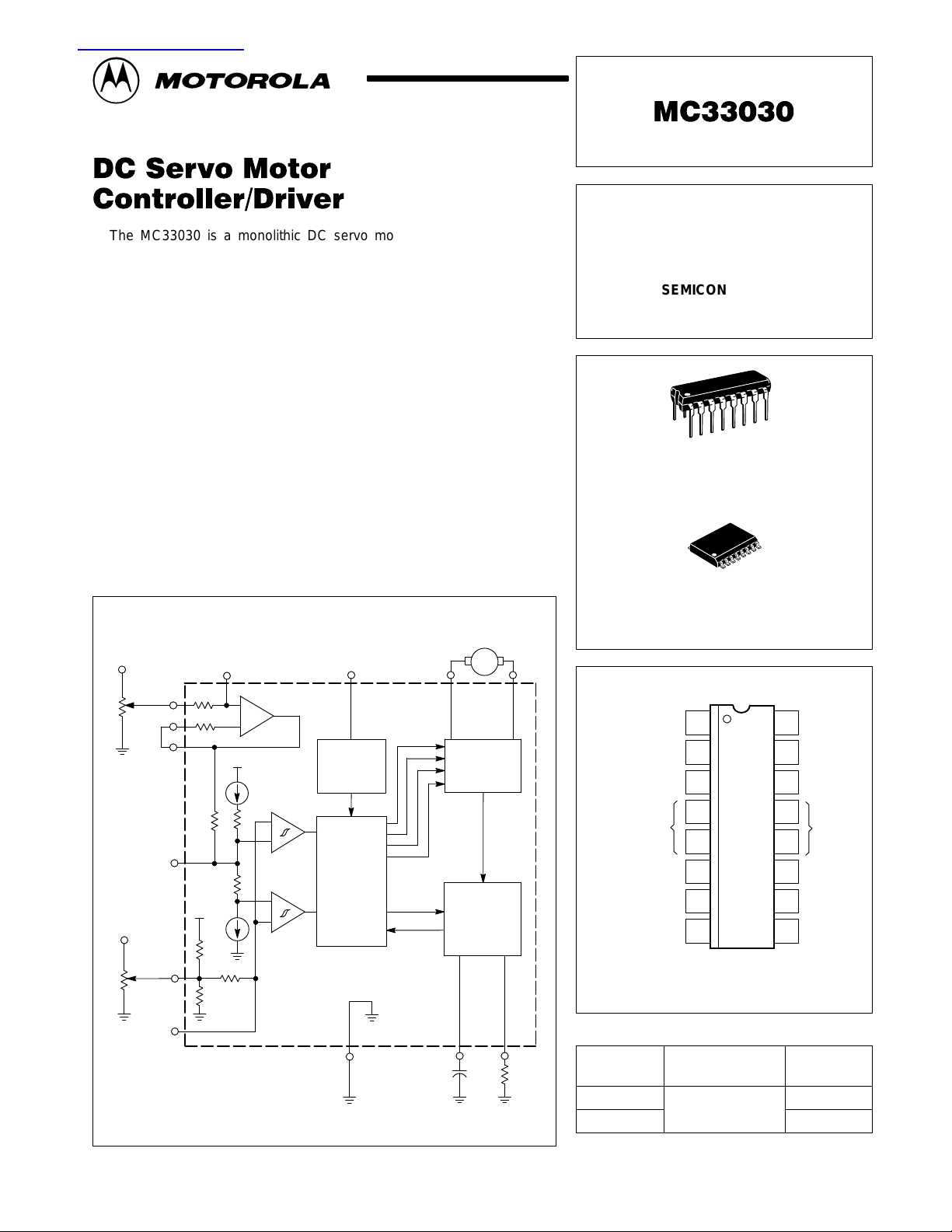
The MC33030 is a monolithic DC servo motor controller providing all
active functions necessary for a complete closed loop system. This device
consists of an on–chip op amp and window comparator with wide input
common–mode range, drive and brake logic with direction memory, Power
H–Switch driver capable of 1.0 A, independently programmable over–current
monitor and shutdown delay, and over–voltage monitor. This part is ideally
suited for almost any servo positioning application that requires sensing of
temperature, pressure, light, magnetic flux, or any other means that can be
converted to a voltage.
Although this device is primarily intended for servo applications, it can be
used as a switchmode motor controller.
• On–Chip Error Amp for Feedback Monitoring
• Window Detector with Deadband and Self Centering Reference Input
• Drive/Brake Logic with Direction Memory
• 1.0 A Power H–Switch
• Programmable Over–Current Detector
• Programmable Over–Current Shutdown Delay
• Over–Voltage Shutdown
Representative Block Diagram
Motor
V
CC
Feedback
Position
V
CC
Reference
Position
9
8
7
6
3
+
1
2
Error Amp
+
–
+
+
–
Window
Detector
+
–
This device contains 119 active transistors.
V
CC
Over–
Voltage
Monitor
Drive/
Brake
Logic
Direction
Memory
4, 5, 12, 13
1011
Programmable
C
DLY
Power
H–Switch
Over–
Current
Detector
& Latch
14
1516
R
OC
DC SERVO MOTOR
CONTROLLER/DRIVER
SEMICONDUCTOR
TECHNICAL DATA
16
1
P SUFFIX
PLASTIC PACKAGE
CASE 648C
(DIP–16)
16
1
DW SUFFIX
PLASTIC PACKAGE
CASE 751G
(SOP–16L)
PIN CONNECTIONS
Reference
Reference
Input Filter
Error Amp Output
Filter/Feedback Input
Gnd
Error Amp
Error Amp
Inverting Input
Error Amp Non–
Inverting Input
Pins 4, 5, 12 and 13 are electrical ground and heat
sink pins for IC.
116
Input
2
3
4
5
6
Output
7
8
(Top View)
ORDERING INFORMATION
Operating
Device
MC33030DW
MC33030P
Temperature Range
TA = –40° to +85°C
Over–Current
Delay
Over–Current
15
Reference
Driver
14
Output A
13
Gnd
12
11
V
CC
Driver
10
Output B
Error Amp
9
Input Filter
Package
SOP–16L
DIP–16
MOTOROLA ANALOG IC DEVICE DATA
Motorola, Inc. 1996 Rev 2
1
Page 2

MC33030
pgg
IR
CC
Ch
Su , ua e Case 6 8C
Th
R
15
(Pins 4, 5, 12, 13)
Thermal Resistance, Junction to Case
R
θJC
18
Input Bias Current (V
Pi
R
L
100 k)
I
IB
7.0
nA
MAXIMUM RATINGS
Rating Symbol Value Unit
Power Supply Voltage V
Input Voltage Range
Op Amp, Comparator, Current Limit
(Pins 1, 2, 3, 6, 7, 8, 9, 15)
Input Differential Voltage Range
Op Amp, Comparator (Pins 1, 2, 3, 6, 7, 8, 9)
Delay Pin Sink Current (Pin 16) I
Output Source Current (Op Amp) I
Drive Output Voltage Range (Note 1) V
Drive Output Source Current (Note 2) I
Drive Output Sink Current (Note 2) I
Brake Diode Forward Current (Note 2) I
Power Dissipation and Thermal
aracteristics
P Suffix, Dual In Line Case 648C
Thermal Resistance, Junction–to–Air
ermal Resistance, Junction–to–Case
(Pins 4, 5, 12, 13)
DW Suffix, Dual In Line Case 751G
Thermal Resistance, Junction–to–Air
Thermal Resistance, Junction–to–Case
(Pins 4, 5, 12, 13)
Operating Junction Temperature T
Operating Ambient Temperature Range T
Storage Temperature Range T
NOTES: 1.The upper voltage level is clamped by the forward drop, VF, of the brake diode.
2. These values are for continuous DC current. Maximum package power dissipation limits must
be observed.
CC
V
IR
V
IDR
DLY(sink)
source
DRV
DRV(source)
DRV(sink)
F
R
θJA
θJC
R
θJA
R
J
A
stg
–0.3 to (VCC + VF) V
36 V
–0.3 to V
–0.3 to V
20 mA
10 mA
1.0 A
1.0 A
1.0 A
80
94
18
+150 °C
–40 to +85 °C
–65 to +150 °C
CC
CC
V
V
°C/W
ELECTRICAL CHARACTERISTICS (V
Characteristic
ERROR AMP
Input Offset Voltage (– 40°C p TA p 85°C)
V
= 7.0 V, RL = 100 k
Pin 6
Input Offset Current (V
Input Common–Mode Voltage Range
∆VIO = 20 mV, RL = 100 k
Slew Rate, Open Loop (VID = 0.5 V, CL = 15 pF) SR – 0.40 – V/µs
Unity–Gain Crossover Frequency f
Unity–Gain Phase Margin φm – 63 – deg.
Common–Mode Rejection Ratio (V
Power Supply Rejection Ratio
VCC = 9.0 to 16 V, V
Output Source Current (V
Output Sink Current (V
Output Voltage Swing (RL = 17 k to Ground) V
NOTES: 3.The upper or lower hysteresis will be lost when operating the Input, Pin 3, close to the respective rail. Refer to Figure 4.
4.Low duty cycle pulse techniques are used during test to maintain junction temperature as close to ambient temperature as possible.
= 1.0 V, RL = 100 k) I
Pin 6
=
6 = 7.0 V,
n
Pin 6
= 7.0 V, RL = 100 k
Pin 6
= 12 V) IO
Pin 6
= 1.0 V) IO
Pin 6
= 14 V, TA = 25°C, unless otherwise noted.)
CC
Symbol Min Typ Max Unit
V
IO
IO
=
=
V
ICR
c
= 7.0 V, RL = 100 k) CMRR 50 82 – dB
PSRR – 89 – dB
+
–
OH
V
OL
– 1.5 10 mV
– 0.7 – nA
–
–
– 0 to (VCC – 1.2) – V
– 550 – kHz
– 1.8 – mA
– 250 – µA
12.5
–
13.1
0.02
–
–
–
–
V
V
2
MOTOROLA ANALOG IC DEVICE DATA
Page 3
MC33030
pg()
pg y
p(IN/DRV)
µ
()
y(
OC DRV
)
DLY(sink)
th(OC)
p(
A
)
()
pg g(
L
p)
()
ELECTRICAL CHARACTERISTICS (continued) (V
Characteristic
WINDOW DETECTOR
Input Hysteresis Voltage (V1 – V4, V2 – V3, Figure 18) V
Input Dead Zone Range (V2 – V4, Figure 18) V
Input OffsetV oltage ([V2 – V
Input Functional Common–Mode Range (Note 3)
Upper Threshold
Lower Threshold V
Reference Input Self Centering Voltage
Pins 1 and 2 Open
Window Detector Propagation Delay
Comparator Input, Pin 3, to Drive Outputs
VID = 0.5 V, R
OVER–CURRENT MONITOR
Over–Current Reference Resistor Voltage (Pin 15) R
Delay Pin Source Current
V
= 0 V, ROC = 27 k, I
DLY
Delay Pin Sink Current (ROC = 27 k, I
V
= 5.0 V
DLY
V
= 8.3 V
DLY
V
= 14 V – 16.5 –
DLY
Delay Pin Voltage, Low State (I
Over–Current Shutdown Threshold
VCC = 14 V
VCC = 8.0 V 5.5 6.0 6.5
Over–Current Shutdown Propagation Delay
Delay Capacitor Input, Pin 16, to Drive Outputs, VID = 0.5 V
L(DRV)
= 390 Ω
] – [V
Pin 2
= 0 mA
DRV
= 0 mA) V
DLY
– V4] Figure 18) V
Pin 2
= 0 mA)
DRV
= 14 V, TA = 25°C, unless otherwise noted.)
CC
Symbol Min Typ Max Unit
H
IDZ
IO
V
IH
IL
V
RSC
t
p(IN/DRV)
OC
I
DLY(source)
I
DLY(sink)
OL(DLY)
V
th(OC)
t
p(DLY/DRV)
25 35 45 mV
166 210 254 mV
– 25 – mV
– (VCC – 1.05)
– 0.24 –
– (1/2 VCC) – V
– 2.0 – µs
3.9 4.3 4.7 V
– 5.5 6.9 µA
– 0.1
– 0.7
– 0.3 0.4 V
6.8
– 1.8 – µs
7.5
–
V
mA
–
–
V
8.2
POWER H–SWITCH
Drive–Output Saturation (– 40°C p TA p+ 85°C, Note 4)
High–State (I
Low–State (I
Drive–Output Voltage Switching T ime (CL = 15 pF)
Rise Time
Fall Time t
Brake Diode Forward Voltage Drop (IF = 200 mA, Note 4) V
TOTAL DEVICE
Standby Supply Current I
Over–Voltage Shutdown Threshold
(– 40°C p TA p + 85°C)
Over–Voltage Shutdown Hysteresis (Device “off” to “on”) V
Operating Voltage Lower Threshold
(– 40°C p TA p + 85°C)
NOTES: 3. The upper or lower hysteresis will be lost when operating the Input, Pin 3, close to the respective rail. Refer to Figure 4.
4.Low duty cycle pulse techniques are used during test to maintain junction temperature as close to ambient temperature as possible.
source
= 100 mA)
sink
= 100 mA)
V
OH(DRV)
V
OL(DRV)
t
r
f
F
CC
V
th(OV)
H(OV)
V
CC
(VCC – 2) (VCC – 0.85)
– 0.12 1.0
– 200
– 200 –
– 1.04 2.5 V
– 14 25 mA
16.5 18 20.5 V
0.3 0.6 1.0 V
– 7.5 8.0 V
–
V
ns
–
MOTOROLA ANALOG IC DEVICE DATA
3
Page 4
MC33030
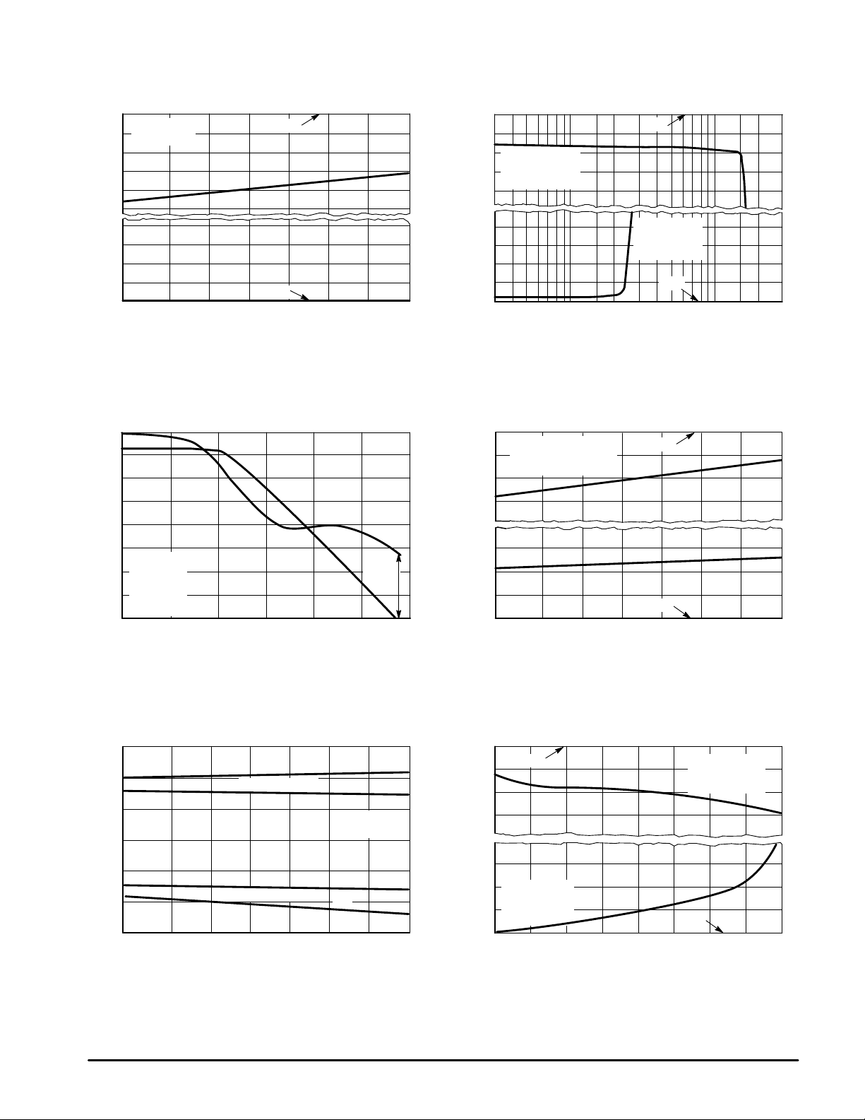
Figure 1. Error Amp Input Common–Mode
V oltage Range versus Temperature
0
∆
VIO = 20 mV
RL = 100 k
– 400
– 800
800
400
, INPUT COMMON–MODE RANGE (mV)
ICR
V
0
– 55
TA, AMBIENT TEMPERATURE (°C)
25 3.0 k100 1.0 k300
Figure 3. Open Loop V oltage Gain and
Phase versus Frequency
80
60
40
VCC = 14
V
= 7.0 V
20
out
RL = 100 k
, OPEN–LOOP VOLTAGE GAIN (dB)
CL = 40 pF
VOL
A
0
1.0 10 100 10 k 100 k 1.0 M1.0 k
TA = 25
°
C
Phase
f, FREQUENCY (Hz)
Gnd
V
CC
Gain
10050 750– 25
Phase
Margin
= 63
Figure 2. Error Amp Output Saturation
versus Load Current
125
0
– 1.0
Source Saturation
RL to Gnd
TA = 25
– 2.0
2.0
1.0
, OUTPUT SA TURATION VOLTAGE (V)
sat
V
0
30
°
C
IL, LOAD CURRENT (
V
CC
Sink Saturation
RL to VCC
°
C
TA = 25
Gnd
± µ
A)
Figure 4. Window Detector Reference–Input
Common–Mode V oltage Range
versus T emperature
0
45
90
135
°
, EXCESS PHASE (DEGREES)
φ
180
0
Max. Pin 2 V
Pin 3 can change
– 0.5
state of drive outputs.
– 1.0
– 1.5
0.3
0.2
, INPUT COMMON–MODE RANGE (V)
0.1
ICR
V
0
– 55
– 25
so that
ICR
0 255075100
TA, AMBIENT TEMPERATURE (
V
CC
Gnd
125
°
C)
Figure 5. Window Detector Feedback–Input
Thresholds versus T emperature
7.15
7.10
7.05
7.00
6.95
, FEEDBACK–INPUT VOLTAGE (V)
6.90
FB
V
6.85
– 55 – 25 125
TA, AMBIENT TEMPERATURE (
Upper Hysteresis
Lower Hysteresis
0 25 50 75 100
V
2
V
3
VCC = 14 V
Pin 2 = 7.00 V
V
1
V
4
°
C)
4
Figure 6. Output Driver Saturation
versus Load Current
0
V
CC
– 1.0
1.0
Sink Saturation
, OUTPUT SA TURATION VOLTAGE (V)
V
RL = VCC
°
C
TA = 25
sat
0
0 200 400 600 800
IL, LOAD CURRENT (±mA)
Source Saturation
RL to Gnd
TA = 25
Gnd
MOTOROLA ANALOG IC DEVICE DATA
°
C
Page 5
MC33030
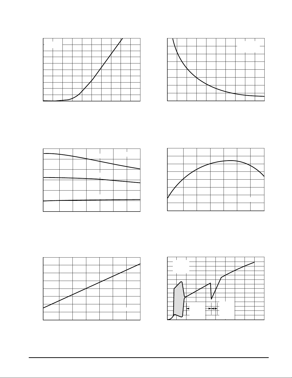
, FORWARD CURRENT (mA)
F
I
500
400
300
200
100
600
400
Figure 7. Brake Diode Forward Current
versus Forward Voltage
TA = 25°C
0
VF, FORWARD VOLTAGE (V)
1.10.90.70.5
Figure 9. Output Source Current–Limit
versus T emperature
ROC = 15 k
ROC = 27 k
1.3
VCC = 14 V
1.5
, OUTPUT SOURCE CURRENT (mA)
source
I
1.04
1.00
0.96
Figure 8. Output Source Current–Limit versus
Over–Current Reference Resistance
800
VCC = 14 V
TA = 25
600
400
200
0
ROC, OVER–CURRENT REFERENCE RESISTANCE (k
Figure 10. Normalized Delay Pin Source
Current versus Temperature
°
C
806040020
100
Ω
)
200
, OUTPUT SOURCE CURRENT (mA)
source
I
0
– 55
TA, AMBIENT TEMPERATURE (°C)
Figure 11. Normalized Over–Current Delay
Threshold V oltage versus Temperature
1.04
1.02
1.00
(NORMALIZED)
0.98
, OVER–CURRENT DELAY THRESHOLD VOLTAGE
0.96
th(OC)
V
0– 25
TA, AMBIENT TEMPERATURE (
ROC = 68 k
25
VCC = 14 V
75 1005025– 55
°
C)
12575500– 25 100
125
(NORMALIZED)
, DELAY PIN SOURCE CURRENT
0.92
DLY(source)
0.88
I
– 55 12525 50 10075
– 25 0
TA, AMBIENT TEMPERATURE (
Figure 12. Supply Current versus
Supply V oltage
28
Pins 6 to 7
Pins 2 to 8
, SUPPLY CURRENT (mA)
CC
I
24
20
16
12
8.0
4.0
0
°
C
TA = 25
Minimum
Operating
Voltage
Range
8.0016
VCC, SUPPLY VOLTAGE (V)
Over–
Voltage
Shutdown
Range
24
VCC = 14 V
°
C)
32 40
MOTOROLA ANALOG IC DEVICE DATA
5
Page 6

MC33030
Figure 13. Normalized Over–Voltage Shutdown
Threshold versus T emperature
1.02
1.00
0.98
(NORMALIZED)
0.96
, OVER–VOLTAGE SHUTDOWN THRESHOLD
– 55 12525 50 100 75
th(OV)
V
– 25 0
TA, AMBIENT TEMPERATURE (°C)
Figure 14. Normalized Over–Voltage Shutdown
1.4
1.2
1.0
0.8
(NORMALIZED)
0.6
, OVER–VOLTAGE SHUTDOWN THRESHOLD
0.4
th(OV)
V
Figure 15. P Suffix (DIP–16) Thermal
Resistance and Maximum Power Dissipation
versus P.C.B. Copper Length
°
100
80
60
R
θ
JA
Printed circuit board heatsink example
2.0 oz
L
Copper
L
Graphs represent symmetrical layout
Hysteresis versus T emperature
– 25 0– 55 125
3.0 mm
25
TA, AMBIENT TEMPERATURE (
5.0
4.0
3.0
75 10050
°
C)
JA
θ
R , THERMAL RESISTANCE
°
JA
JUNCTION–TO–AIR ( C/W)
θ
R , THERMAL RESISTANCE
40
P
for TA = 70°C
20
JUNCTION–TO–AIR ( C/W)
0
0
D(max)
10 20 30 40 50
L, LENGTH OF COPPER (mm)
Figure 16. DW Suffix (SOP–16L) Thermal
Resistance and Maximum Power Dissipation
versus P.C.B. Copper Length
100
P
for TA = 50°C
90
80
70
60
50
40
30
02030504010
R
θ
L, LENGTH OF COPPER (mm)
D(max)
Graph represents symmetrical layout
2.0 oz.
L
Copper
JA
2.0
1.0
, MAXIMUM POWER DISSIPATION (W)
D
P
0
2.8
2.4
2.0
1.6
1.2
3.0 mmL
0.8
0.4
0
, MAXIMUM POWER DISSIPATION (W)
D
P
6
MOTOROLA ANALOG IC DEVICE DATA
Page 7

MC33030
OPERA TING DESCRIPTION
The MC33030 was designed to drive fractional horsepower
DC motors and sense actuator position by voltage feedback. A
typical servo application and representative internal block
diagram are shown in Figure 17. The system operates by
setting a voltage on the reference input of the Window
Dectector (Pin 1) which appears on (Pin 2). A DC motor then
drives a position sensor, usually a potentiometer driven by a
gear box, in a corrective fashion so that a voltage
proportional to position is present at Pin 3. The servo motor
will continue to run until the voltage at Pin 3 falls within the
dead zone, which is centered about the reference voltage.
The Window Detector is composed of two comparators, A
and B, each containing hysteresis. The reference input,
common to both comparators, is pre–biased at 1/2 VCC for
simple two position servo systems and can easily be
overriden by an external voltage divider. The feedback
voltage present at Pin 3 is connected to the center of two
resistors that are driven by an equal magnitude current
source and sink. This generates an offset voltage at the input
of each comparator which is centered about Pin 3 that can
float virtually from VCC to ground. The sum of the upper and
lower offset voltages is defined as the window detector input
dead zone range.
To increase system flexibility, an on–chip Error Amp is
provided. It can be used to buffer and/or gain–up the actuator
position voltage which has the effect of narrowing the dead
zone range. A PNP differential input stage is provided so that
the input common–mode voltage range will include ground.
The main design goal of the error amp output stage was to be
able to drive the window detector input. It typically can source
1.8 mA and sink 250 µA. Special design considerations must
be made if it is to be used for other applications.
The Power H–Switch provides a direct means for motor
drive and braking with a maximum source, sink, and brake
current of 1.0 A continuous. Maximum package power
dissipation limits must be observed. Refer to Figure 15 for
thermal information. For greater drive current requirements,
a method for buffering that maintains all the system features
is shown in Figure 30.
The Over–Current Monitor is designed to distinguish
between motor start–up or locked rotor conditions that can
occur when the actuator has reached its travel limit. A
fraction of the Power H–Switch source current is internally
fed into one of the two inverting inputs of the current
comparator, while the non–inverting input is driven by a
programmable current reference. This reference level is
controlled by the resistance value selected for ROC, and must
be greater than the required motor run–current with its
mechanical load over temperature; refer to Figure 8. During
an over–current condition, the comparator will turn off and
allow the current source to charge the delay capacitor, C
When C
over–current latch will go high, disabling the drive and brake
functions of the Power H–Switch. The programmable time
delay is determined by the capacitance value–selected for
C
DLY
t
DLY
This system allows the Power H–Switch to supply motor
start–up current for a predetermined amount of time. If the
charges to a level of 7.5 V, the set input of the
DLY
.
V
ref
+
I
DLY(source)
C
DLY
+
7.5 C
5.5 µA
DLY
+
1.36 C
DLY
DL Y
in µF
rotor is locked, the system will time–out and shut–down. This
feature eliminates the need for servo end–of–travel or limit
switches. Care must be taken so as not to select too large of
a capacitance value for C
an excessively long time–out period can cause the integrated
circuit to overheat and eventually fail. Again, the maximum
package power dissipation limits must be observed. The
over–current latch is reset upon power–up or by readjusting
V
as to cause V
Pin 2
zone. This can be achieved by requesting the motor to
reverse direction.
An Over–Voltage Monitor circuit provides protection for
the integrated circuit and motor by disabling the Power
H–Switch functions if VCC should exceed 18 V. Resumption
of normal operation will commence when VCC falls below
17.4 V.
A timing diagram that depicts the operation of the
Drive/Brake Logic section is shown in Figure 18. The
waveforms grouped in [1] show a reference voltage that was
preset, appearing on Pin 2, which corresponds to the desired
actuator position. The true actuator position is represented
by the voltage on Pin 3. The points V1 through V4 represent
the input voltage thresholds of comparators A and B that
cause a change in their respective output state. They are
defined as follows:
V1 = Comparator B turn–off threshold
V2 = Comparator A turn–on threshold
V3 = Comparator A turn–off threshold
V4 = Comparator B turn–on threshold
V1–V4 = Comparator B input hysteresis voltage
V2–V3 = Comparator A input hysteresis voltage
V2–V4 = Window detector input dead zone range
|(V2–V
voltage
It must be remembered that points V1 through V4 always
try to follow and center about the reference voltage setting if
it is within the input common–mode voltage range of Pin 3;
Figures 4 and 5. Initially consider that the feedback input
voltage level is somewhere on the dashed line between V
and V4 in [1]. This is within the dead zone range as defined
above and the motor will be off. Now if the reference voltage
is raised so that V
turn–on [3] enabling Q
and B to source motor current [8]. The actuator will move in
Direction B until V
B will turn–off, activating the brake enable [4] and Q
causing Drive Output A to go high and B to go into a high
impedance state. The inertia of the mechanical system will
drive the motor as a generator creating a positive voltage on
.
Pin 10 with respect to Pin 14. The servo system can be
stopped quickly, so as not to over–shoot through the dead
zone range, by braking. This is accomplished by shorting the
motor/generator terminals together. Brake current will flow
into the diode at Drive Output B, through the internal VCC rail,
and out the emitter of the sourcing transistor at Drive Output
A. The end of the solid line and beginning of the dashed for
V
Pin 3
actuator after braking.
) – (V
Pin2
[1] indicates the possible resting position of the
Pin 3
– V4)| = Window detector input
Pin2
Pin 3
Drive, causing Drive Output A to sink
becomes greater than V1. Comparator
Pin 3
. An over–current condition for
DLY
to enter or pass through the dead
is less than V4, comparator B will
2
Brake [6]
MOTOROLA ANALOG IC DEVICE DATA
7
Page 8

MC33030
Figure 17. Representative Block Diagram and T ypical Servo Application
V
CC
Gearbox and Linkage
Motor
V
CC
Inverting
Inverting
Input
Output
Error Amp
Output Filter/
Feedback
Input
V
CC
Reference
Input
Reference
Input Filter
Non–
Input
8
7
6
3
1
2
20 k
20 k
20 k
100 k
100 k
Window
Detector
Input
Filter
9
Error Amp
+
35
µ
A
3.0 k
3.0 k
35
µ
A
+
20 k
0.3 mA
B
A
4, 5,12,13
Gnd
18 V
Ref.
Over–Voltage
Monitor
Drive Brake Logic
Direction
Latch
Brake Enable
Q
Over–
Current
Latch
Q
Drive
Q
Q
R
Q
S
Q Drive
R
S
7.5 V
Ref.
Over–Current
Delay
Q Brake
Brake
Q
5.5
µ
A
50 k
16
C
DLY
11
Drive
Output B
+
R
10
Power
H–Switch
15
Over–Current
Reference
OC
Drive
Output A
14
+
Over–Current
Monitor
If V
should continue to rise and become greater than V2,
Pin 3
the actuator will have over shot the dead zone range and cause
the motor to run in Direction A until V
is equal to V3. The
Pin 3
Drive/Brake behavior for Direction A is identical to that of B.
Overshooting the dead zone range in both directions can cause
the servo system to continuously hunt or oscillate. Notice that the
last motor run–direction is stored in the direction latch. This
information is needed to determine whether Q or Q
enabled when V
enters the dead zone range. The dashed
Pin 3
Brake is to be
lines in [8,9] indicate the resulting waveforms of an over–current
condition that has exceeded the programmed time delay. Notice
that both Drive Outputs go into a high impedance state until V
is readjusted so that V
2
enters or crosses through the dead
Pin 3
Pin
zone [7, 4].
The inputs of the Error Amp and Window Detector can be
susceptible to the noise created by the brushes of the DC
motor and cause the servo to hunt. Therefore, each of these
inputs are provided with an internal series resistor and are
pinned out for an external bypass capacitor. It has been
found that placing a capacitor with
short leads
directly across
the brushes will significantly reduce noise problems. Good
quality RF bypass capacitors in the range of 0.001 to 0.1 µF
may be required. Many of the more economical motors will
generate significant levels of RF energy over a spectrum that
extends from DC to beyond 200 MHz. The capacitance value
and method of noise filtering must be determined on a
system by system basis.
Thus far, the operating description has been limited to
servo systems in which the motor mechanically drives a
potentiometer for position sensing. Figures 19, 20, 27, and 31
show examples that use light, magnetic flux, temperature,
and pressure as a means to drive the feedback element.
Figures 21, 22 and 23 are examples of two position, open
loop servo systems. In these systems, the motor runs the
actuator to each end of its travel limit where the Over–Current
Monitor detects a locked rotor condition and shuts down the
drive. Figures 32 and 33 show two possible methods of using
the MC33030 as a switching motor controller. In each
example a fixed reference voltage is applied to Pin 2. This
causes V
to be less than V4 and Drive Output A, Pin 14,
pin 3
to be in a low state saturating the TIP42 transistor. In Figure
32, the motor drives a tachometer that generates an ac
voltage proportional to RPM. This voltage is rectified, filtered,
divided down by the speed set potentiometer, and applied to
Pin. 8. The motor will accelerate until V
is equal to V1 at
Pin 3
which time Pin 14 will go to a high state and terminate the
motor drive. The motor will now coast until V
Pin 3
is less than
V4 where upon drive is then reapplied. The system operation
of Figure 31 is identical to that of 32 except the signal at Pin
3 is an amplified average of the motors drive and back EMF
voltages. Both systems exhibit excellent control of RPM with
variations of VCC; however, Figure 32 has somewhat better
torque characteristics at low RPM.
8
MOTOROLA ANALOG IC DEVICE DATA
Page 9

MC33030
Figure 18. Timing Diagram
Window
Detector
Comparator A
Non Inverting Input
Threshold
Reference Input Voltage
(Desired Actuator
Position)
Comparator B
Inverting Input
Threshold
Feedback Input
(True Actuator
Position)
Comparator
A Output
Comparator
B Output
Brake Enable
Direction Latch
Q Output
Direction Latch
Output
Q
V
2
V
3
[1]
V
1
V
4
[2]
[3]
[4]
[5]
Drive/Brake
Logic
Power
H–Switch
Over–Current
Monitor
Latch Reset Input
Drive
Output A
Drive
Output B
C
DLY
Q Brake
Brake
Q
Over–Current
Source
High Z
Sink
Source
High Z
Sink
Direction B
Feedback Input
less than V
1
Dead Zone
Feedback Input
between V1 & V
Feedback Input
greater than V
2
7.5 V
Direction A
Feedback Input
between V3 & V
2
Dead Zone
Direction B
Feedback Input
less than V
4
[6]
[7]
[8]
[9]
4
MOTOROLA ANALOG IC DEVICE DATA
9
Page 10

MC33030
Figure 19. Solar Tracking Servo System
R1, R2 – Cadium Sulphide Photocell
R1, R2 – 5M Dark, 3.0 k light resistance
CC
R3 – 30 k, repositions servo during
R3 – darkness for next sunrise.
20 k
8
7
20 k
6
V
CC
1
Adjust
10 k
≈15°
Offset
R
2
V
R
1
R
3
Servo Driven
Wheel
Centering
Figure 21. Infrared Latched T wo Position
Servo System
V
CC
470
MRD3056
Latch
Drive A
MRD3056
Latch
Drive B
470
39 k
68 k
VCC/2
20 k
8
7
20 k
1
9
9
Error Amp
+
–
Error Amp
Figure 20. Magnetic Sensing Servo System
Zero Flux
Centering
20 k
V
Linear
Hall
Effect
Sensor
B
CC
TL173C
Typical sensitivity with gain set at 3.9 k is 1.5 mV/gauss.
Servo motor controls magnetic field about sensor.
3.9 k
10 k
Gain
9
20 k
8
7
20 k
6
Error Amp
Figure 22. Digital T wo Position Servo System
V
Input
1
0
1 – Activates Drive A
0 – Activates Drive B
Over–current monitor (not shown) shuts down
servo when end stop is reached.
CC
MPS
A20
8
7
6
20 k
20 k
9
Error Amp
V
CC
Over–current monitor (not shown) shuts down
servo when end stop is reached.
Figure 23. 0.25 Hz Square–Wave
Servo Agitator
V
CC
100 k
100 k
22
100 k
130 k
+
R
C
8
7
6
9
20 k
20 k
0.72
[
f
Rq20 k
Error Amp
RC
Figure 24. Second Order Low–Pass Active Filter
9
20 k
R
C
Ǹ
Ǹ
1
R2C1C
2
C
1
C
2
2
R
C
2
1
p
V
in
f
+
o
+
Q
8
7
20 k
6
2
Error Amp
R = 1.0 M
C1 = 1000 pF
C2 = 100 pF
10
MOTOROLA ANALOG IC DEVICE DATA
Page 11

MC33030
Figure 25. Notch Filter Figure 26. Differential Input Amplifier
9
R
V
in
f
notch
R
2C
R/2
C
C
1
+
p
RC
2
For 60 Hz R = 53.6 k, C = 0.05
8
20 k
7
20 k
6
Error Amp
+
–
Figure 27. T emperature Sensing Servo System
V
Temperature
V
Pin 6
Cabin
Sensor
V
ǒ
CC
+
R
1
ǒ
R
2
In this application the servo motor drives the
heat/air conditioner modulator door in a duct system.
T
R
2
Temperature
R
4
)
1
R
3
Ǔ
)
1
CC
20 k
20 k
9
+
–
R
1
R
3
R
Set
8
7
4
6
V
CC
1
Ǔ
Error Amp
V
R +
V
V
A
B
∆
A
R
R
VA*
R1+
V
Pin 6
9
R
1
R
2
R
3
R
V
Pin 6
20 k
8
7
4
6
+
V
ǒ
A
20 k
R3)
)
R
1
+
–
R
4
R
2
Figure 28. Bridge Amplifier
V
Ref
R
R
V
B
R
R
3
VB+
V
Ref
R3,R2+
R
4
+
(VA–VB)
R
3
1
R
2
ǒ
4R
R4,R1uu
R
4
D
R
)2D
8
7
6
Ǔ
R
Error Amp
R
2
Ǔ
R
3
20 k
20 k
R
–
ǒ
9
R
4
V
B
R
3
Error Amp
+
–
Ǔ
Figure 29. Remote Latched Shutdown
R
Q
O.C.
SQ
7.5 V
16
C
DLY
A direction change signal is required at Pins 2 or 3 to
reset the over–current latch.
+
4.7 k
15
R
OC
MOTOROLA ANALOG IC DEVICE DATA
Figure 30. Power H–Switch Buffer
V
V
)
F(D1)
RE[
+
V
CC
8
2
7
1
4
3
LM311
V
V
in
Ref
From Drive
V
F(D2)–VBE(ON)
I
MOTOR–IDRV(max)
R
E
D
2D1
A
B
DRV(max)
470
≈ 0.5 A.
Outputs
This circuit maintains the brake and over–current
features of the MC33030. Set ROC to 15 k for
I
CC
Motor
R
E
D
D
1
2
11
Page 12

MC33030
Figure 31. Adjustable Pressure Differential Regulator
Zero Pressure
Offset Adjust
2.0 V for Zero
Pressure Differential
6.0 V for 100 kPa
(14.5 PSI)
Pressure Differential
2.0 k
1.0 k
VCC = 12 V
6.2 k
LM324 Quad
12 k
5.1 k
20 k
Gain
0.01
9
8
7
6
5.1 k
2.4 k
+
Op Amp
1.0 k
8.06 k
200
200
4.12 k
S –
1.0 k
1.76 k
S +
Pressure
Port
MPX11DP
Silicon
Pressure
Sensor
Vacuum
Port
VCC = 12 V
11
Gas Flow
10
Motor
14
+
Pressure
Differential
Reference Set
5.1 k
5.0 k
1.8 k
12 V
0.01
B
O.C.
S
DIR.
S
QR
Q
+
+
16
0.01
15
15 k
3
A
+
1
2
4, 5,12,13
QQR
12
MOTOROLA ANALOG IC DEVICE DATA
Page 13

MC33030
Figure 32. Switching Motor Controller With Buffered Output and Tach Feedback
VCC = 12 V
TACH
1N4001
MZ2361
Over
Current
Reset
1.0
12 V
Speed
Set
+
4.7 k
1N753
10 k
+
100
0.002
+
1.0 k
16
11
10
+
15
9
8
7
6
+
Q
3
+
1
2
4, 5,12,13
R
DIR.
SQ
Q
O.C.
SRQ
100
14
30 k
100
0.24
TIP42
+
10
1.0 k
Motor
+
MPS
A70
MOTOROLA ANALOG IC DEVICE DATA
13
Page 14

10 k
MC33030
Figure 33. Switching Motor Controller With Buffered Output and Back EMF Sensing
+
100
+
Speed
Set
10 k
1.0 10 k
2X–1N4001
+
20 k
8
7
6
3
1.0
9
+
Q
R
DIR.
SQ
+
1011
14
100
VCC = 12 V
0.24
100
TIP42
+
10
1.0 k
+
MPS
A70
Motor
Over
Current
Reset
+ 12 V
1N753
1
2
4, 5, 12, 13
Q
O.C.
+
SRQ
16
1.0 k
+
15
30 k
14
MOTOROLA ANALOG IC DEVICE DATA
Page 15

–T–
SEATING
PLANE
MC33030
OUTLINE DIMENSIONS
PLASTIC PACKAGE
CASE 648C–03
–A–
916
–B–
18
NOTE 5
C
N
0.25 (0.010)
–T–
SEATING
PLANE
S S
K
PLASTIC PACKAGE
CASE 751G–02
J
F
F
D
0.13 (0.005) T A
E
G
16 PL
M
–A–
916
–B–
18
G 14 PL
16 PL
D
0.25 (0.010) T A B
K
M
S
P 8 PL
C
P SUFFIX
(DIP–16)
L
J
0.13 (0.005) T B
DW SUFFIX
(SOP–16L)
M M
B
M
16 PL
R
X 45°
NOTES:
1. DIMENSIONING AND TOLERANCING PER ANSI
Y14.5M, 1982.
2. CONTROLLING DIMENSION: INCH.
3. DIMENSION L TO CENTER OF LEADS WHEN
FORMED PARALLEL.
4. DIMENSION B DOES NOT INCLUDE MOLD
FLASH.
5. INTERNAL LEAD CONNECTION, BETWEEN 4
AND 5, 12 AND 13.
INCHES
MIN MINMAX MAX
DIM
0.740
A
0.240
B
0.145
C
0.015
D
E
M
M
S
NOTES:
1. DIMENSIONING AND TOLERANCING PER
ANSI Y14.5M, 1982.
2. CONTROLLING DIMENSION: MILLIMETER.
3. DIMENSIONS A AND B DO NOT INCLUDE
MOLD PROTRUSION.
4. MAXIMUM MOLD PROTRUSION 0.15 (0.006)
PER SIDE.
5. DIMENSION D DOES NOT INCLUDE
DAMBAR PROTRUSION. ALLOWABLE
DAMBAR PROTRUSION SHALL BE 0.13
(0.005) TOTAL IN EXCESS OF D DIMENSION
AT MAXIMUM MATERIAL CONDITION.
DIM
A
B
C
D
F
G
J
K
M
P
R
0.050 BSC
0.040
F
0.100 BSC
G
0.008
J
0.115
K
0.300 BSC
L
0
M
°
N
0.015
MILLIMETERS INCHES
MIN MINMAX MAX
10.45
10.15
7.40
2.35
0.35
0.50
1.27 BSC 0.050 BSC
0.25
0.10
0
°
10.05
10.55
0.25
7.60
2.65
0.49
0.90
0.32
0.25
7
0.75
0.840
0.260
0.185
0.021
0.070
0.015
0.135
10
0.040
°
°
MILLIMETERS
18.80
6.10
3.69
0.38
1.27 BSC
1.02
2.54 BSC
0.20
2.92
7.62 BSC
0
°
0.39
0.400
0.411
0.292
0.299
0.093
0.104
0.014
0.019
0.020
0.035
0.010
0.012
0.004
0.009
0
°
0.395
0.415
0.010
0.029
7
21.34
6.60
4.69
0.53
1.78
0.38
3.43
1.01
°
10
°
MOTOROLA ANALOG IC DEVICE DATA
15
Page 16

MC33030
Motorola reserves the right to make changes without further notice to any products herein. Motorola makes no warranty , representation or guarantee regarding
the suitability of its products for any particular purpose, nor does Motorola assume any liability arising out of the application or use of any product or circuit, and
specifically disclaims any and all liability, including without limitation consequential or incidental damages. “T ypical” parameters which may be provided in Motorola
data sheets and/or specifications can and do vary in different applications and actual performance may vary over time. All operating parameters, including “Typicals”
must be validated for each customer application by customer’s technical experts. Motorola does not convey any license under its patent rights nor the rights of
others. Motorola products are not designed, intended, or authorized for use as components in systems intended for surgical implant into the body, or other
applications intended to support or sustain life, or for any other application in which the failure of the Motorola product could create a situation where personal injury
or death may occur. Should Buyer purchase or use Motorola products for any such unintended or unauthorized application, Buyer shall indemnify and hold Motorola
and its officers, employees, subsidiaries, affiliates, and distributors harmless against all claims, costs, damages, and expenses, and reasonable attorney fees
arising out of, directly or indirectly, any claim of personal injury or death associated with such unintended or unauthorized use, even if such claim alleges that
Motorola was negligent regarding the design or manufacture of the part. Motorola and are registered trademarks of Motorola, Inc. Motorola, Inc. is an Equal
Opportunity/Affirmative Action Employer.
How to reach us:
USA/EUROPE/Locations Not Listed: Motorola Literature Distribution; JAPAN: Nippon Motorola Ltd.; Tatsumi–SPD–JLDC, 6F Seibu–Butsuryu–Center,
P.O. Box 20912; Phoenix, Arizona 85036. 1–800–441–2447 or 602–303–5454 3–14–2 Tatsumi Koto–Ku, Tokyo 135, Japan. 03–81–3521–8315
MFAX: RMF AX0@email.sps.mot.com – TOUCHT ONE 602–244–6609 ASIA/PACIFIC: Motorola Semiconductors H.K. Ltd.; 8B Tai Ping Industrial Park,
INTERNET: http://Design–NET.com 51 Ting Kok Road, Tai Po, N.T., Hong Kong. 852–26629298
16
◊
MOTOROLA ANALOG IC DEVICE DATA
MC33030/D
*MC33030/D*
 Loading...