

Motorola MC14581BCL, MC14581BCP, MC14581BDW Datasheet
MOTOROLA CMOS LOGIC DATA
1
MC14581B
The MC14581B is a CMOS 4–bit ALU capable of providing 16 functions of
two Boolean variables and 16 binary arithmetic operations on two 14–bit
words. The level of the mode control input determines whether the output
function is logic or a rithmetic. The desired logic function is selected by
applying the appropriate binary word to the select inputs (S0 thru S3) with
the m ode control input h igh, while t he desired a rithmetic operation is
selected by applying a low voltage to the mode control input, the required
level to carry in, and the appropriate word to the select inputs. The word
inputs and function outputs can be operated with either active high or active
low data.
Carry propagate (P
) and carry generate (G) outputs are provided to allow
a full look–ahead carry scheme for fast simultaneous carry generation for the
four bits in the package. Fast arithmetic operations on long words a re
obtainable by using the MC14582B as a second order look ahead block. An
inverted ripple carry input (Cn) and a ripple carry output (C
n+4
) are included
for ripple through operation.
When the device is in the subtract mode (LHHL), comparison of two 4–bit
words present at the A
and B inputs is provided using the A = B output. It
assumes a high–level state when indicating equality. Also, when the ALU is
in the subtract mode t he C
n+4
output can be used to indicate relative
magnitude as shown in this table:
Data
Level
C
n
C
n+4
Magnitude
Active
High
H
L
H
L
H
H
L
L
A v B
A < B
A > B
A w B
Active
Low
L
H
L
H
L
L
H
H
A v B
A < B
A > B
A w B
• Functional and Pinout Equivalent to 74181.
• Diode Protection on All Inputs
• All Outputs Buffered
• Supply Voltage Range = 3.0 Vdc to 18 Vdc
• Capable of Driving Two Low–power TTL Loads or One Low–power
Schottky TTL Load over the Rated Temperature Range
MAXIMUM RATINGS* (Voltages Referenced to V
SS
)
Symbol
Parameter Value Unit
V
DD
DC Supply Voltage – 0.5 to + 18.0 V
Vin, V
out
Input or Output Voltage (DC or Transient) – 0.5 to VDD + 0.5 V
Iin, I
out
Input or Output Current (DC or Transient),
per Pin
± 10 mA
P
D
Power Dissipation, per Package† 500 mW
T
stg
Storage Temperature – 65 to + 150
_
C
T
L
Lead Temperature (8–Second Soldering) 260
_
C
*Maximum Ratings are those values beyond which damage to the device may occur.
†Temperature Derating:
Plastic “P and D/DW” Packages: – 7.0 mW/_C From 65_C To 125_C
Ceramic “L” Packages: – 12 mW/_C From 100_C To 125_C
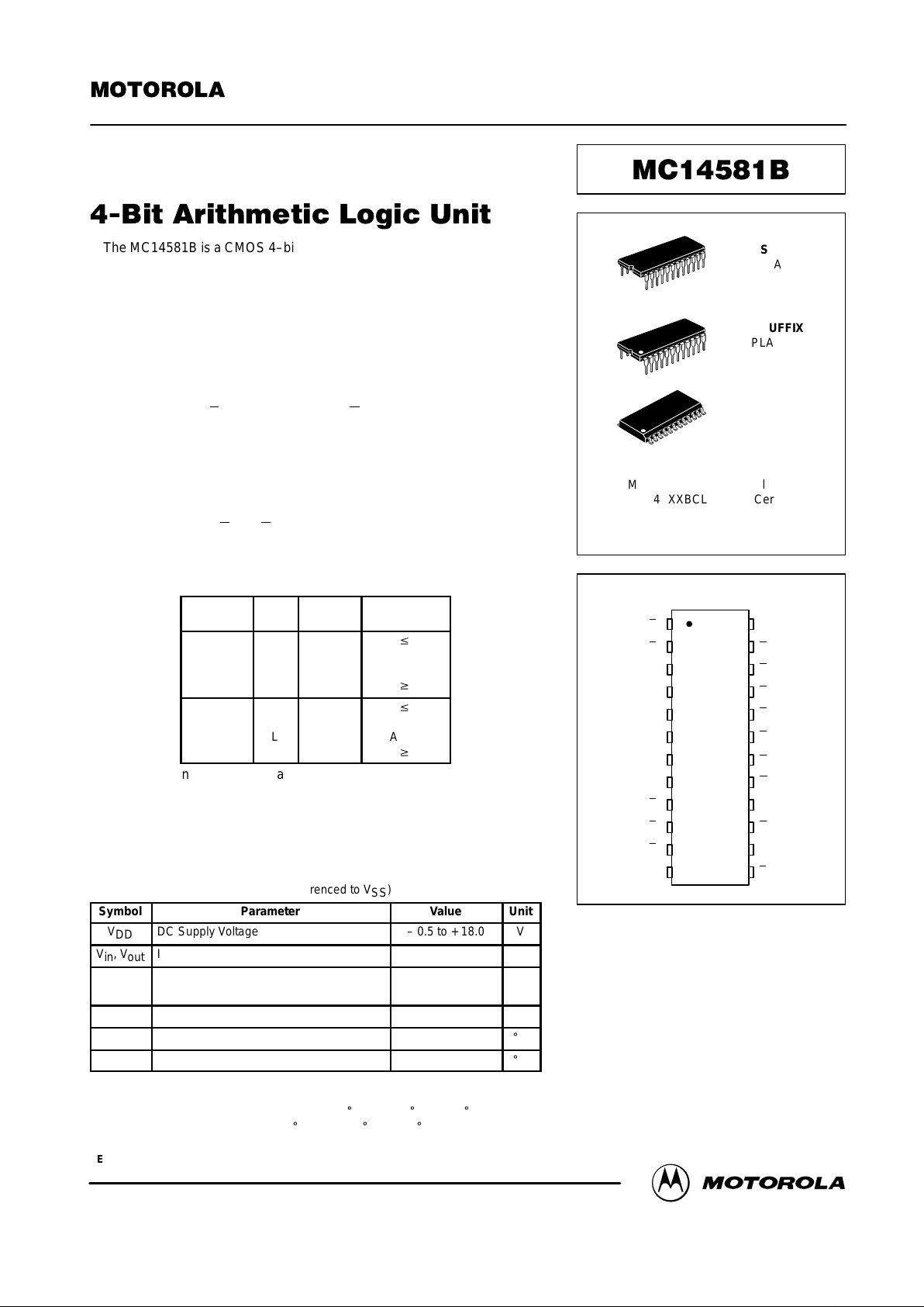
SEMICONDUCTOR TECHNICAL DATA
Motorola, Inc. 1995
REV 3
1/94
L SUFFIX
CERAMIC
CASE 623
ORDERING INFORMATION
MC14XXXBCP Plastic
MC14XXXBCL Ceramic
MC14XXXBDW SOIC
TA = – 55° to 125°C for all packages.
P SUFFIX
PLASTIC
CASE 709
DW SUFFIX
SOIC
CASE 751E
PIN ASSIGNMENT
S0
S2
S3
A
0
B
0
MC
C
n
S1 B
2
A
2
B
1
A
1
V
DD
P
C
n+4
G
5
4
3
2
1
10
9
8
7
6
14
15
16
17
18
19
20
13
11
12
21
22
23
24
F
3
A = B
B
3
A
3
F
2
V
SS
F1
F
0
MOTOROLA CMOS LOGIC DATAMC14581B
2
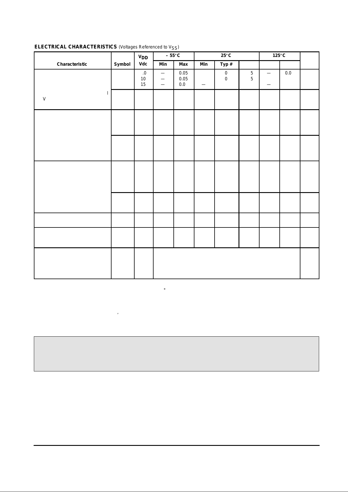
ELECTRICAL CHARACTERISTICS (Voltages Referenced to V
SS
)
V
DD
– 55_C 25_C 125_C
Characteristic
Symbol
DD
Vdc
Min Max Min Typ # Max Min Max
Unit
Output Voltage “0” Level
Vin = VDD or 0
V
OL
5.0
10
15
—
—
—
0.05
0.05
0.05
—
—
—
0
0
0
0.05
0.05
0.05
—
—
—
0.05
0.05
0.05
Vdc
“1” Level
Vin = 0 or V
DD
V
OH
5.0
10
15
4.95
9.95
14.95
—
—
—
4.95
9.95
14.95
5.0
10
15
—
—
—
4.95
9.95
14.95
—
—
—
Vdc
Input Voltage “0” Level
(VO = 4.5 or 0.5 Vdc)
(VO = 9.0 or 1.0 Vdc)
(VO = 13.5 or 1.5 Vdc)
V
IL
5.0
10
15
—
—
—
1.5
3.0
4.0
—
—
—
2.25
4.50
6.75
1.5
3.0
4.0
—
—
—
1.5
3.0
4.0
Vdc
“1” Level
(VO = 0.5 or 4.5 Vdc)
(VO = 1.0 or 9.0 Vdc)
(VO = 1.5 or 13.5 Vdc)
V
IH
5.0
10
15
3.5
7.0
11
—
—
—
3.5
7.0
11
2.75
5.50
8.25
—
—
—
3.5
7.0
11
—
—
—
Vdc
Output Drive Current
(VOH = 2.5 Vdc) Source
(VOH = 4.6 Vdc)
(VOH = 9.5 Vdc)
(VOH = 13.5 Vdc)
I
OH
5.0
5.0
10
15
– 1.2
– 0.64
– 1.6
– 4.2
—
—
—
—
– 1.0
– 0.51
– 1.3
– 3.4
– 1.7
– 0.88
– 2.25
– 8.8
—
—
—
—
– 0.7
– 0.36
– 0.9
– 2.4
—
—
—
—
mAdc
(VOL = 0.4 Vdc) Sink
(VOL = 0.5 Vdc)
(VOL = 1.5 Vdc)
I
OL
5.0
10
15
0.64
1.6
4.2
—
—
—
0.51
1.3
3.4
0.88
2.25
8.8
—
—
—
0.36
0.9
2.4
—
—
—
mAdc
Input Capacitance
(Vin = 0)
C
in
— — — — 5.0 7.5 — — pF
Quiescent Current
(Per Package)
I
DD
5.0
10
15
—
—
—
5.0
10
20
—
—
—
0.005
0.010
0.015
5.0
10
20
—
—
—
150
300
600
µAdc
Total Supply Current**†
(Dynamic plus Quiescent,
Per Package)
(CL = 50 pF on all outputs, all
buffers switching)
I
T
5.0
10
15
IT = (1.8 µA/kHz) f + I
DD
IT = (3.7 µA/kHz) f + I
DD
IT = (5.5 µA/kHz) f + I
DD
µAdc
#Data labelled “Typ” is not to be used for design purposes but is intended as an indication of the IC’s potential performance.
**The formulas given are for the typical characteristics only at 25_C.
†To calculate total supply current at loads other than 50 pF:
IT(CL) = IT(50 pF) + (CL – 50) Vfk
where: IT is in µA (per package), CL in pF, V = (VDD – VSS) in volts, f in kHz is input frequency, and k = 0.008.
This device contains protection circuitry to guard against damage due to high static voltages or electric fields. However,
precautions must be taken to avoid applications of any voltage higher than maximum rated voltages to this high-impedance
circuit. For proper operation, Vin and V
out
should be constrained to the range VSS ≤ (Vin or V
out
) ≤ VDD.
Unused inputs must always be tied to an appropriate logic voltage level (e.g., either VSS or VDD). Unused outputs must
be left open.
MOTOROLA CMOS LOGIC DATA
3
MC14581B
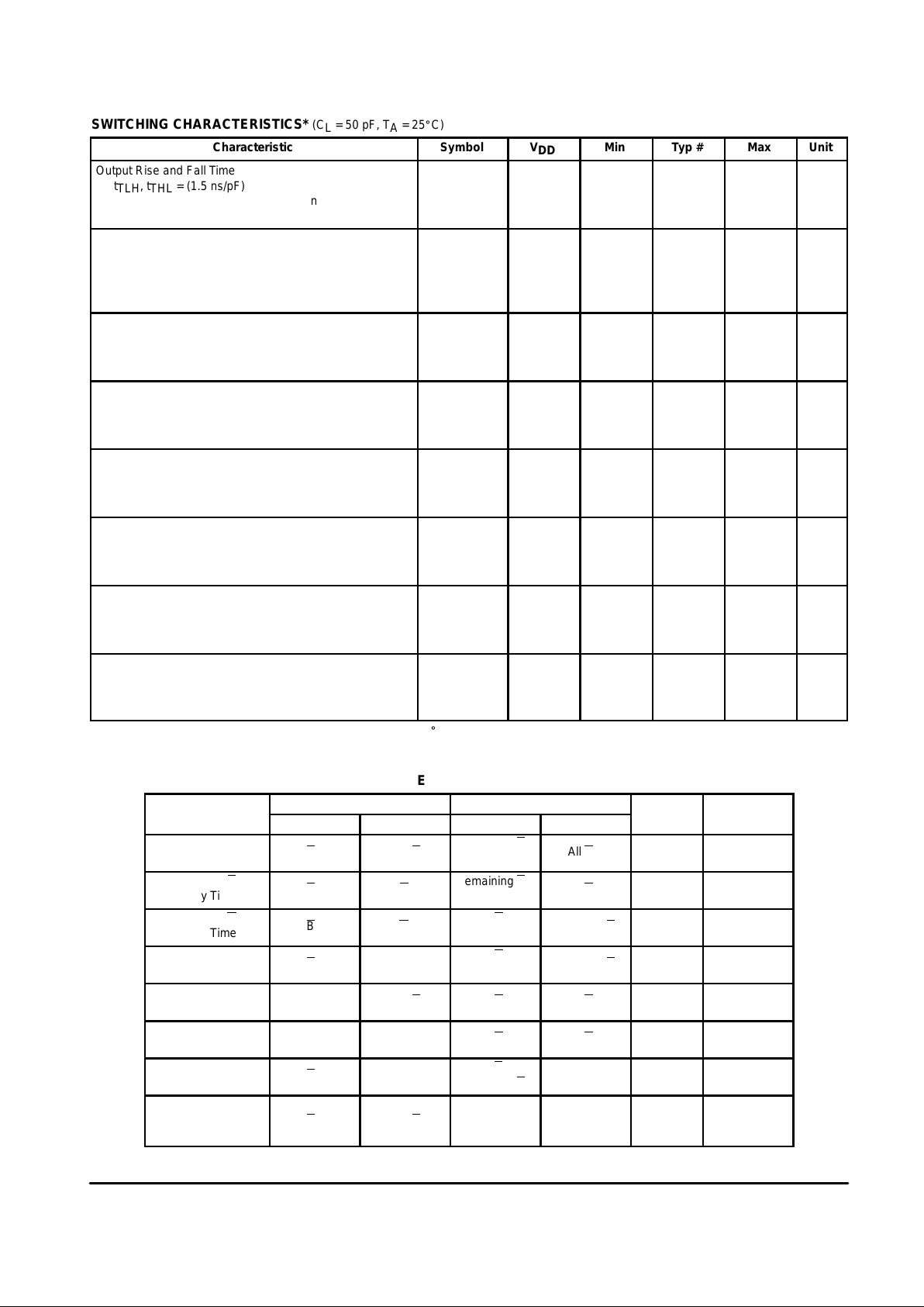
SWITCHING CHARACTERISTICS* (C
L
= 50 pF, TA = 25_C)
Characteristic
Symbol V
DD
Min Typ # Max Unit
Output Rise and Fall Time
t
TLH
, t
THL
= (1.5 ns/pF) CL + 25 ns
t
TLH
, t
THL
= (0.75 ns/pF) CL + 12.5 ns
t
TLH
, t
THL
= (0.55 ns/pF) CL + 9.5 ns
t
TLH
,
t
THL
5.0
10
15
—
—
—
100
50
40
200
100
80
ns
Propagation Delay Time
Sum in to Sum Out
t
PLH
, t
PHL
= (1.7 ns/pF) CL + 620 ns
t
PLH
, t
PHL
= (0.66 ns/pF) CL + 217 ns
t
PLH
, t
PHL
= (0.5 ns/pF) CL + 155 ns
t
PLH
,
t
PHL
5.0
10
15
—
—
—
705
250
180
1410
500
360
ns
Sum in to Sum Out (Logic Mode)
t
PLH
, t
PHL
= (1.7 ns/pF) CL + 520 ns
t
PLH
, t
PHL
= (0.66 ns/pF) CL + 182 ns
t
PLH
, t
PHL
= (0.5 ns/pF) CL + 155 ns
t
PLH
,
t
PHL
5.0
10
15
—
—
—
605
215
180
1210
430
360
ns
Sum in to A = B
t
PLH
, t
PHL
= (1.7 ns/pF) CL + 870 ns
t
PLH
, t
PHL
= (0.66 ns/pF) CL + 297 ns
t
PLH
, t
PHL
= (0.5 ns/pF) CL + 220 ns
t
PLH
,
t
PHL
5.0
10
15
—
—
—
955
330
245
1910
660
490
ns
Sum in to P or G
t
PLH
, t
PHL
= (1.7 ns/pF) CL + 400 ns
t
PLH
, t
PHL
= (0.66 ns/pF) CL + 147 ns
t
PLH
, t
PHL
= (0.5 ns/pF) CL + 105 ns
t
PLH
,
t
PHL
5.0
10
15
—
—
—
485
180
130
970
360
260
ns
Sum in to C
n+4
t
PLH
, t
PHL
= (1.7 ns/pF) CL + 530 ns
t
PLH
, t
PHL
= (0.66 ns/pF) CL + 187 ns
t
PLH
, t
PHL
= (0.5 ns/pF) CL + 135 ns
t
PLH
5.0
10
15
—
—
—
615
220
160
1230
440
360
ns
Carry in to Sum Out
t
PLH
, t
PHL
= (1.7 ns/pF) CL + 295 ns
t
PLH
, t
PHL
= (0.66 ns/pF) CL + 112 ns
t
PLH
, t
PHL
= (0.5 ns/pF) CL + 80 ns
t
PLH
,
t
PHL
5.0
10
15
—
—
—
380
145
105
760
290
210
ns
Carry in to C
n+4
t
PLH
, t
PHL
= (1.7 ns/pF) CL + 220 ns
t
PLH
, t
PHL
= (0.66 ns/pF) CL + 87 ns
t
PLH
, t
PHL
= (0.5 ns/pF) CL + 60 ns
t
PLH
,
t
PHL
5.0
10
15
—
—
—
305
120
85
610
240
170
ns
*The formulas given are for the typical characteristics only at 25_C.
#Data labelled “Typ” is not to be used for design purposes but is intended as an indication of the IC’s potential performance.
AC TEST SETUP REFERENCE TABLE
AC Paths DC Data Inputs
Fig. 3
Test
Inputs Outputs To V
SS
To V
DD
Mode
Fig. 3
Waveform
Sumin to Sum
out
Delay Time
A0 Any F
Remaining A’s
C
n
All B’s Add #1
Sumin to P
Delay Time
A0 P
Remaining A’s
C
n
All B’s Add #1
Sumin to G
Delay Time
B0 G
All A’s
C
n
Remaining B’s Add #1
Sumin to C
n+4
Delay Time
B0 C
n+y
All A’s
C
n
Remaining B’s Add #2
Cn to Sum
out
Delay Time
C
n
Any F All A’s All B’s Add #1
Cn to C
n+4
Delay Time
C
n
C
n+4
All A’s All B’s Add #1
Sumin to A = B
Delay Time
A0 A = B
All B’s
Remaining A
’s
C
n
Sub #2
Sumin to Sum
out
Delay Time
(Logic Mode)
B
0
Any F All A’s M
Exclusive
OR
#2
 Loading...